

Page 1
FEATURES
Final Electrical Specifications
LT1910
Protected High Side
MOSFET Driver
August 2002
U
DESCRIPTION
■
8V to 48V Power Supply Range
■
Protected from –15V to 60V Supply Transients
■
Short-Circuit Protected
■
Automatic Restart Timer
■
Open-Collector Fault Flag
■
Fully Enhances N-Channel MOSFET Switches
■
Programmable Current Limit, Delay Time and
Autorestart Period
■
Voltage Limited Gate Drive
■
Defaults to OFF State with Open Input
■
Available in SO-8 Package
U
APPLICATIO S
■
Industrial Control
■
Avionics Systems
■
Automotive Switches
■
Stepper Motor and DC Motor Control
■
Electronic Circuit Breaker
The LT®1910 is a high side gate driver allowing the use of
low cost N-channel power MOSFETs for high side switching applications. It contains a completely self-contained
charge pump to fully enhance an N-channel MOSFET
switch with no external components.
When the internal drain comparator senses that the switch
current has exceeded the preset level, the switch is turned
off and a fault flag is asserted. The switch remains off for
a period of time set by an external timing capacitor and
then automatically attempts to restart. If the fault still
exists, this cycle repeats until the fault is removed, thus
protecting the MOSFET. The fault flag becomes inactive
once the switch restarts successfully.
The LT1910 has been specifically designed for harsh
operating environments such as industrial, avionics and
automotive applications where poor supply regulation
and/or transients may be present. The device will not
sustain damage from supply transients of –15V to 60V.
The LT1910 is available in the SO-8 package.
, LTC and LT are registered trademarks of Linear Technology Corporation.
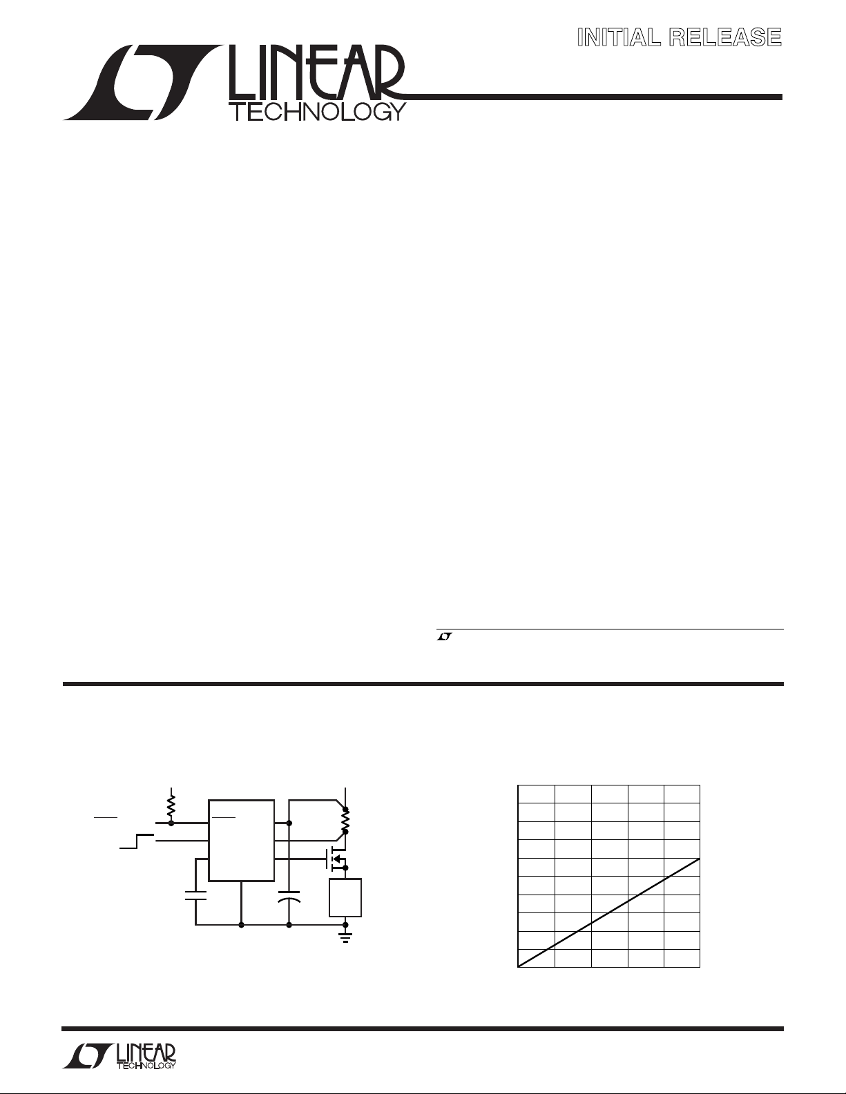
TYPICAL APPLICATIO
Fault Protected High Side Switch
5.1k
FAULT OUTPUT
OFF ON
U
Switch Drop vs Load Current
24V5V
LT1910
+
FAULT
IN
TIMER
0.1µF
V
SENSE
GATE
GND
+
10µF
50V
Information furnished by Linear Technology Corporation is believed to be accurate and reliable.
However, no responsibility is assumed for its use. Linear Technology Corporation makes no representation that the interconnection of its circuits as described herein will not infringe on existing patent rights.
0.01Ω
IRFZ34
LOAD
1910 TA01
0.50
0.45
0.40
0.35
0.30
0.25
0.20
TOTAL DROP (V)
0.15
0.10
0.05
0
0
1
3
2
LOAD CURRENT (A)
4
5
1910 TA02
1910i
1
Page 2
LT1910
WW
W
ABSOLUTE MAXIMUM RATINGS
U
U
W
PACKAGE/ORDER INFORMATION
U
(Note 1)
Supply Voltage (Pin 8)............................... –15V to 60V
Input Voltage (Pin 4) .................... (GND – 0.3V) to 15V
GATE Voltage (Pin 5) .............................................. 75V
SENSE Voltage (Pin 6)....................................... V+ ±5V
FAULT Voltage (Pin 3) ............................................ 36V
Current (Pins 1, 2, 4, 5, 6, 8) ............................... 40mA
Operating Temperature Range (Note 2) ...–40°C to 85°C
Junction Temperature Range................ –40°C to 125°C
Storage Temperature Range ................. –65°C to 150°C
GND
TIMER
FAULT
IN
T
JMAX
TOP VIEW
1
2
3
4
S8 PACKAGE
8-LEAD PLASTIC SO
= 125°C, θJA = 150°C/W
+
8
V
NC
7
SENSE
6
GATE
5
ORDER PART
NUMBER
LT1910ES8
S8 PART MARKING
1910
Lead Temperature (Soldering, 10 sec).................. 300°C
Consult LTC Marketing for parts specified with wider operating temperature ranges.
ELECTRICAL CHARACTERISTICS
range, otherwise specifications are at TA = 25°C. V+ = 12V to 48V unless otherwise noted.
SYMBOL PARAMETER CONDITIONS MIN TYP MAX UNITS
I
S
∆I
S(ON)
V
INH
V
INL
I
IN
C
IN
V
T(TH)
V
T(CL)
I
T
V
SENSE
I
SENSE
V
– V+Gate Voltage Above Supply V+ = 8V 4 4.5 6 V
GATE
V
F(TH)
V
FOL
t
ON
t
OFF
t
OFF(CL)
Supply Current (OFF State) V+ = 48V, VIN = 0.8V 1.2 1.9 2.5 mA
Delta Supply Current (ON State) VIN = 2V, Measure Increase in I
Input High Voltage ● 2V
Input Low Voltage ● 0.8 V
Input Current VIN = 2V ● 15 30 50 µA
Input Capacitance (Note 3) 5pF
Timer Threshold Voltage VIN = 2V, Adjust V
Timer Clamp Voltage VIN = 0.8V 3.2 3.5 3.8 V
Timer Charge Current VIN = VT = 2V 9 14 20 µA
Drain Sense Threshold Voltage 50 65 80 mV
Temperature Coefficient (Note 3) 0.33 %/°C
Drain Sense Input Current V+ = 48V, V
FAULT Output High Threshold Voltage VIN = 2V, IF = 1mA, Adjust V
FAULT Output Low Threshold Voltage 3.0 3.3 3.6 V
FAULT Output Low Voltage IF = 1mA ● 0.07 0.4 V
Turn-On Time V+ = 24V, V
Turn-Off Time V+ = 24V, V
Current Limit Turn-Off Time V+ = 24V, (V+ – V
The ● denotes specifications that apply over the full operating temperature
S
= 5V ● 55 110 185 µA
V
IN
T
= 65mV 0.5 1.5 µA
SENSE
+
= 12V ● 7 8.5 10 V
V
+
= 24V ● 10 12 14 V
V
V+ = 48V ● 10 12 14 V
T
GATE
GATE
= 32V, C
= 2V, C
SENSE
= 1nF 100 220 400 µs
GATE
= 1nF 25 100 µs
GATE
)→0.1V, C
= 1nF 20 50 µs
GATE
● 2.6 2.9 3.2 V
3.1 3.4 3.7 V
0.8 1.2 mA
Note 1: Absolute Maximum Ratings are those values beyond which the life
of a device may be impaired.
Note 2: The LT1910E is guaranteed to meet performance specifications
from 0°C to 70°C. Specifications over the –40°C to 85°C operating
temperature range are assured by design, characterization and correlation
with statistical process controls.
Note 3: Guaranteed but not tested.
2
1910i
Page 3
UW
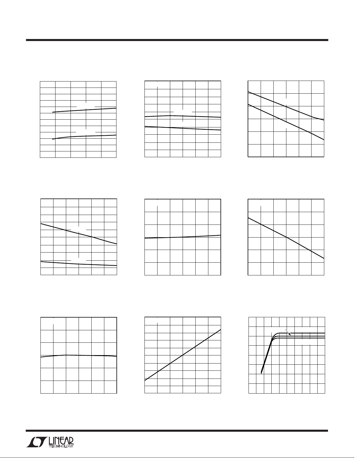
TYPICAL PERFOR A CE CHARACTERISTICS
Supply Current vs Supply Voltage Supply Current vs Temperature Input Voltage vs Temperature
3.6
3.4
3.2
3.0
2.8
2.6
2.4
2.2
2.0
SUPPLY CURRENT (mA)
1.8
1.6
1.4
1.2
10
0
SUPPLY VOLTAGE (V)
20
ON STATE
OFF STATE
30
5.0
V+ = 48V
4.5
4.0
3.5
3.0
2.5
2.0
1.5
SUPPLY CURRENT (mA)
1.0
0.5
0
–25
40
50
1910 G01
–50
ON STATE
OFF STATE
25 50
0
TEMPERATURE (°C)
75
100
1910 G02
2.0
1.8
1.6
1.4
1.2
INPUT VOLTAGE (V)
1.0
0.8
–50
–25
V
V
02550
TEMPERATURE (°C)
LT1910
INH
INL
75 100
1910 G03
Input Current vs Temperature
200
180
160
140
120
100
80
60
INPUT CURRENT (µA)
40
20
0
–50
–25
VIN = 5V
VIN = 2V
25 50
0
TEMPERATURE (°C)
Timer Charge Current
vs Temperature
20
VIN = VT = 2V
18
16
14
12
TIMER CHARGE CURRENT (µA)
10
8
–50
02550
–25
TEMPERATURE (°C)
75
100
1910 G04
75 100
1910 G07
Timer Threshold Voltage
vs Temperature
3.2
VIN = 2V
3.1
3.0
2.9
2.8
2.7
TIMER THRESHOLD VOLTAGE (V)
2.6
–50
02550
–25
TEMPERATURE (°C)
Drain Sense Threshold Voltage
vs Temperature
90
V+ = 24V
85
80
75
70
65
60
55
50
45
DRAIN SENSE THRESHOLD VOLTAGE (mV)
40
–50
–25
25 50
0
TEMPERATURE (°C)
75 100
1910 G05
75
100
1910 G08
Timer Clamp Voltage
vs Temperature
3.8
VIN ≤ 0.8V
3.7
3.6
3.5
3.4
TIMER CLAMP VOLTAGE (V)
3.3
3.2
–50
02550
–25
TEMPERATURE (°C)
MOSFET Gate Voltage Above V
(V
– V+) vs Supply Voltage
GATE
16
) (V)
+
14
– V
GATE
12
(V
+
10
8
6
4
2
0
MOSFET GATE VOLTAGE ABOVE V
0
TA = 25°C
10 20 30 503551525 45
SUPPLY VOLTAGE (V)
75 100
1910 G06
+
TA = 85°C
TA = –40°C
40
LTC1266 • F04
1910i
3
Page 4
LT1910
UW
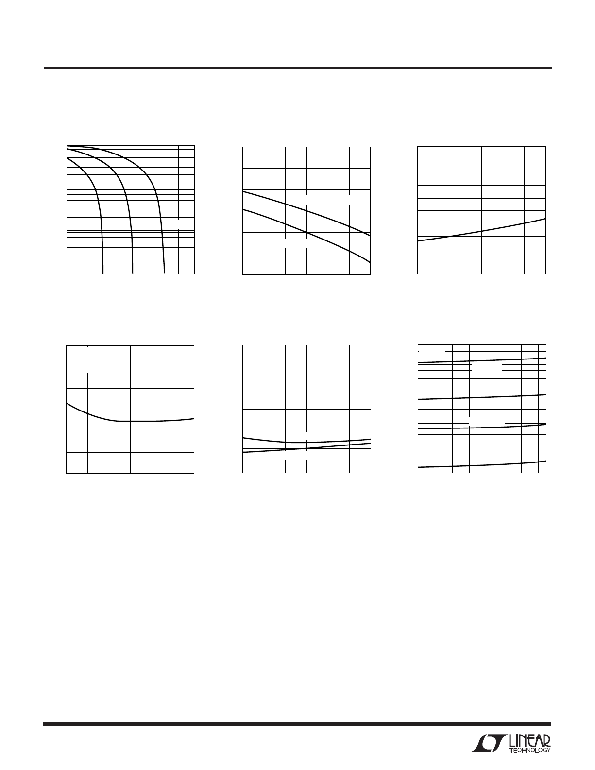
TYPICAL PERFOR A CE CHARACTERISTICS
MOSFET Gate Drive Current
vs V
100
MOSFET GATE DRIVE CURRENT (µA)
GATE
10
1
0.1
024
+
– V
V+ = 8V V+ = 12V V+ ≥ 24V
6 8 10 12 14 16
V
– V+ (V)
GATE
1910 G10
Fault Threshold Voltage
vs Temperature
3.7
VIN = 2V
= 1mA
I
F
3.6
3.5
FAULT HIGH THRESHOLD
3.4
3.3
FAULT LOW THRESHOLD
3.2
FAULT THRESHOLD VOLTAGE (V)
3.1
–50
02550
–25
TEMPERATURE (°C)
Turn-On Time vs Temperature Turn-Off Time vs Temperature
400
V+ = 24V
= 32V
V
GATE
350
300
250
200
TURN-ON TIME (µs)
150
100
–50
C
GATE
= 1nF
02550
–25
TEMPERATURE (°C)
75 100
1910 G13
100
V+ = 24V
90
80
70
60
50
40
30
TURN-OFF TIME (µs)
20
10
0
–50
V
C
GATE
GATE
= 2V
= 1nF
CURRENT LIMIT
–25
0
TEMPERATURE (°C)
NORMAL
25 50
75 100
1910 G11
75
100
1910 G014
Fault Output Low Voltage
vs Temperature
0.20
IF = 1mA
0.18
0.16
0.14
0.12
0.10
0.08
0.06
0.04
FAULT OUTPUT LOW VOLTAGE (V)
0.02
0
–50
–25
25 50
0
TEMPERATURE (°C)
Automatic Restart Period
vs Temperature
1000
V+ = 24V
CT = 3.3µF
CT = 1µF
100
CT = 0.33µF
AUTOMATIC RESTART PERIOD (ms)
10
–50
–30
CT = 0.1µF
–10 10 30 50
TEMPERATURE (°C)
75
100
1910 G012
90
70
1910 G15
4
1910i
Page 5

LT1910
U
UU
PI FU CTIO S
GND (Pin 1): Common ground.
TIMER (Pin 2): A timing capacitor CT from the TIMER pin
to ground sets the restart time following overcurrent
detection. Upon detection of an overcurrent condition, C
is rapidly discharged to less than 1V and then recharged
by a 14µA nominal current source back to the 2.9V timer
threshold, whereupon the restart is attempted. Whenever
TIMER pulls below 2.9V, the GATE pin pulls low to turn off
the external switch. This cycle repeats until the overcurrent condition goes away and the switch restarts successfully. During normal operation the pin clamps at 3.5V
nominal.
FAULT (Pin 3): The FAULT pin monitors the TIMER pin
voltage and indicates the overcurrent condition. Whenever the TIMER pin is pulled below 3.3V at the onset of a
current limit condition, the FAULT pin pulls active LOW.
The FAULT pin resets HIGH immediately when the TIMER
pin ramps above 3.4V during autorestart. The FAULT pin
is an open-collector output, thus requiring an external
pull-up resistor. This pin is intended for logic interface
with a pull-up resistor. This resistor should be selected
with a typical 1mA pull-up at low status and less than 2mA
under worst-case conditions.
T
GATE (Pin 5): The GATE pin drives the power MOSFET
gate. When the IN pin is greater than 2V, the GATE pin is
pumped approximately 12V above the supply. It has
relatively high impedance (the equivalence of a few hundred kΩ) when pumped above the rail. Care should be
taken to minimize any loading by parasitic resistance to
ground or supply. The GATE pin pulls LOW when the
TIMER pin falls below 2.9V.
SENSE (Pin 6): The SENSE pin connects to the input of a
supply-referenced comparator with a 65mV nominal offset. When the SENSE pin is taken more than 65mV below
supply, the MOSFET gate is driven LOW and the timing
capacitor is discharged. The SENSE pin threshold has a
0.33%/°C temperature coefficient (TC), which closely
matches the TC of the drain sense resistor formed from the
copper trace of the PCB.
For loads requiring high inrush current, an RC timing delay
can be added between the drain sense resistor and the
SENSE pin to ensure that the current-sense comparator
does not false trigger during start-up (see Applications
Information). A maximum of 10kΩ can be inserted between a drain sense resistor and the SENSE pin. If current
sensing is not required, the SENSE pin is tied to supply.
IN (Pin 4): The IN pin threshold is TTL/CMOS compatible
and has approximately 200mV of hysteresis. When the IN
pin is pulled active HIGH above 2V, an internal charge
pump is activated to pull up the GATE pin. The IN pin can
be pulled as high as 15V regardless of whether the supply
is on or off. If the IN pin is left open, an internal 75k pulldown resistor pulls the pin below 0.8V to ensure that the
GATE pin is inactive LOW.
V+ (Pin 8): In addition to providing the operating current
for the LT1910, the V+ pin also serves as the Kelvin
connection for the current sense comparator. The V+ pin
must be connected to the positive side of the drain sense
resistor for proper current sensing operation.
1910i
5
Page 6

LT1910
BLOCK DIAGRA
+
V
W
TIMER
IN
OPERATIO
14µA
3.3V
2.9V
1.4V
75k
75k
–
+
+
–
+
–
U
(Refer to the Block Diagram)
FAULT
+
V
+
65mV
–
+
SENSE
–
+
1.4V
–
OSCILLATOR
AND
CHARGE PUMP
GATE
250Ω
1910 BD
The LT1910 GATE pin has two states, OFF and ON. In the
OFF state it is held LOW, while in the ON state it is pumped
to 12V above the supply by a self-contained 750kHz
charge pump. The OFF state is activated when either the IN
pin is below 0.8V or the TIMER pin is below 2.9V. Conversely, for the ON state to be activated, the IN pin must be
above 2V and the TIMER pin must be above 2.9V.
The IN pin has approximately 200mV of hysteresis. If it is
left open, the IN pin is held LOW by a 75k resistor. Under
normal conditions, the TIMER pin is held a diode drop
above 2.9V by a 14µA pull-up current source. Thus the
TIMER pin automatically reverts the GATE pin to the ON
state if the IN pin is above 2V.
The SENSE pin normally connects to the drain of the power
MOSFET, which returns through a low value drain sense
resistor to supply. In order for the sense comparator to
accurately sense the MOSFET drain current, the V+ pin
must be connected directly to the positive side of the drain
sense resistor. When the GATE pin is ON and the MOSFET
drain current exceeds the level required to generate a
65mV drop across the drain sense resistor, the sense
comparator activates a pull-down NPN which rapidly pulls
the TIMER pin below 2.9V. This in turn causes the timer
comparator to override the IN pin and set the GATE pin to
the OFF state, thus protecting the power MOSFET. When
the TIMER pin is pulled below 3.3V, the fault comparator
also activates the open-collector NPN to pull the FAULT
pin LOW, indicating an overcurrent condition.
When the MOSFET gate voltage is discharged to less than
1.4V, the TIMER pin is released. The 14µA current source
then slowly charges the timing capacitor back to 2.9V
where the charge pump again starts to drive the GATE pin
HIGH. If a fault condition still exists, the sense comparator
threshold will again be exceeded and the timer cycle will
repeat until the fault is removed. The FAULT pin becomes
inactive HIGH if the TIMER pin charges up successfully
above 3.4V (see Figure 1).
1910i
6
Page 7

OPERATIO
U
GATE
LT1910
OVERCURRENTNORMAL NORMALOFF
IN
0V
12V
+
V
0V
3.5V
2.9V
TIMER
0V
5V
FAULT
0V
Figure 1. Timing Diagram
WUUU
APPLICATIO S I FOR ATIO
Input/Supply Sequencing
There are no input/supply sequencing requirements for
the LT1910. The IN pin may be taken up to 15V with the
supply at 0V. When the supply is turned on with the IN pin
set HIGH, the MOSFET turn-on will be inhibited until the
timing capacitor charges up to 2.9V (i.e., for one restart
cycle).
Isolating the Inputs
Operation in harsh environments may require isolation to
prevent ground transients from damaging control logic.
The LT1910 easily interfaces to low cost optoisolators.
The network shown in Figure 2 ensures that the input will
be pulled above 2V, but not exceed the absolute maximum
rating for supply voltages of 12V to 48V over the entire
12V TO 48V
LOGIC
INPUT
2k
LOGIC GROUND
100k
51k
LT1910
4
IN
GND
1910 F02
1
3.4V
1910 F01
temperature range. The optoisolator must have less than
20µA of dark current (leakage) at hot in order to maintain
the OFF State (see Figure 2).
Drain Sense Configuration
The LT1910 uses supply referenced current sensing. One
input of the current sense comparator is connected to a
drain sense pin, while the second input is offset 65mV below
the supply inside the device. For this reason, Pin 8 of the
LT1910 must be treated not only as a supply pin, but also
as the reference input for the current sense comparator.
Figure 3 shows the proper drain sense configuration for
the LT1910. Note that the SENSE pin goes to the drain end
of the sense resistor, while the V+ pin is connected to the
24V
5V
FAULT OUTPUT
INPUT
R1
5.1k
3
4
2
FAULT
IN
TIMER
C
T
1µF
LT1910
SENSE
GND
1
GATE
8
+
V
6
5
+
C1
100µF
50V
R
S
0.02Ω
(PTC)
Q1
IRFZ34
24V
2A
SOLENOID
POWER GROUND
Figure 2. Isolating the Input
0V
Figure 3. Drain Sense Configuration
1910 F03
1910i
7
Page 8

LT1910
WUUU
APPLICATIO S I FOR ATIO
supply at the same point as the positive end of the sense
resistor.
The drain sense threshold voltage has a positive temperature coefficient, allowing PTC sense resistors to be used
(see Printed Circuit Board Shunts). The selection of R
S
should be based on the minimum threshold voltage:
RS = 50mV/I
SET
Thus the 0.02Ω drain sense resistor in Figure 3 will yield
a minimum trip current of 2.5A. This simple configuration
is appropriate for resistive or inductive loads that do not
generate large current transients at turn-on.
Automatic Restart Period
The timing capacitor CT shown in Figure 3 determines the
length of time the power MOSFET is held off following a
current limit trip. Curves are given in the Typical Performance Characteristics to show the restart period for
various values of CT. For example, CT = 0.33µF yields a
50ms restart period.
Defeating Automatic Restart
Some applications are required to remain off after a fault
occurs. When the LT1910 is being driven from CMOS
logic, this can be easily implemented by connecting resistor R2 between the IN and TIMER pins as shown in
Figure␣ 4. R2 supplies the sustaining current for an internal
SCR which latches the TIMER pin LOW under a fault
condition. The FAULT pin is set active LOW when the
TIMER pin falls below 3.3V. This keeps the MOSFET gate
from turning ON and the FAULT pin from resetting HIGH
5V
R1
5.1k
3
FAULT
4
IN
LT1910
2
CT
1µF
TIMER
GND
1
1910 F04
R2
2k
5V
CMOS
LOGIC
FAULT OUTPUT
ON = 5V
OFF = 0V
until the IN pin has been recycled. CT is used to prevent the
FAULT pin from glitching whenever the IN pin recycles to
turn on the MOSFET unsuccessfully under an existing fault
condition.
Inductive vs Capacitive Loads
Turning on an inductive load produces a relatively benign
ramp in MOSFET current. However, when an inductive
load is turned off, the current stored in the inductor needs
somewhere to decay. A clamp diode connected directly
across each inductive load normally serves this purpose.
If a diode is not employed, the LT1910 clamps the MOSFET
gate 0.7V below ground. This causes the MOSFET to
resume conduction during the current decay with (V+ +
VGS + 0.7V) across it, resulting in high dissipation peaks.
Capacitive loads exhibit the opposite behavior. Any load
that includes a decoupling capacitor will generate a current equal to C
• (∂V/∂t) during capacitor in-rush.
LOAD
With large electrolytic capacitors, the resulting current
spike can play havoc with the power supply and false trip
the current sense comparator.
Turn-on ∂V/∂t is controlled by the addition of the simple
network shown in Figure 5. This network takes advantage
of the fact that the MOSFET acts as a source follower
during turn-on. Thus the ∂V/∂t on the source can be
controlled by controlling the ∂V/∂t on the gate.
SENSE
LT1910
GND
1
GATE
50µF
V
50V
8
+
6
∂V/∂t CONTROL NETWORK
5
+
C2
CURRENT LIMIT
DELAY NETWORK
1N4148
C
D
RD (≤10k)
1N4148
R1
100kR2100k
C1
+
24V
R
S
0.01Ω
Q1
IRFZ34
15V
1N4744
C
LOAD
1910 F05
Figure 4. Latch-Off Configuration (Autorestart Defeated)
8
Figure 5. Control and Current Limit Delay
1910i
Page 9

WUUU
APPLICATIO S I FOR ATIO
LT1910
The turn-on current spike into C
VV
–
IC
= •
PEAK LOAD
GTH
RC
•11
is estimated by:
LOAD
where VTH is the MOSFET gate threshold voltage. VG is
obtained by plotting the equation:
V
I
GATE
on the graph of Gate Drive Current (I
(V
GATE
GATE
=
R
1
) vs Gate Voltage
GATE
) as shown in Figure 6. The value of V
GATE
at the
intersection of the curves for a given supply is VG. For
example, if V+ = 24V and R1 = 100k, then VG = 18.3V. For
VTH = 2V, C1 = 0.1µF and C
I
= 1.6A. The diode and the second resistor in the
PEAK
= 1000µF, the estimated
LOAD
network ensure fast current limit turn-off.
When turning off a capacitive load, the source of the
MOSFET can “hang up” if the load resistance does not
discharge C
as fast as the gate is being pulled down.
LOAD
If this is the case, a 15V zener may be added from gate to
source to prevent V
800
700
600
V+ = 24V
500
400
300
200
GATE DRIVE CURRENT (µA)
100
0
10 20 40
0
Figure 6. Gate Drive Current vs Gate Voltage
GS(MAX)
V+ = 12V
V+ = 8V
from being exceeded.
V+ = 48V
I
GATE
V
GATE
30
GATE VOLTAGE (V)
50
=
/10
1910 F06
5
60
Adding Current Limit Delay
When capacitive loads are being switched or in very noisy
environments, it is desirable to add delay in the drain
current sense path to prevent false tripping (inductive
loads normally do not need delay). This is accomplished
by the current limit delay network shown in Figure 5. R
D
and CD delay the overcurrent trip for drain currents up to
approximately 10 • I
, above which the diode conducts
SET
and provides immediate turn-off (see Figure 7). To ensure
proper operation of the timer, CD must be ≤CT.
10
)
D
C
D
1
0.1
TRIP DELAY TIME (1 = R
0.01
1
MOSFET DRAIN CURRENT (1 = SET CURRENT)
Figure 7. Current Limit Delay Time
10 100
1910 F07
Printed Circuit Board Shunts
The sheet resistance of 1oz copper clad is approximately
5 • 10–4Ω/square with a temperature coefficient of
0.39%/°C. Since the LT1910 drain sense threshold has a
similar temperature coefficient (0.33%/°C), this offers the
possibility of nearly zero TC current sensing using the
“free”
drain sense resistor made out of PC trace material.
A conservative approach is to use 0.02" of width for each
1A of current for 1oz copper. Combining the LT1910 drain
sense threshold with the 1oz copper resistance results in
a simple expression for width and length:
Width (1oz Cu) = 0.02" • I
SET
Length (1oz Cu) = 2"
The width for 2oz copper would be halved while the length
would remain the same.
Bends may be incorporated into the resistor to reduce
space; each bend is equivalent to approximately 0.6 • the
width of a straight length. Kelvin connection should be
employed by running a separate trace from the ends of the
resistor back to the LT1910’s V+ and SENSE pins. See
Application Note 53 for further information on printed
circuit board shunts.
1910i
9
Page 10

LT1910
WUUU
APPLICATIO S I FOR ATIO
Low Voltage/Wide Supply Range Operation
When the supply is less than 12V, the LT1910’s charge
pump does not produce sufficient gate voltage to fully
enhance the standard N-channel MOSFET. For these applications, a logic-level MOSFET can be used to extend the
operating supply down to 8V. If the MOSFET has a maximum VGS rating of 15V or greater, then the LT1910 can
also operate up to a supply voltage of 60V (absolute
maximum rating of the V+ pin).
Protecting Against Supply Transients
The LT1910 is 100% tested and guaranteed to be safe
from damage with 60V applied between the V+ and GND
pins. However, when this voltage is exceeded, even for a
few microseconds, the result can be catastrophic. For this
reason it is imperative that the LT1910 is not exposed to
supply transients above 60V. A transient suppressor, such
as Diodes Inc.’s SMAJ48A, should be added between the
V+ and GND pins for such applications.
For proper current sense operation, the V+ pin is required
to be connected to the positive side of the drain sense
resistor (see Drain Sense Configuration). Therefore, the
supply should be adequately decoupled at the node where
the V+ pin and drain sense resistor meet. Several hundred
microfarads may be required when operating with a high
current switch.
When the operating voltage approaches the 60V absolute
maximum rating of the LT1910, local supply decoupling
between the V+ and GND pins is highly recommended. An
RC snubber with a transient suppressor are an absolute
necessity. Note however that resistance should not be
added in series with the V+ pin because it will cause an
error in the current sense threshold.
Low Side Driving
Although the LT1910 is primarily targeted at high side
(grounded load) switch applications, it can also be used
for low side (supply connected load) switch applications.
Figures 8a and 8b illustrate the LT1910 driving low side
power MOSFETs. Because the LT1910 charge pump tries
to pump the gate of the N-channel MOSFET above the
supply, a clamp zener is required to prevent the V
GS
(absolute maximum) of the MOSFET from being exceeded.
12V TO 48V
5V
R1
5.1k
FAULT OUTPUT
INPUT
3
FAULTINV
4
LT1910
2
GND
C
T
1µF
0V
SENSE
GATETIMER
1
8
+
6
+
C1
100µF
100V
5
15V
1N4744
Figure 8a. Low Side Driver with Load Current Sensing
4A
LOAD
R
S
0.01Ω
(PTC)
Q1
IRFZ44
1910 F08a
10
FAULT OUTPUT
INPUT
5V
R1
5.1k
3
4
2
FAULT
IN
TIMER
C
T
1µF
LT1910
GND
8V TO 24V HV
8
+
SENSE
GATE
1
V
10µF
50V
6
5
+
C1
2N2222
51Ω
1N4744
LT1006
51Ω
Figure 8b. Low Side Driver for Source Current Sensing
15V
HV
LOAD
Q1
IRF630
+
R
S
0.02Ω
–
1910 F08b
1910i
Page 11

WUUU
APPLICATIO S I FOR ATIO
LT1910
The LT1910 gate drive is current limited for this purpose
so that no resistance is needed between the GATE pin and
zener.
Current sensing for protecting low side drivers can be
done in several ways. In the Figure 8a circuit, the supply
voltage for the load is assumed to be within the supply
operating range of the LT1910. This allows the load to be
returned to supply through current sense resistor RS,
providing normal operation of the LT1910 protection
circuitry.
U
PACKAGE DESCRIPTIO
S8 Package
8-Lead Plastic Small Outline (Narrow .150 Inch)
(Reference LTC DWG # 05-08-1610)
If the load cannot be returned to supply through RS, or the
load supply voltage is higher than the LT1910 supply, the
current sense must be moved to the source of the low side
MOSFET.
Figure 8b shows an approach to source sensing. An
operational amplifier (must common mode to ground) is
used to level shift the voltage across RS up to the drain
sense pin. This approach allows the use of a small sense
resistor which could be made from PC trace material. The
LT1910 restart timer functions the same as in the high side
switch application.
0.189 – 0.197*
(4.801 – 5.004)
7
8
5
6
0.228 – 0.244
(5.791 – 6.197)
0.010 – 0.020
(0.254 – 0.508)
0.008 – 0.010
(0.203 – 0.254)
*
DIMENSION DOES NOT INCLUDE MOLD FLASH. MOLD FLASH
SHALL NOT EXCEED 0.006" (0.152mm) PER SIDE
**
DIMENSION DOES NOT INCLUDE INTERLEAD FLASH. INTERLEAD
FLASH SHALL NOT EXCEED 0.010" (0.254mm) PER SIDE
×
°
45
0.016 – 0.050
(0.406 – 1.270)
0°– 8° TYP
0.053 – 0.069
(1.346 – 1.752)
0.014 – 0.019
(0.355 – 0.483)
TYP
0.150 – 0.157**
(3.810 – 3.988)
1
3
2
4
0.004 – 0.010
(0.101 – 0.254)
0.050
(1.270)
BSC
SO8 1298
1910i
11
Page 12

LT1910
TYPICAL APPLICATIO
Protected 1A Automotive Solenoid Driver with Overvoltage Shutdown
8V TO 24V OPERATING
32V TO 60V SHUTDOWN
POWER
GROUND
U
FAULT OUTPUT
30V
1N6011B
R2
10k
R3
5.1k
INPUT
5V
1N4148
2N3904
R1
5.1k
3
4
2
FAULT
IN
TIMER
C
T
1µF
LT1910
SENSE
GND
1
GATE
R
8
+
V
6
5
+
C1
10µF
100V
S
0.03Ω
(PTC)
Q1
MTD3055EL
24V
1A
SOLENOID
1910 TA03
RELATED PARTS
PART NUMBER DESCRIPTION COMMENTS
LTC®1153 Autoreset Electronic Circuit Breaker Programmable Trip Current, Fault Status Output
LTC1155 Dual High Side Micropower MOSFET Driver Operates from 4.5V to 18V, 85µA ON Current, Short-Circuit Protection
LT1161 Quad Protected High Side MOSFET Driver 8V to 48V Supply Range, Individual Short-Circuit Protection
LTC1163 Triple 1.8V to 6V High Side MOSFET Driver 0.01µA Standby Current, Triple Driver in SO-8 Package
LTC1255 Dual 24V High Side MOSFET Driver Operates from 9V to 24V, Short-Circuit Protection
LTC1477 Protected Monolithic High Side Switch Low R
LTC1623 SMBus Dual High Side Switch Controller 2-Wire SMBus Serial Interface, Built-In Gate Charge Pumps
LTC1693 Family High Speed Single/Dual N-Channel/P-Channel 1.5A Peak Output Current, 4.5V ≤ VCC ≤ 13.2V, SO-8 Package
MOSFET Drivers
LTC1710 SMBus Dual Monolithic High Side Switch Two Low R
LTC4412 Low Loss PowerPathTM Controller Implements “Ideal Diode” Function, ThinSOTTM Package
PowerPath and ThinSOT are trademarks of Linear Technology Corporation.
0.07Ω Switch, 2A Short-Circuit Protected
DS(ON)
0.4Ω/300mA Switches in 8-Lead MSOP Package
DS(ON)
12
Linear Technology Corporation
1630 McCarthy Blvd., Milpitas, CA 95035-7417
(408) 432-1900 ● FAX: (408) 434-0507
●
www.linear.com
1910i
LT/TP 0802 1.5K • PRINTED IN USA
LINEAR TECHNOLOGY CORPORATION 2002
 Loading...