

Page 1
FEATURES
LINE VOLTAGE (V
P-P
)
0
HARMONIC DISTORTION (dBc)
–60
–70
–80
–90
–100
1886 TA01a
2 4 6 8 10 12 14 16
VS = 12V
A
V
= 10
f = 200kHz
100Ω LINE
1:2 TRANSFORMER
HD2
HD3
■
700MHz Gain Bandwidth
■
±200mA Minimum I
■
Low Distortion: –72dBc at 1MHz, 4V
■
Stable in AV ≥ 10, Simple Compensation for AV < 10
■
±4.3V Minimum Output Swing, VS = ±6V, RL = 25Ω
■
7mA Supply Current per Amplifier
■
200V/µs Slew Rate
■
Stable with 1000pF Load
■
6nV/√Hz Input Noise Voltage
■
2pA/√Hz Input Noise Current
■
4mV Maximum Input Offset Voltage
■
4µA Maximum Input Bias Current
■
400nA Maximum Input Offset Current
■
±4.5V Minimum Input CMR, VS = ±6V
■
Specified at ±6V, ±2.5V
OUT
, 25Ω, A
P-P
U
APPLICATIO S
V
= 2
LT1886
Dual 700MHz, 200mA
Operational Amplifier
U
DESCRIPTIO
The LT®1886 is a 200mA minimum output current dual op
amp with outstanding distortion performance. The amplifiers are gain-of-ten stable, but can be easily compensated
for lower gains. The LT1886 features balanced, high
impedance inputs with 4µA maximum input bias current,
and 4mV maximum input offset voltage. Single supply
applications are easy to implement and have lower total
noise than current feedback amplifier implementations.
The output drives a 25Ω load to ±4.3V with ±6V supplies.
On ±2.5V supplies the output swings ±1.5V with a 100Ω
load. The amplifier is stable with a 1000pF capacitive
load which makes it useful in buffer and cable driver
applications.
The LT1886 is manufactured on Linear Technology’s
advanced low voltage complementary bipolar process and
is available in a thermally enhanced SO-8 package.
■
DSL Modems
■
xDSL PCI Cards
■
USB Modems
■
Line Drivers
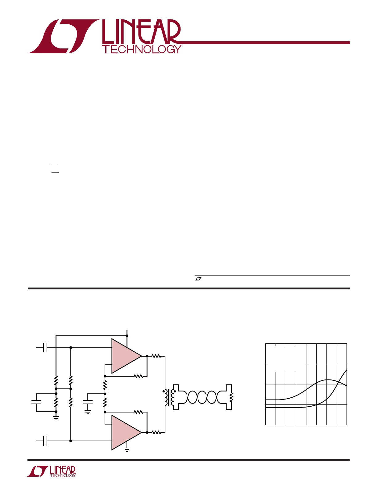
TYPICAL APPLICATIO
0.1µF
+
IN
1µF
0.1µF
–
IN
10k 20k
U
Single 12V Supply ADSL Modem Line Driver
12V
+
1/2 LT1886
–
100Ω
20k10k
1µF
100Ω
–
1/2 LT1886
+
909Ω
909Ω
12.4Ω
12.4Ω
1:2*
1886 TA01
, LTC and LT are registered trademarks of Linear Technology Corporation.
ADSL Modem Line Driver Distortion
100Ω
*COILCRAFT X8390-A
OR EQUIVALENT
1
Page 2
LT1886
1
2
3
4
8
7
6
5
TOP VIEW
V
+
OUT B
–IN B
+IN B
OUT A
–IN A
+IN A
V
–
S8 PACKAGE
8-LEAD PLASTIC SO
B
A
WW
W
ABSOLUTE MAXIMUM RATINGS
U
PACKAGE
/
O
RDER I FOR ATIO
WU
(Note 1)
Total Supply Voltage (V+ to V–) ........................... 13.2V
Input Current (Note 2) ....................................... ±10mA
Input Voltage (Note 2) ............................................ ±V
Maximum Continuous Output Current (Note 3)
S
ORDER PART
NUMBER
LT1886CS8
DC ............................................................... ±100mA
AC ............................................................... ±300mA
Operating Temperature Range (Note 10) –40°C to 85°C
Specified Temperature Range (Note 9).. – 40°C to 85°C
T
= 150°C, θJA = 80°C/W (Note 4)
JMAX
S8 PART MARKING
1886
Maximum Junction Temperature ......................... 150°C
Storage Temperature Range ................ –65°C to 150°C
Consult factory for Industrial and Military grade parts.
Lead Temperature (Soldering, 10 sec)................. 300°C
ELECTRICAL CHARACTERISTICS
erature range, otherwise specifications are at T
SYMBOL PARAMETER CONDITIONS MIN TYP MAX UNITS
V
OS
I
OS
I
B
e
n
i
n
R
IN
C
IN
CMRR Common Mode Rejection Ratio VCM = ±4.5V ● 77 98 dB
PSRR Power Supply Rejection Ratio VS = ±2V to ±6.5V 80 86 dB
A
VOL
V
OUT
I
SC
Input Offset Voltage (Note 5) 1 4 mV
Input Offset Voltage Drift (Note 8) ● 317µV/°C
Input Offset Current 150 400 nA
Input Bias Current 1.5 4 µA
Input Noise Voltage f = 10kHz 6 nV/√Hz
Input Noise Current f = 10kHz 2 pA/√Hz
Input Resistance VCM = ±4.5V 5 10 MΩ
Input Capacitance 2pF
Input Voltage Range (Positive) ● 4.5 5.9 V
Input Voltage Range (Negative)
Minimum Supply Voltage Guaranteed by PSRR ● ±2V
Large-Signal Voltage Gain V
Output Swing RL = 100Ω, 10mV Overdrive 4.85 5 ±V
Short-Circuit Current (Sourcing) (Note 3) 800 mA
Short-Circuit Current (Sinking) 500 mA
= 25°C. VS = ±6V, V
A
Differential 35 kΩ
= ±4V, RL = 100Ω 5.0 12 V/mV
OUT
V
= ±4V, RL = 25Ω 4.5 12 V/mV
OUT
RL = 25Ω, 10mV Overdrive 4.30 4.6 ±V
I
= 200mA, 10mV Overdrive 4.30 4.5 ±V
OUT
The ● denotes specifications which apply over the full operating temp-
= 0V, pulse power tested unless otherwise noted. (Note 9)
CM
● 5mV
● 600 nA
● 6 µA
● –5.2 –4.5 V
● 78 dB
● 4.5 V/mV
● 4.0 V/mV
● 4.70 ±V
● 4.10 ±V
● 4.10 ±V
2
U
Page 3
LT1886
ELECTRICAL CHARACTERISTICS
erature range, otherwise specifications are at T
= 25°C. VS = ±6V, V
A
The ● denotes specifications which apply over the full operating temp-
= 0V, pulse power tested unless otherwise noted. (Note 9)
CM
SYMBOL PARAMETER CONDITIONS MIN TYP MAX UNITS
SR Slew Rate AV = –10 (Note 6) 133 200 V/µs
● 110 V/µs
Full Power Bandwidth 4V Peak (Note 7) 8 MHz
GBW Gain Bandwidth f = 1MHz 700 MHz
tr, t
Rise Time, Fall Time AV = 10, 10% to 90% of 0.1V, RL = 100Ω 4ns
f
Overshoot AV = 10, 0.1V, RL = 100Ω 1%
Propagation Delay AV = 10, 50% VIN to 50% V
t
S
Settling Time 6V Step, 0.1% 50 ns
Harmonic Distortion HD2, AV = 10, 2V
= 10, 2V
HD3, A
V
, f = 1MHz, RL = 100Ω/25Ω – 75/–63 dBc
P-P
, f = 1MHz, RL = 100Ω/25Ω – 85/–71 dBc
P-P
, 0.1V, RL = 100Ω 2.5 ns
OUT
IMD Intermodulation Distortion AV = 10, f = 0.9MHz, 1MHz, 14dBm, RL = 100Ω/25Ω –81/–80 dBc
R
OUT
I
S
Output Resistance AV = 10, f = 1MHz 0.1 Ω
Channel Separation V
= ±4V, RL = 25Ω 82 92 dB
OUT
● 80 dB
Supply Current Per Amplifier 7 8.25 mA
● 8.50 mA
The ● denotes specifications which apply over the full operating temperature range, otherwise specifications are at TA = 25°C.
V
= ±2.5V, V
S
SYMBOL PARAMETER CONDITIONS MIN TYP MAX UNITS
V
OS
I
OS
I
B
e
n
i
n
R
IN
C
IN
CMRR Common Mode Rejection Ratio VCM = ±1V ● 75 91 dB
A
VOL
V
OUT
= 0V, pulse power tested unless otherwise noted. (Note 9)
CM
Input Offset Voltage (Note 5) 1.5 5 mV
● 6mV
Input Offset Voltage Drift (Note 8) ● 517µV/°C
Input Offset Current 100 350 nA
● 550 nA
Input Bias Current 1.2 3.5 µA
● 5.5 µA
Input Noise Voltage f = 10kHz 6 nV/√Hz
Input Noise Current f = 10kHz 2 pA/√Hz
Input Resistance VCM = ±1V 10 20 MΩ
Differential 50 kΩ
Input Capacitance 2pF
Input Voltage Range (Positive) ● 1 2.4 V
Input Voltage Range (Negative)
Large-Signal Voltage Gain V
= ±1V, RL = 100Ω 5.0 10 V/mV
OUT
V
= ±1V, RL = 25Ω 4.5 10 V/mV
OUT
● –1.7 –1 V
● 4.5 V/mV
● 4.0 V/mV
Output Swing RL = 100Ω, 10mV Overdrive 1.50 1.65 ±V
● 1.40 ±V
RL = 25Ω, 10mV Overdrive 1.35 1.50 ±V
● 1.25 ±V
I
= 200mA, 10mV Overdrive 0.87 1 ±V
OUT
● 0.80 ±V
3
Page 4
LT1886
ELECTRICAL CHARACTERISTICS
erature range, otherwise specifications are at T
= 25°C. VS = ±2.5V, V
A
The ● denotes specifications which apply over the full operating temp-
= 0V, pulse power tested unless otherwise noted. (Note 9)
CM
SYMBOL PARAMETER CONDITIONS MIN TYP MAX UNITS
I
SC
Short-Circuit Current (Sourcing) (Note 3) 600 mA
Short-Circuit Current (Sinking) 400 mA
SR Slew Rate AV = –10 (Note 6) 66 100 V/µs
● 60 V/µs
Full Power Bandwidth 1V Peak (Note 7) 16 MHz
GBW Gain Bandwidth f = 1MHz 530 MHz
tr, t
Rise Time, Fall Time AV = 10, 10% to 90% of 0.1V, RL = 100Ω 7ns
f
Overshoot AV = 10, 0.1V, RL = 100Ω 5%
Propagation Delay AV = 10, 50% VIN to 50% V
Harmonic Distortion HD2, AV = 10, 2V
= 10, 2V
HD3, A
V
, f = 1MHz, RL = 100Ω/25Ω – 75/–64 dBc
P-P
, f = 1MHz, RL = 100Ω/25Ω – 80/–66 dBc
P-P
, 0.1V, RL = 100Ω 5ns
OUT
IMD Intermodulation Distortion AV = 10, f = 0.9MHz, 1MHz, 5dBm, RL = 100Ω/25Ω – 77/–85 dBc
R
OUT
I
S
Note 1: Absolute Maximum Ratings are those values beyond which the life
of a device may be impaired.
Note 2: The inputs are protected by back-to-back diodes. If the differential
input voltage exceeds 0.7V, the input current should be limited to less than
10mA.
Note 3: A heat sink may be required to keep the junction temperature
below absolute maximum.
Note 4: Thermal resistance varies depending upon the amount of PC board
metal attached to the device. θ
covered with 2 oz copper on both sides.
Note 5: Input offset voltage is exclusive of warm-up drift.
Output Resistance AV = 10, f = 1MHz 0.2 Ω
Channel Separation V
= ±1V, RL = 25Ω 82 92 dB
OUT
● 80 dB
Supply Current Per Amplifier 5 5.75 mA
● 6.25 mA
Note 6: Slew rate is measured between ±2V on a ±4V output with ±6V
supplies, and between ±1V on a ±1.5V output with ±2.5V supplies.
Note 7: Full power bandwidth is calculated from the slew rate:
FPBW = SR/2πV
.
P
Note 8: This parameter is not 100% tested.
Note 9: The LT1886C is guaranteed to meet specified performance from 0°C
to 70°C. The LT1886C is designed, characterized and expected to meet
specified performance from –40°C to 85°C but is not tested or QA sampled
is specified for a 2500mm2 test board
JA
at these temperatures. For guaranteed I-grade parts, consult the factory.
Note 10: The LT1886C is guaranteed functional over the operating temperature
range of –40°C to 85°C.
UW
TYPICAL PERFOR A CE CHARACTERISTICS
Input Common Mode Range vs
Supply Current vs Temperature
15
VS = ±6V
10
VS = ±2.5V
5
SUPPLY CURRENT (mA)
0
–50 –25 0 25 50 75 100 125
TEMPERATURE (°C)
1886 G01
Supply Voltage
+
V
–0.1
–0.2
–0.3
TA = 25°C
> 1mV
∆V
1.5
1.0
COMMON MODE RANGE (V)
0.5
V
OS
–
0 2 4 6 8 10 12 14
TOTAL SUPPLY VOLTAGE (V)
4
1886 G02
Input Bias Current vs Input
Common Mode Voltage
3.0
TA = 25°C
= (I
+ + IB–)/2
I
B
2.5
2.0
1.5
1.0
INPUT BIAS CURRENT (µA)
0.5
0
B
VS = ±6V
VS = ±2.5V
–6 –2 2–4 0 4 6
INPUT COMMON MODE VOLTAGE (V)
1886 G03
Page 5
UW
TYPICAL PERFOR A CE CHARACTERISTICS
LT1886
Input Bias Current vs
Temperature Input Noise Spectral Density
3.5
IB = (I
+ + IB–)/2
3.0
2.5
2.0
1.5
1.0
INPUT BIAS CURRENT (µA)
0.5
0
B
VS = ±6V
VS = ±2.5V
–50 –25 0 25 50 75 100 125
TEMPERATURE (°C)
Output Saturation Voltage vs
Temperature, V
+
V
–0.5
–1.0
–1.5
1.5
1.0
0.5
OUTPUT SATURATION VOLTAGE (V)
–
V
IL = 150mA IL = 200mA
IL = 150mA IL = 200mA
–50 –25 0 25 50 75 100 125
= ±6V
S
RL = 100Ω
RL = 100Ω
TEMPERATURE (°C)
1886 G04
1886 G07
100
TA = 25°C
= 101
A
V
10
INPUT VOLTAGE NOISE (nV/√Hz)
1
10
1k 100k100 10k
FREQUENCY (Hz)
Output Saturation Voltage vs
Temperature, V
+
V
–0.5
–1.0
–1.5
1.5
1.0
0.5
OUTPUT SATURATION VOLTAGE (V)
–
V
–50 –25 0 25 50 75 100 125
IL = 150mA IL = 200mA
IL = 150mA IL = 200mA
TEMPERATURE (°C)
Output Short-Circuit Current vs
Temperature
100
10
e
n
i
n
1
1886 G05
= ±2.5V Settling Time vs Output Step
S
RL = 100Ω
RL = 100Ω
1886 G08
1000
900
INPUT CURRENT NOISE (pA/√Hz)
800
700
600
500
400
300
200
100
OUTPUT SHORT-CIRCUIT CURRENT (mA)
0
–50 –25 0 25 50 75 100 125
6
4
2
0
–2
OUTPUT STEP (V)
–4
–6
0204010 30 50 60
SOURCE, VS = ±6V
SOURCE, VS = ±2.5V
SINK, VS = ±6V
SINK, VS = ±2.5V
∆VIN = 0.2V
TEMPERATURE (°C)
VS = ±6V
SETTLING TIME (ns)
10mV 1mV
10mV 1mV
1886 G06
1886 G09
Gain and Phase vs Frequency
80
70
60
50
40
30
GAIN (dB)
20
10
0
–10
–20
1M
TA = 25°C
= –10
A
V
= 100Ω
R
L
PHASE
VS = ±2.5V
VS = ±6V
VS = ±2.5V
GAIN
10M 100M 1G
FREQUENCY (Hz)
VS = ±6V
1886 G10
100
80
60
40
PHASE (DEG)
20
0
–20
–40
–60
–80
–100
Gain Bandwidth vs Supply
Voltage Output Impedance vs Frequency
800
TA = 25°C
= –10
A
V
700
600
500
GAIN BANDWIDTH (MHz)
400
300
2 4 6 8 10 12 14
0
TOTAL SUPPLY VOLTAGE (V)
RL = 1k
RL = 100Ω
RL = 25Ω
1886 G11
100
10
1
0.1
OUTPUT IMPEDANCE (Ω)
0.01
100k 10M 100M
AV = 100
AV = 10
1M
FREQUENCY (Hz)
1886 G12
5
Page 6

LT1886
UW
TYPICAL PERFOR A CE CHARACTERISTICS
Frequency Response vs Supply
Voltage, AV = 10
23
TA = 25°C
22
= 10
A
V
21
= 100Ω
R
L
20
19
18
GAIN (dB)
17
16
15
14
13
1M 100M 1G
VS = ±2.5V
10M
FREQUENCY (Hz)
VS = ±6V
Frequency Response vs Supply
Voltage, AV = –1
3
2
1
0
–1
–2
TA = 25°C
GAIN (dB)
–3
A
V
R
L
–4
R
F
–5
R
C
C
C
–6
SEE FIGURE 2
–7
1M 100M 1G
= –1
= 100Ω
= RG = 1k
= 124Ω
= 100pF
VS = ±2.5V
VS = ±6V
10M
FREQUENCY (Hz)
1886 G13
1886 G16
Frequency Response vs Supply
Voltage, AV = –10
23
TA = 25°C
22
= –10
A
V
21
= 100Ω
R
L
20
19
18
GAIN (dB)
17
16
15
14
13
1M 100M 1G
VS = ±2.5V
10M
FREQUENCY (Hz)
VS = ±6V
1886 G14
Frequency Response vs Supply
Voltage, AV = 2
9
8
7
6
5
4
TA = 25°C
GAIN (dB)
3
A
V
R
2
R
R
1
C
C
0
SEE FIGURE 3
–1
1M 100M 1G
= 2
= 100Ω
L
= RG = 1k
F
= 124Ω
C
= 100pF
VS = ±2.5V
VS = ±6V
10M
FREQUENCY (Hz)
Frequency Response vs
Capacitive Load Slew Rate vs Temperature
38
VS = ±6V
35
= 25°C
T
A
32
= 10
A
V
NO R
29
26
23
GAIN (dB)
20
17
14
11
8
L
1M 100M 1G
10M
FREQUENCY (Hz)
1000pF
500pF
200pF
100pF
50pF
1886 G17
350
AV = –10
300
250
200
150
SLEW RATE (V/µs)
100
= 100Ω
R
L
VS = ±6V
VS = ±2.5V
50
0
–50 –25 0 25 50 75 100 125
TEMPERATURE (°C)
1886 G15
+SR
–SR
+SR
–SR
1886 G18
Power Supply Rejection vs
Frequency
100
90
80
70
60
50
40
30
20
POWER SUPPLY REJECTION (dB)
10
0
100k 10M 100M
(–) SUPPLY
(+) SUPPLY
1M
FREQUENCY (Hz)
6
VS = ±6V
= 10
A
V
1886 G19
Common Mode Rejection Ratio vs
Frequency Amplifier Crosstalk vs Frequency
100
90
80
70
60
50
40
30
20
10
COMMON MODE REJECTION RATIO (dB)
0
100k 10M 100M
1M
FREQUENCY (Hz)
VS = ±6V
= 25°C
T
A
1886 G20
0
VS = ±6V
–10
= 10
A
V
–20
= 100Ω
R
L
INPUT = –20dBm
–30
–40
–50
–60
–70
–80
OUTPUT TO INPUT CROSSTALK (dB)
–90
–100
1M 100M 1G
B → A
A → B
10M
FREQUENCY (Hz)
1886 G21
Page 7

UW
PEAK OUTPUT CURRENT (mA)
HIGHEST HARMONIC DISTORTION (dBc)
0
1886 G30
–30
–40
–50
–60
–70
–80
100
200 300 400 500
RL = 5Ω
RL = 10Ω
TA = 25°C
A
V
= 10
f = 1MHz
RL = 25Ω
TYPICAL PERFOR A CE CHARACTERISTICS
LT1886
Harmonic Distortion vs
Frequency, AV = 10, V
0
TA = 25°C
–10
–20
–30
–40
–50
–60
DISTORTION (dBc)
–70
–80
–90
–100
100k
= 10
A
V
OUT
2V
P-P
RL = 25Ω
FREQUENCY (Hz)
= ±6V
S
2nd
3rd
1M 10M
Harmonic Distortion vs Resistive
Load
0
TA = 25°C
–10
= ±2.5V
V
S
–20
= 10
A
V
OUT
2V
P-P
–30
f = 1MHz
–40
–50
–60
DISTORTION (dBc)
–70
–80
–90
–100
1 100 1k
10
LOAD RESISTANCE (Ω)
2nd
3rd
2nd
3rd
RL = 100Ω
1886 G22
1886 G25
Harmonic Distortion vs
Frequency, AV = 10, V
0
TA = 25°C
–10
–20
–30
–40
–50
–60
DISTORTION (dBc)
–70
–80
–90
–100
100k
A
2V
= 10
V
P-P
OUT
RL = 25Ω
FREQUENCY (Hz)
= ±2.5V
S
2nd
2nd
3rd
3rd
RL = 100Ω
1M 10M
Harmonic Distortion vs Output
Swing, AV = 10, V
0
TA = 25°C
–10
f = 1MHz
–20
–30
–40
–50
–60
DISTORTION (dBc)
–100
2nd
–70
3rd
–80
2nd
–90
3rd
024681012
OUTPUT VOLTAGE (V
= ±6V
S
RL = 25Ω
RL = 100Ω
P-P
)
1886 G23
1886 G26
Harmonic Distortion vs Resistive
Load
0
TA = 25°C
–10
= ±6V
V
S
–20
= 10
A
V
OUT
2V
P-P
–30
f = 1MHz
–40
–50
–60
DISTORTION (dBc)
–70
–80
–90
–100
1 100 1k
LOAD RESISTANCE (Ω)
2nd
3rd
10
Harmonic Distortion vs Output
Swing, AV = 10, V
0
TA = 25°C
–10
f = 1MHz
–20
–30
–40
–50
–60
DISTORTION (dBc)
–70
–80
–90
–100
0
1
RL = 25Ω
2nd
3rd
2nd
3rd
OUTPUT VOLTAGE (V
= ±2.5V
S
RL = 100Ω
2 3 4 5
P-P
1886 G24
)
1886 G27
Harmonic Distortion vs Output
Swing, AV = 2, V
0
TA = 25°C
–10
= RG = 1k
R
F
–20
= 124Ω
R
C
= 100pF
C
C
–30
f = 1MHz
SEE FIGURE 3
–40
–50
–60
DISTORTION (dBc)
–70
–80
–90
–100
024681012
2nd
2nd
3rd
3rd
OUTPUT VOLTAGE (V
= ±6V
S
RL = 25Ω RL = 100Ω
)
P-P
1886 G28
Harmonic Distortion vs Output
Swing, AV = 2, V
0
TA = 25°C
–10
= RG = 1k
R
F
–20
= 124Ω
R
C
= 100pF
C
C
–30
f = 1MHz
SEE FIGURE 3
–40
–50
–60
DISTORTION (dBc)
–70
2nd
–80
3rd
2nd
–90
–100
3rd
0
1
RL = 25Ω
OUTPUT VOLTAGE (V
= ±2.5V
S
2 3 4 5
RL = 100Ω
)
P-P
1886 G29
Harmonic Distortion vs Output
Current, V
= ±6V
S
7
Page 8

LT1886
UW
TYPICAL PERFOR A CE CHARACTERISTICS
Harmonic Distortion vs Output
Current, V
–30
TA = 25°C
= 10
A
V
–40
f = 1MHz
–50
–60
–70
HIGHEST HARMONIC DISTORTION (dBc)
–80
0
= ±2.5V
S
RL = 5Ω
RL = 10Ω
RL = 25Ω
100 150 200 250
50
PEAK OUTPUT CURRENT (mA)
)
P-P
OUTPUT VOLTAGE SWING (V
1886 G30
Small-Signal Transient, AV = 10 Small-Signal Transient, AV = –10
Undistorted Output Swing vs
Frequency
12
10
8
TA = 25°C
A
6
R
1% DISTORTION
4
2
0
100k
= 10
V
= 100Ω
L
FREQUENCY (Hz)
VS = ±6V
VS = ±2.5V
1M 10M
Small-Signal Transient, AV = 10,
CL = 1000pF
1886 G32
1886 G33 1886 G34 1886 G35
Large-Signal Transient, AV = 10 Large-Signal Transient, AV = –10
1886 G36 1886 G37 1886 G38
Large-Signal Transient, AV = 10,
CL = 1000pF
8
Page 9

LT1886
U
WUU
APPLICATIO S I FOR ATIO
Input Considerations
The inputs of the LT1886 are an NPN differential pair
protected by back-to-back diodes (see the Simplified
Schematic). There are no series protection resistors
onboard which would degrade the input voltage noise. If
the inputs can have a voltage difference of more than 0.7V,
the input current should be limited to less than 10mA with
external resistance (usually the feedback resistor or source
resistor). Each input also has two ESD clamp diodes—one
to each supply. If an input drive exceeds the supply, limit
the current with an external resistor to less than 10mA.
The LT1886 design is a true operational amplifier with high
impedance inputs and low input bias currents. The input
offset current is a factor of ten lower than the input bias
current. To minimize offsets due to input bias currents,
match the equivalent DC resistance seen by both inputs.
The low input noise current can significantly reduce total
noise compared to a current feedback amplifier, especially
for higher source resistances.
Layout and Passive Components
With a gain bandwidth product of 700MHz the LT1886
requires attention to detail in order to extract maximum
performance. Use a ground plane, short lead lengths and
a combination of RF-quality supply bypass capacitors
(i.e., 470pF and 0.1µF). As the primary applications have
high drive current, use low ESR supply bypass capacitors
(1µF to 10µF). For best distortion performance with high
drive current a capacitor with the shortest possible trace
lengths should be placed between Pins 4 and 8. The
optimum location for this capacitor is on the back side of
the PC board. The DSL driver demo board (DC304) for this
part uses a Taiyo Yuden 10µF ceramic (TMK432BJ106MM).
The parallel combination of the feedback resistor and gain
setting resistor on the inverting input can combine with
the input capacitance to form a pole which can cause
frequency peaking. In general, use feedback resistors of
1kΩ or less.
Thermal Issues
The LT1886 enhanced θJA SO-8 package has the V– pin
fused to the lead frame. This thermal connection increases
the efficiency of the PC board as a heat sink. The PCB
material can be very effective at transmitting heat between
the pad area attached to the V– pin and a ground or power
plane layer. Copper board stiffeners and plated throughholes can also be used to spread the heat generated by the
device. Table 1 lists the thermal resistance for several
different board sizes and copper areas. All measurements
were taken in still air on 3/32" FR-4 board with 2oz copper.
This data can be used as a rough guideline in estimating
thermal resistance. The thermal resistance for each application will be affected by thermal interactions with other
components as well as board size and shape.
Table 1. Fused 8-Lead SO Package
COPPER AREA (2oz) TOTAL
TOPSIDE BACKSIDE COPPER AREA θJA
2500 sq. mm 2500 sq. mm 5000 sq. mm 80°C/W
1000 sq. mm 2500 sq. mm 3500 sq. mm 92°C/W
600 sq. mm 2500 sq. mm 3100 sq. mm 96°C/W
180 sq. mm 2500 sq. mm 2680 sq. mm 98°C/W
180 sq. mm 1000 sq. mm 1180 sq. mm 112°C/W
180 sq. mm 600 sq. mm 780 sq. mm 116°C/W
180 sq. mm 300 sq. mm 480 sq. mm 118°C/W
180 sq. mm 100 sq. mm 280 sq. mm 120°C/W
180 sq. mm 0 sq. mm 180 sq. mm 122°C/W
Calculating Junction Temperature
The junction temperature can be calculated from the
equation:
TJ = (PD)(θJA) + T
TJ = Junction Temperature
TA = Ambient Temperature
PD = Device Dissipation
θJA = Thermal Resistance (Junction-to-Ambient)
As an example, calculate the junction temperature for the
circuit in Figure 1 assuming an 85°C ambient temperature.
The device dissipation can be found by measuring the
supply currents, calculating the total dissipation and then
subtracting the dissipation in the load.
A
9
Page 10

LT1886
R
G
R
C
V
o
V
i
C
C
(OPTIONAL)
–
+
1886 F02
R
F
=
–R
F
R
G
V
o
V
i
< 15MHz
1
2πR
CCC
(RC || RG) ≤ RF/9
U
WUU
APPLICATIO S I FOR ATIO
6V
+
–
909Ω
100Ω
1K
100Ω
Figure 1. Thermal Calculation Example
–
+
–6V
50Ω
f = 1MHz
The dissipation for the amplifiers is:
PD = (63.5mA)(12V) – (4V/√2)2/(50) = 0.6W
The total package power dissipation is 0.6W. When a 2500
sq. mm PC board with 2oz copper on top and bottom is
used, the thermal resistance is 80°C/W. The junction
temperature TJ is:
TJ = (0.6W)(80°C/W) + 85°C = 133°C
The maximum junction temperature for the LT1886 is
150°C so the heat sinking capability of the board is
adequate for the application.
4V
–4V
1886 F01
Typical Performance Curve of Frequency Response vs
Capacitive Load shows the peaking for various capacitive
loads.
This stability is useful in the case of directly driving a
coaxial cable or twisted pair that is inadvertently
unterminated. For best pulse fidelity, however, a termination resistor of value equal to the characteristic impedance
of the cable or twisted pair (i.e., 50Ω/75Ω/100Ω/135Ω)
should be placed in series with the output. The other end
of the cable or twisted pair should be terminated with the
same value resistor to ground.
Compensation
The LT1886 is stable in a gain 10 or higher for any supply
and resistive load. It is easily compensated for lower gains
with a single resistor or a resistor plus a capacitor.
Figure␣ 2 shows that for inverting gains, a resistor from the
inverting node to AC ground guarantees stability if the
parallel combination of RC and RG is less than or equal to
RF/9. For lowest distortion and DC output offset, a series
capacitor, CC, can be used to reduce the noise gain at lower
frequencies. The break frequency produced by RC and C
C
should be less than 15MHz to minimize peaking. The
Typical Curve of Frequency Response vs Supply Voltage,
AV = –1 shows less than 1dB of peaking for a break
frequency of 12.8MHz.
If the copper area on the PC board is reduced to 180 sq.
mm the thermal resistance increases to 122°C/W and the
junction temperature becomes:
TJ = (0.6W)(122°C/W) + 85°C = 158°C
which is above the maximum junction temperature indicating that the heat sinking capability of the board is
inadequate and should be increased.
Capacitive Loading
The LT1886 is stable with a 1000pF capacitive load. The
photo of the small-signal response with 1000pF load in a
gain of 10 shows 50% overshoot. The photo of the largesignal response with a 1000pF load shows that the output
slew rate is not limited by the short-circuit current. The
10
Figure 2. Compensation for Inverting Gains
Figure 3 shows compensation in the noninverting configuration. The RC, CC network acts similarly to the inverting
case. The input impedance is not reduced because the
network is bootstrapped. This network can also be placed
between the inverting input and an AC ground.
Another compensation scheme for noninverting circuits is
shown in Figure 4. The circuit is unity gain at low frequency
and a gain of 1 + RF/RG at high frequency. The DC output
offset is reduced by a factor of ten. The techniques of
Page 11

LT1886
U
WUU
APPLICATIO S I FOR ATIO
Figures 3 and 4 can be combined as shown in Figure 5. The
gain is unity at low frequencies, 1 + RF/RG at mid-band and
for stability, a gain of 10 or greater at high frequencies.
V
o
V
V
(RC || RG) ≤ RF/9
2πR
V
(OPTIONAL)
i
R
C
C
C
R
G
+
–
R
F
Figure 3. Compensation for Noninverting Gains
V
+
V
i
–
R
F
R
G
C
C
o
= 1 (LOW FREQUENCIES)
V
i
= 1 +
V
O
RG ≤ RF/9
1
2πR
GCC
R
F
(HIGH FREQUENCIES)
R
G
< 15MHz
Figure 4. Alternate Noninverting Compensation
V
i
R
C
C
C
R
G
C
BIG
+
V
–
R
F
o
V
o
= 1 AT LOW FREQUENCIES
V
i
R
F
= 1 + AT MEDIUM FREQUENCIES
R
G
R
= 1 + AT HIGH FREQUENCIES
F
(RC || RG)
Figure 5. Combination Compensation
Output Loading
The LT1886 output stage is very wide bandwidth and able
to source and sink large currents. Reactive loading, even
isolated with a back-termination resistor, can cause ringing at frequencies of hundreds of MHz. For this reason, any
design should be evaluated over a wide range of output
conditions. To reduce the effects of reactive loading, an
optional snubber network consisting of a series RC across
the load can provide a resistive load at high frequency.
Another option is to filter the drive to the load. If a back-
R
1
= 1 +
CCC
F
R
G
< 15MHz
1886 F03
1886 F04
1886 F05
o
i
termination resistor is used, a capacitor to ground at the
load can eliminate ringing.
Line Driving Back-Termination
The standard method of cable or line back-termination is
shown in Figure 6. The cable/line is terminated in its
characteristic impedance (50Ω, 75Ω, 100Ω, 135Ω, etc.).
A back-termination resistor also equal to to the
chararacteristic impedance should be used for maximum
pulse fidelity of outgoing signals, and to terminate the line
for incoming signals in a full-duplex application. There are
three main drawbacks to this approach. First, the power
dissipated in the load and back-termination resistors is
equal so half of the power delivered by the amplifier is
wasted in the termination resistor. Second, the signal is
halved so the gain of the amplifer must be doubled to have
the same overall gain to the load. The increase in gain
increases noise and decreases bandwidth (which can also
increase distortion). Third, the output swing of the amplifier is doubled which can limit the power it can deliver to
the load for a given power supply voltage.
CABLE OR LINE WITH
+
V
i
CHARACTERISTIC IMPEDANCE R
R
BT
–
R
F
R
G
L
V
O
R
L
RBT = R
L
1
V
o
V
(1 + RF/RG)
=
2
i
1886 F06
Figure 6. Standard Cable/Line Back-Termination
An alternate method of back-termination is shown in
Figure 7. Positive feedback increases the effective backtermination resistance so RBT can be reduced by a factor
of n. To analyze this circuit, first ground the input. As RBT␣=
RL/n, and assuming RP2>>RL we require that:
Va = Vo (1 – 1/n) to increase the effective value of
RBT by n.
Vp = Vo (1 – 1/n)/(1 + RF/RG)
Vo = Vp (1 + RP2/RP1)
Eliminating Vp, we get the following:
(1 + RP2/RP1) = (1 + RF/RG)/(1 – 1/n)
11
Page 12

LT1886
U
WUU
APPLICATIO S I FOR ATIO
For example, reducing RBT by a factor of n = 4, and with an
amplifer gain of (1 + RF/RG) = 10 requires that RP2/R
=␣ 12.3.
Note that the overall gain is increased:
RRR
V
o
=
V
i
[]
nRRRRR
+
11 1
// / /
()
()
/
221
PPP
+
FG P P P
+
()
−+
()
[]
121
A simpler method of using positive feedback to reduce the
back-termination is shown in Figure 8. In this case, the
drivers are driven differentially and provide complementary outputs. Grounding the inputs, we see there is inverting gain of –RF/RP from –Vo to V
a
Va = Vo (RF/RP)
and assuming RP >> RL, we require
Va = Vo (1 – 1/n)
solving
RF/RP = 1 – 1/n
P1
modems. The key advantages are: ±200mA output drive
with only 1.7V worst-case total supply voltage headroom,
high bandwidth, which helps achieve low distortion, low
quiescent supply current of 7mA per amplifier and a
space-saving, thermally enhanced SO-8 package.
An ADSL remote terminal driver must deliver an average
power of 13dBm (20mW) into a 100Ω line. This corresponds to 1.41V
into the line. The DMT-ADSL peak-to-
RMS
average ratio of 5.33 implies voltage peaks of 7.53V into
the line. Using a differential drive configuration and transformer coupling with standard back-termination, a transformer ratio of 1:2 is well suited. This is shown on the front
page of this data sheet along with the distortion performance vs line voltage at 200kHz, which is beyond ADSL
requirements. Note that the distortion is better than
–73dBc for all swings up to 16V
into the line. The gain
P-P
of this circuit from the differential inputs to the line voltage
is 10. Lower gains are easy to implement using the
compensation techniques of Figure 5. Table 2 shows the
drive requirements for this standard circuit.
So to reduce the back-termination by a factor of 3 choose
RF/RP = 2/3. Note that the overall gain is increased to:
Vo/Vi = (1 + RF/RG + RF/RP)/[2(1 – RF/RP)]
ADSL Driver Requirements
The LT1886 is an ideal choice for ADSL upstream (CPE)
R
P2
R
P1
V
i
+
R
V
V
P
a
–
R
F
R
G
FOR RBT =
1 +
()
V
o
V
i
V
BT
o
R
L
R
L
n
R
R
F
P1
()
R
RP1 + R
G
=
P2
RP2/(RP2 + RP1)
1 + 1/n
R
F
1 +
()
R
G
= 1 –
–
1
n
R
P1
RP2 + R
P1
1886 F07
The above design is an excellent choice for desktop
applications and draws typically 550mW of power. For
portable applications, power savings can be achieved by
reducing the back-termination resistor using positive feedback as shown in Figure 9. The overall gain of this circuit
is also 10, but the power consumption has been reduced
to 350mW, a savings of 36% over the previous design.
Note that the reduction of the back-termination resistor
has allowed use of a 1:1 transformer ratio.
V
+
–V
i
–
R
G
R
P
R
P
R
G
–
+
i
V
R
a
BT
R
F
R
F
R
BT
–V
a
V
o
R
L
=
FOR R
BT
n
1
n =
R
L
R
L
–V
o
R
F
1 –
R
P
R
R
F
F
+
1 +
V
o
=
V
i
R
R
P
G
R
F
1 –2
()
R
P
1886 F08
Figure 7. Back-Termination Using Positive Feedback
12
Figure 8. Back-Termination Using Differential Positive Feedback
Page 13

LT1886
U
WUU
APPLICATIO S I FOR ATIO
Table 2. ADSL Upstream Driver Designs
STANDARD LOW POWER
Line Impedance 100Ω 100Ω
Line Power 13dBm 13dBm
Peak-to-Average Ratio 5.33 5.33
Transformer Turns Ratio 2 1
Reflected Impedance 25Ω 100Ω
Back-Termination Resistors 12.5Ω 8.35Ω
Transformer Insertion Loss 1dB 0.5dB
Average Amplifier Swing 0.79V
Average Amplifier Current 31.7mA
RMS
RMS
Peak Amplifier Swing 4.21V Peak 4.65V Peak
Peak Amplifier Current 169mA Peak 80mA Peak
Total Average Power Consumption 550mW 350mW
Supply Voltage Single 12V Single 12V
Table 2 compares the two approaches. It may seem that
the low power design is a clear choice, but there are further
system issues to consider. In addition to driving the line,
the amplifiers provide back-termination for signals that
are received simultaneously from the line. In order to
reject the drive signal, a receiver circuit is used such as
shown in Figure 10. Taking advantage of the differential
nature of the signals, the receiver can subtract out the
drive signal and amplify the received signal. This method
works well for standard back-termination. If the backtermination resistors are reduced by positive feedback, a
portion of the received signal also appears at the amplifier
outputs. The result is that the received signal is attenuated
0.87V
15mA
RMS
RMS
by the same amount as the reduction in the back-termination resistor. Taking into account the different transformer
turns ratios, the received signal of the low power design
will be one third of the standard design received signal.
The reduced signal has system implications for the sensitivity of the receiver. The power reduction may, or may not,
be an acceptable system tradeoff for a given design.
Demo Board
Demo board DC304 has been created to provide a versatile
platform for a line driver/receiver design. (Figure 11 shows
a complete schematic.) The board is set up for either single
or dual supply designs with Jumpers 1–4. The LT1886 is
set up for differential, noninverting gain of 3. Each amp is
configured as in Figure 5 for maximum flexibility. The
amplifiers drive a 1:2 transformer through back-termination resistors that can be reduced with optional positive
feedback. The secondary of the transformer can be isolated from the primary with Jumper 5.
A differential receiver is included using the LT1813, a dual
100MHz, 750V/µs operational amplifier. The receiver gain
from the transformer secondary is 2, and the drive signals
are rejected by approximately a factor of 14dB. Other
optional components include filter capacitors and an RC
snubber network at the transformer primary.
R
V
a
BT
V
L
1:n
R
BT
D
G
V
BIAS
1µF
–V
a
V
+
i
–
523Ω
523Ω
8.45Ω
1k
1:1
1.21k
100Ω
1.21k
1k
+
V
RX
R
F
LT1813
R
R
–
+
+
–
8.45Ω
+
–V
i
AV = 10
1886 F09
–
R
F
LT1813
R
D
–
R
G
Figure 9. Power Saving ADSL Modem Driver Figure 10. Receiver Configuration
–V
L
R
L
2
n
R
2n
R
L
= REFLECTED IMPEDANCE
R
L
2
2n
= ATTENUATION OF V
L
+ R
BT
2
R
L
2
2n
R
G
=SET
R
R
L
D
+ R
BT
2
2n
13
a
1886 F10
Page 14
LT1886
U
WUU
APPLICATIO S I FOR ATIO
C1
0.1µF
JP1
+DRV
–DRV
C2
0.1µF
JP2
1µF
R3
+
V
20k
R1
JP3
10k
C3
R2
10k
–
V
R4
20k
130Ω
C19
100pF
499Ω
1µF
1µF
499Ω
C20
100pF
130Ω
C4
C5
R20
R6
R8
R4
C10
470pF
3
2
6
5
+
–
–
+
C11
0.1µF
V
LT1886
LT1886
+
C8
0.1µF
8
1
R5
1k
R18
R19
R7
1k
7
4
C6
10pF
C9
470pF
TP1
TP3
R9
12.4Ω
R10
12.4Ω
TP2
TP4
R7
12.4Ω
C23
470pF
6
9
7
10
C22
470pF
C21
470pF
TP5
TP6
4
2
JP5
SEPARATE
SECONDARY
GROUND
COILCRAFT X8390-A
OR EQUIVALENT
LINE
OUT
GND
R11
+
4.02k
V
C12
0.1µF
8
–RCV
+
V
+
C14
10µF
C16
10µF
–
V
C15
1µF
+
C17
1µF
C18
10µF
+
V
+RCV
JP4
1
7
C13
0.1µF
LT1813
LT1813
4
V
–
4.02k
10pF
R14
C7
R12
2k
R13
1k
2
–
3
+
5
+
R15
2k
6
–
R16
1k
1886 F11
Figure 11. LT1886, LT1813 DSL Demo Board (DC304)
14
Page 15

WW
SI PLIFIED
SCHE ATIC
V
–IN
V
PACKAGE DESCRIPTIO
+
I
4
Q3
Q1
–
Q4
Q5
D1
Q2
D2
I
1
Q6
C1
+IN
I
I
2
3
Q8
OUT
Q7
Q9
1886 SS
U
Dimensions in inches (millimeters) unless otherwise noted.
LT1886
S8 Package
8-Lead Plastic Small Outline (Narrow 0.150)
(LTC DWG # 05-08-1610)
0.228 – 0.244
(5.791 – 6.197)
0.010 – 0.020
(0.254 – 0.508)
0.008 – 0.010
(0.203 – 0.254)
*
DIMENSION DOES NOT INCLUDE MOLD FLASH. MOLD FLASH
SHALL NOT EXCEED 0.006" (0.152mm) PER SIDE
**
DIMENSION DOES NOT INCLUDE INTERLEAD FLASH. INTERLEAD
FLASH SHALL NOT EXCEED 0.010" (0.254mm) PER SIDE
×
°
45
0.016 – 0.050
(0.406 – 1.270)
0°– 8° TYP
0.053 – 0.069
(1.346 – 1.752)
0.014 – 0.019
(0.355 – 0.483)
TYP
0.189 – 0.197*
(4.801 – 5.004)
7
8
1
2
5
6
0.150 – 0.157**
(3.810 – 3.988)
3
4
0.004 – 0.010
(0.101 – 0.254)
0.050
(1.270)
BSC
SO8 1298
Information furnished by Linear Technology Corporation is believed to be accurate and reliable.
However, no responsibility is assumed for its use. Linear Technology Corporation makes no representation that the interconnection of its circuits as described herein will not infringe on existing patent rights.
15
Page 16

LT1886
TYPICAL APPLICATIO
+
V
IN
–
130Ω
100pF
100pF
130Ω
U
Split Supply ±5V ADSL CPE Line Driver
5V
3
2
866Ω
866Ω
6
5
+
1/2 LT1886
–
–
1/2 LT1886
+
–5V
8
6.19Ω
1
1k
1:2*
2k
1k
4
2k
6.19Ω
7
*COILCRAFT X8390-A
OR EQUIVALENT
100Ω
+
V
L
–
V
L
= 5 (ASSUME 0.5dB TRANSFORMER POWER LOSS)
V
IN
2kΩ
1kΩ
RMS
2
= 25Ω
= 24.8Ω
1886 TA02
REFLECTED LINE IMPEDANCE = 100Ω / 2
EFFECTIVE TERMINATION = 2 • 6.19 •
EACH AMPLIFIER: 0.56V
, 29.9mA
RMS
±3V PEAK, ±160mA PEAK
RELATED PARTS
PART NUMBER DESCRIPTION COMMENTS
LT1207 Dual 250mA, 60MHz Current Feedback Amplifier Shutdown/Current Set Function
LT1361 Dual 50MHz, 800V/µs Op Amp ±15V Operation, 1mV VOS, 1µA I
LT1396 Dual 400MHz, 800V/µs Current Feedback Amplifier 4.6mA Supply Current Set, 80mA I
LT1497 Dual 125mA, 50MHz Current Feedback Amplifier 900V/µs Slew Rate
LT1795 Dual 500mA, 50MHz Current Feedback Amplifier Shutdown/Current Set Function, ADSL CO Driver
LT1813 Dual 100MHz, 750V/µs, 8nV/√Hz Op Amp Low Noise, Low Power Differential Receiver
B
OUT
16
Linear Technology Corporation
1630 McCarthy Blvd., Milpitas, CA 95035-7417
(408) 432-1900 ● FAX: (408) 434-0507
●
www.linear-tech.com
1886f LT/TP 0400 4K • PRINTED IN USA
LINEAR TECHNOLOGY CORPORATION 1999
 Loading...