

Page 1
FEATURES
Final Electrical Specifications
LT1881/LT1882
Dual and Quad
Rail-to-Rail Output,
Picoamp Input Precision Op Amps
U
DESCRIPTIO
April 2000
■
Offset Voltage: 50µV Maximum (LT1881A)
■
Input Bias Current: 200pA Maximum (LT1881A)
■
Offset Voltage Drift: 0.8µV/°C Maximum
■
Rail-to-Rail Output Swing
■
Supply Range: 2.7V to 36V
■
Operates with Single or Split Supplies
■
Open-Loop Voltage Gain: 1 Million Minimum
■
1mA Maximum Supply Current Per Amplifier
■
Stable at AV = 1, CL = 1000pF
■
Standard Pinouts
U
APPLICATIO S
■
Thermocouple Amplifiers
■
Bridge Transducer Conditioners
■
Instrumentation Amplifiers
■
Battery-Powered Systems
■
Photo Current Amplifiers
The LT®1881 and LT1882 op amps bring high accuracy
input performance to amplifiers with rail-to-rail output
swing. Input bias currents and capacitive load driving
capabilities are superior to the similar LT1884 and LT1885
amplifiers, at the cost of a slight loss in speed. Input
offset voltage is trimmed to less than 50µV and the low
drift maintains this accuracy over the operating temperature range. Input bias currents are an ultralow 200pA
maximum.
The amplifiers work on any total power supply voltage
between 2.7V and 36V (fully specified from 5V to ±15V).
Output voltage swings to within 40mV of the negative
supply and 220mV of the positive supply make these
amplifiers good choices for low voltage single supply
operation.
Capacitive loads up to 1000pF can be driven directly in
unity-gain follower applications.
The dual LT1881 and LT1881A are available with standard
pinouts in S8 and PDIP packages. The quad LT1882 is in
a 14-pin SO package. For a higher speed device with
similar DC specifications, see the LT1884/LT1885.
, LTC and LT are registered trademarks of Linear Technology Corporation.
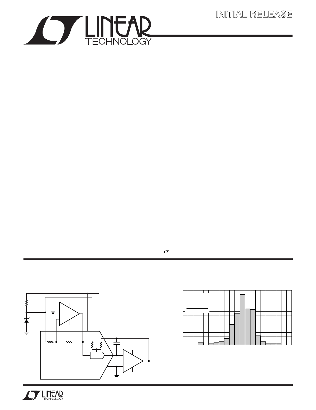
TYPICAL APPLICATIO
16-Bit Voltage Output DAC on ±5V Supply
1.65k
LT1634
4.096V
+
LT1881
–
5V
–5V
R
COM
LTC®1597
REFR1
U
TC VOS Distribution, Industrial Grade
5V
R
OFS
DAC
Information furnished by Linear Technology Corporation is believed to be accurate and reliable.
However, no responsibility is assumed for its use. Linear Technology Corporation makes no representation that the interconnection of its circuits as described herein will not infringe on existing patent rights.
33pF
–
+
LT1881
–5V
5V
V
OUT
–4.096V
TO 4.096V
1881/2 TA01
26
24
VS = ±15V
22
40 N8 (1 LOT)
20
144 S8 (2 LOTS)
18
184 TOTAL PARTS
16
14
12
10
8
PERCENT OF UNITS (%)
6
4
2
0
1 –0.8 –0.6 –0.4 –0.2 0 0.2 0.4 0.6 0.8–0.9 –0.7 –0.5 –0.3 –0.1 0.1 0.3 0.5 0.7 0.9 1
INPUT OFFSET VOLTAGE DRIFT (µV/°C)
1881/2 TA01a
1
Page 2
LT1881/LT1882
WW
W
ABSOLUTE AXI U RATI GS
U
(Note 1)
Supply Voltage (V+ to V–) ....................................... 40V
Differential Input Voltage (Note 2) .........................±10V
Input Voltage .................................................... V+ to V
Input Current (Note 2) ........................................ ±10mA
Output Short-Circuit Duration (Note 3)............ Indefinite
UUW
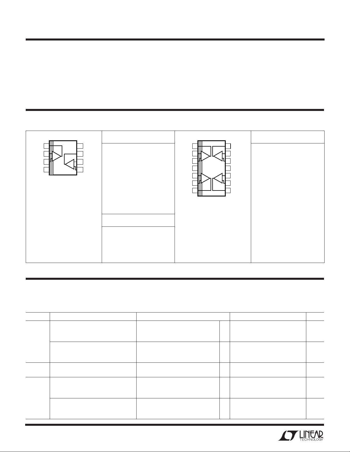
PACKAGE/ORDER I FOR ATIO
TOP VIEW
OUT A
1
–IN A
2
+IN A
N8 PACKAGE
8-LEAD PDIP
T
T
A
3
–
V
4
= 150°C, θJA = 130°C/W (N8)
JMAX
= 150°C, θJA = 190°C/W (S8)
JMAX
+
V
8
OUT B
7
–IN B
6
B
+IN B
5
S8 PACKAGE
8-LEAD PLASTIC SO
ORDER PART NUMBER
LT1881CN8
LT1881IN8
LT1881CS8
LT1881IS8
LT1881ACN8
LT1881AIN8
LT1881ACS8
LT1881AIS8
S8 PART MARKING
Operating Temperature Range (Note 4) .. –40°C to 85°C
Specified Temperature Range (Note 5)... – 40°C to 85°C
–
Maximum Junction Temperature .......................... 150°C
Storage Temperature Range ................. –65°C to 150°C
Lead Temperature (Soldering, 10 sec).................. 300°C
1
OUT A
2
–IN A
3
+IN A
+
4
V
5
+IN B
6
–IN B
7
OUT B
14-LEAD PLASTIC SO
T
JMAX
TOP VIEW
14
13
DA
12
11
10
DB
9
8
S PACKAGE
= 150°C, θJA = 150°C/W
OUT D
–IN D
+IN D
–
V
+IN C
–IN C
OUT C
ORDER PART NUMBER
LT1882CS
LT1882IS
1881
1881I
1881A
1881AI
Consult factory for Military grade parts.
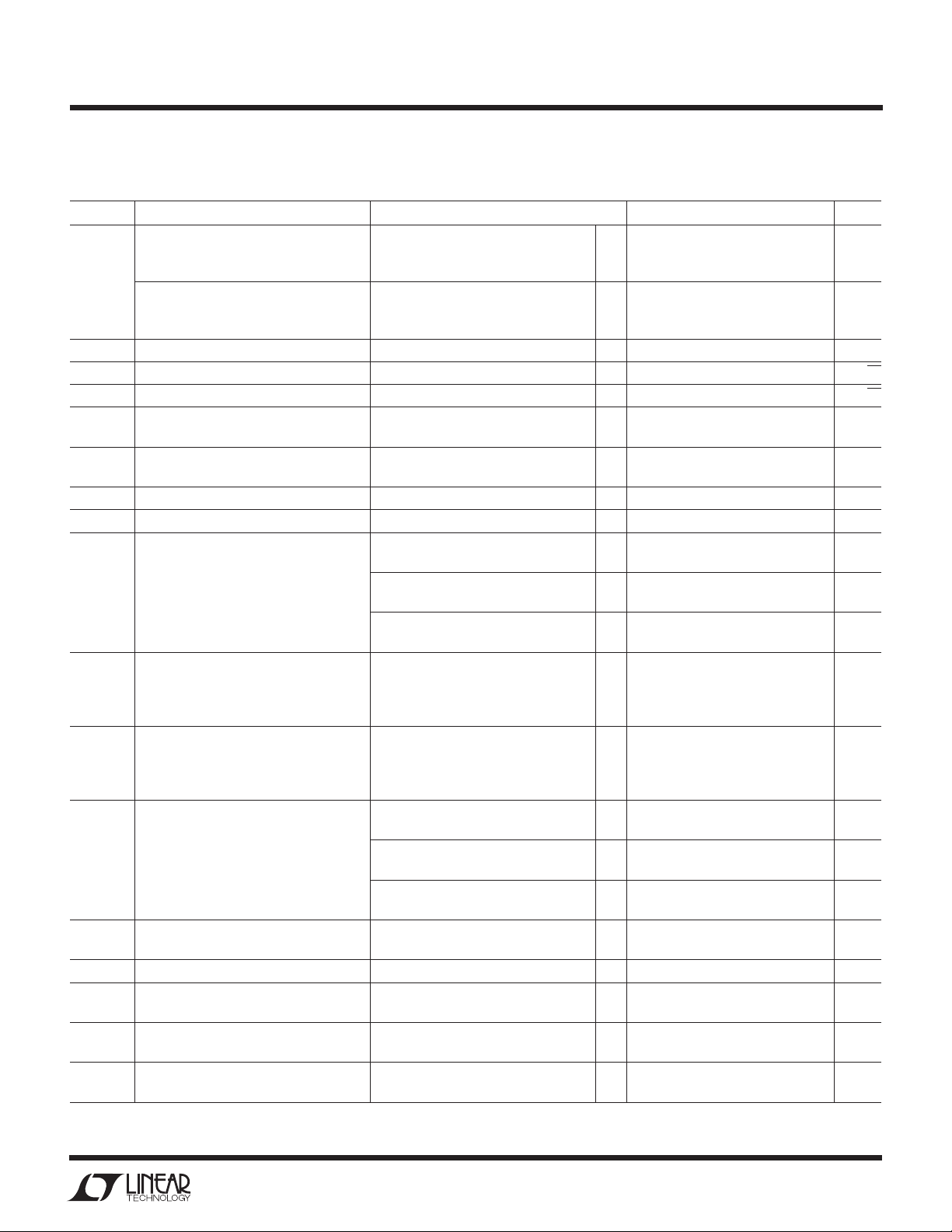
ELECTRICAL CHARACTERISTICS
The ● denotes the specifications which apply over the full operating temperature range, otherwise specifications are at TA = 25°C.
Single supply operation VEE = 0, VCC = 5V; VCM = VCC/2 unless otherwise noted. (Note 5)
SYMBOL PARAMETER CONDITIONS MIN TYP MAX UNITS
V
OS
I
OS
Input Offset Voltage (LT1881A) 25 50 µV
< 70°C ● 85 µV
0°C < T
A
–40°C < T
Input Offset Voltage (LT1881/LT1882) 30 80 µV
0°C < T
–40°C < T
Input Offset Voltage Drift 0°C < TA < 70°C ● 0.3 0.8 µV/°C
(Note 6) –40°C < T
Input Offset Current (LT1881A) 100 200 pA
0°C < T
–40°C < T
Input Offset Current (LT1881/LT1882) 150 500 pA
0°C < T
–40°C < T
< 85°C ● 110 µV
A
< 70°C ● 125 µV
A
< 85°C ● 150 µV
A
< 85°C ● 0.3 0.8 µV/°C
A
< 70°C ● 250 pA
A
< 85°C ● 300 pA
A
< 70°C ● 600 pA
A
< 85°C ● 700 pA
A
2
Page 3
LT1881/LT1882
ELECTRICAL CHARACTERISTICS
The ● denotes the specifications which apply over the full operating temperature range, otherwise specifications are at TA = 25°C.
Single supply operation VEE = 0, VCC = 5V; VCM = VCC/2 unless otherwise noted. (Note 5)
SYMBOL PARAMETER CONDITIONS MIN TYP MAX UNITS
I
B
e
n
i
n
V
CM
CMRR Common Mode Rejection Ratio 1V < VCM < 4V 106 128 dB
PSRR Power Supply Rejection Ratio VEE = 0, VCM = 1.5V; 2.7V < VCC < 32V ● 106 132 dB
A
VOL
V
OL
V
OH
I
S
I
SC
GBW Gain-Bandwidth Product f = 20kHz 0.5 1.0 MHz
t
S
+
SR
–
SR
Input Bias Current (LT1881A) 100 200 pA
< 70°C ● 250 pA
0°C < T
A
–40°C < T
< 85°C ● 300 pA
A
Input Bias Current (LT1881/LT1882) 150 500 pA
< 70°C ● 600 pA
0°C < T
A
–40°C < T
Input Noise Voltage 0.1Hz to 10Hz 0.5 µV
< 85°C ● 700 pA
A
P-P
Input Noise Voltage Density f = 1kHz 14 nV/√Hz
Input Noise Current Density f = 1kHz 0.03 pA/√Hz
Input Voltage Range VEE + 1.0 VCC – 1.0 V
1.2V < V
● V
< 3.8V ● 104 dB
CM
+ 1.2 VCC – 1.2 V
EE
Minimum Operating Supply Voltage ● 2.4 2.7 V
Large-Signal Voltage Gain RL = 10k; 1V < V
RL = 2k; 1V < V
RL = 1k; 1V < V
< 4V 500 1600 V/mV
OUT
< 4V 300 800 V/mV
OUT
< 4V 250 400 V/mV
OUT
● 350 V/mV
● 250 V/mV
● 200 V/mV
Output Voltage Swing Low No Load ● 20 40 mV
I
= 100µA ● 25 50 mV
SINK
= 1mA ● 70 150 mV
I
SINK
= 5mA ● 270 600 mV
I
SINK
Output Voltage Swing High No Load ● 120 220 mV
(Referred to V
)I
CC
= 100µA ● 130 230 mV
SOURCE
I
= 1mA ● 180 300 mV
SOURCE
= 5mA ● 360 600 mV
I
SOURCE
Supply Current Per Amplifier VCC = 3V 0.45 0.65 0.85 mA
● 1.2 mA
VCC = 5V 0.5 0.65 0.9 mA
● 1.4 mA
VCC = 12V 0.5 0.70 1.0 mA
● 1.5 mA
Short-Circuit Current V
Settling Time 0.01%, V
Short to GND ● 15 30 mA
OUT
Short to V
V
OUT
= –1, RL = 2k
A
V
CC
= 1.5V to 3.5V, 30 µs
OUT
● 15 30 mA
Slew Rate Positive AV = –1 0.15 0.35 V/µs
● 0.12 V/µs
Slew Rate Negative AV = –1 0.11 0.18 V/µs
● 0.08 V/µs
3
Page 4
LT1881/LT1882
ELECTRICAL CHARACTERISTICS
The ● denotes the specifications which apply over the full operating temperature range, otherwise specifications are at TA = 25°C.
Single supply operation VEE = 0, VCC = 5V; VCM = VCC/2 unless otherwise noted. (Note 5)
SYMBOL PARAMETER CONDITIONS MIN TYP MAX UNITS
∆V
OS
∆IB+ Noninverting Bias Current Match (Notes 7, 8) 200 300 pA
∆CMRR Common Mode Rejection Match (Notes 7, 9) ● 102 125 dB
∆PSRR Power Supply Rejection Match VEE = 0V, VCM = 1.5V, 2.7V < VCC < 32V, ● 104 126 dB
Offset Voltage Match (LT1881A) (Note 7) 30 70 µV
0°C < T
< 70°C ● 125 µV
A
–40°C < T
< 85°C ● 160 µV
A
Offset Voltage Match (LT1881/LT1882) (Note 7) 35 125 µV
< 70°C ● 175 µV
0°C < T
A
–40°C < T
< 85°C ● 235 µV
A
Offset Voltage Match Drift (Notes 6, 7) ● 0.4 1.2 µV/°C
(LT1881A) 0°C < T
< 70°C ● 400 pA
A
–40°C < T
< 85°C ● 500 pA
A
Noninverting Bias Current Match (Notes 7, 8) 250 700 pA
(LT1881/LT1882) 0°C < T
< 70°C ● 900 pA
A
–40°C < T
< 85°C ● 1000 pA
A
(Notes 7, 9)
The ● denotes the specifications which apply over the full operating temperature range, otherwise specifications are at TA = 25°C.
Split supply operation VS = ±15V, VCM = 0V unless otherwise noted. (Note 5)
SYMBOL PARAMETER CONDITIONS MIN TYP MAX UNITS
V
OS
I
OS
I
B
e
n
i
n
V
CM
Input Offset Voltage (LT1881A) 25 50 µV
< 70°C ● 85 µV
0°C < T
A
–40°C < T
< 85°C ● 110 µV
A
Input Offset Voltage (LT1881/LT1882) 30 80 µV
0°C < T
< 70°C ● 125 µV
A
–40°C < T
< 85°C ● 150 µV
A
Input Offset Voltage Drift 0°C < TA < 70°C ● 0.3 0.8 µV/°C
(Note 6) –40°C < T
< 85°C ● 0.3 0.8 µV/°C
A
Input Offset Current (LT1881A) 150 200 pA
< 70°C ● 250 pA
0°C < T
A
–40°C < T
< 85°C ● 300 pA
A
Input Offset Current (LT1881/LT1882) 150 500 pA
< 70°C ● 600 pA
0°C < T
A
–40°C < T
< 85°C ● 700 pA
A
Input Bias Current (LT1881A) 150 200 pA
0°C < T
< 70°C ● 250 pA
A
–40°C < T
< 85°C ● 300 pA
A
Input Bias Current (LT1881/LT1882) 150 500 pA
< 70°C ● 600 pA
0°C < T
A
–40°C < T
Input Noise Voltage 0.1Hz to 10Hz 0.5 µV
< 85°C ● 700 pA
A
P-P
Input Noise Voltage Density f = 1kHz 14 nV/√Hz
Input Noise Current Density f = 1kHz 0.03 pA/√Hz
Input Voltage Range VEE + 1.0 VCC – 1.0 V
● V
+ 1.2 VCC – 1.2 V
EE
4
Page 5

LT1881/LT1882
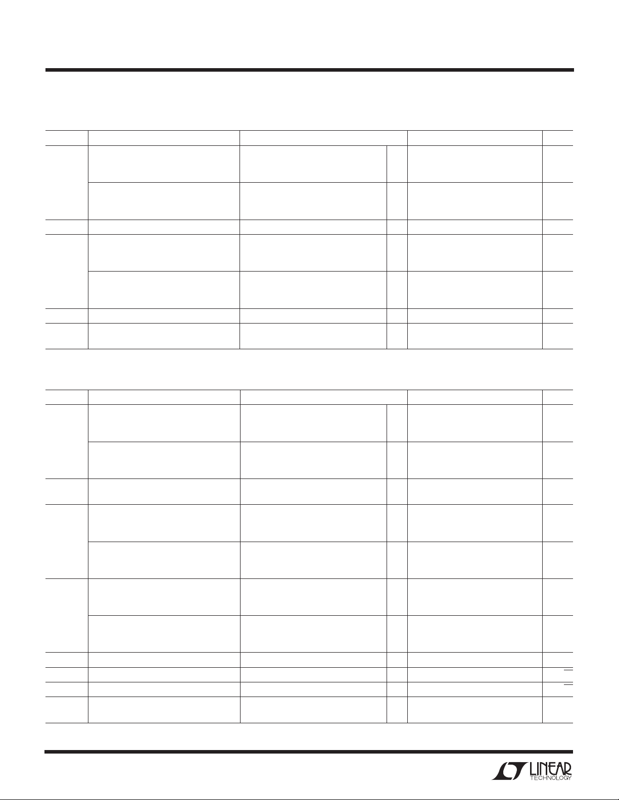
ELECTRICAL CHARACTERISTICS
The ● denotes the specifications which apply over the full operating temperature range, otherwise specifications are at TA = 25°C.
Split supply operation VS = ±15V, VCM = 0V unless otherwise noted. (Note 5)
SYMBOL PARAMETER CONDITIONS MIN TYP MAX UNITS
CMRR Common Mode Rejection Ratio –13.5V < VCM < 13.5V ● 114 130 dB
+PSRR Positive Power Supply Rejection Ratio VEE = –15, VCM = 0; 1.5V < VCC < 18V ● 110 132 dB
–PSRR Negative Power Supply Rejection Ratio VCC = 15, VCM = 0; –1.5V < VEE < –18V ● 106 132 dB
Minimum Operating Supply Voltage ● ±1.2 ±1.35 V
A
VOL
V
OL
V
OH
I
S
I
SC
GBW Gain-Bandwidth Product f = 20kHz 0.6 1.1 MHz
t
S
+
SR
–
SR
∆V
OS
∆IB+ Noninverting Bias Current Match (Notes 7, 8) 240 700 pA
∆CMRR Common Mode Rejection Match (Notes 7, 9) ● 110 125 dB
Large-Signal Voltage Gain RL = 10k; –13.5V < V
RL = 2k; –13.5V < V
RL = 1k; –12V < V
< 13.5V 1000 1600 V/mV
OUT
< 13.5V 175 420 V/mV
OUT
< 12V 90 230 V/mV
OUT
● 700 V/mV
● 125 V/mV
● 65 V/mV
Output Voltage Swing Low No Load ● 20 40 mV
(Referred to V
)I
EE
= 100µA ● 25 50 mV
SINK
= 1mA ● 70 150 mV
I
SINK
= 5mA ● 270 600 mV
I
SINK
Output Voltage Swing High No Load ● 160 220 mV
(Referred to V
)I
CC
= 100µA ● 160 230 mV
SOURCE
I
= 1mA ● 180 300 mV
SOURCE
= 5mA ● 360 600 mV
I
SOURCE
Supply Current Per Amplifier VS = ±15V 0.5 0.85 1.1 mA
● 1.6 mA
Short-Circuit Current V
Settling Time 0.01%, V
Short to V
OUT
V
Short to V
OUT
= –1, RL = 2k
A
V
EE
CC
= –5V to 5V, 35 µs
OUT
● 15 40 mA
● 15 30 mA
20 40 mA
20 30 mA
Slew Rate Positive AV = –1 0.21 0.4 V/µs
● 0.18 V/µs
Slew Rate Negative AV = –1 0.13 0.20 V/µs
● 0.1 V/µs
Offset Voltage Match (LT1881/LT1882) (Note 5) 42 125 µV
< 70°C ● 175 µV
0°C < T
A
–40°C < T
< 85°C ● 235 µV
A
Offset Voltage Match (LT1881A) 35 70 µV
< 70°C ● 125 µV
0°C < T
A
–40°C < T
< 85°C ● 160 µV
A
Offset Voltage Match Drift (Notes 6, 7) ● 0.4 1.1 µV/°C
(LT1881/LT1882) 0°C < T
< 70°C ● 900 pA
A
–40°C < T
< 85°C ● 1000 pA
A
Noninverting Bias Current Match 200 300 pA
(LT1881A) 0°C < T
< 70°C ● 400 pA
A
–40°C < T
< 85°C ● 500 pA
A
5
Page 6

LT1881/LT1882
ELECTRICAL CHARACTERISTICS
The ● denotes the specifications which apply over the full operating temperature range, otherwise specifications are at TA = 25°C.
Split supply operation VS = ±15V, VCM = 0V unless otherwise noted. (Note 5)
SYMBOL PARAMETER CONDITIONS MIN TYP MAX UNITS
∆+PSRR Positive Power Supply Rejection Match VEE = –15V, VCM = 0V, ● 108 130 dB
1.5V < V
∆–PSRR Negative Power Supply Rejection Match VCC = 15V, VCM = 0V, ● 104 130 dB
–1.5V < V
Note 1: Absolute Maximum Ratings are those values beyond which the life
of a device may be impaired.
Note 2: The inputs are protected by internal resistors and back-to-back
diodes. If the differential input voltage exceeds ±0.7V, the input current
should be limited externally to less than 10mA.
Note 3: A heat sink may be required to keep the junction temperature
below absolute maximum.
Note 4: The LT1881C, LT1882C, LT1881I and LT1882I are guaranteed
functional over the operating temperature range of –40°C to 85°C.
Note 5: The LT1881C and LT1882C are designed, characterized and
expected to meet specified performance from –40°C to 85°C but are not
tested or QA sampled at these temperatures. The LT1881I and LT1882I are
guaranteed to meet specified performance from –40°C to 85°C.
< 18V, (Notes 7, 9)
CC
< –18V, (Notes 7, 9)
EE
Note 6: This parameter is not 100% tested.
Note 7: Matching parameters are the difference between amplifiers
A and B in the LT1881; and between amplifiers A and D and B and C in the
LT1882.
Note 8: This parameter is the difference between the two noninverting
input bias currents.
Note 9: ∆CMRR and ∆PSRR are defined as follows: CMRR and PSRR are
measured in µV/V on each amplifier. The difference is calculated in µV/V
and then converted to dB.
UW
TYPICAL PERFOR A CE CHARACTERISTICS
Supply Current per Amplifier vs
Supply Voltage Slew Rate vs Supply Voltage Slew Rate vs Temperature
1200
1000
800
600
400
200
SUPPLY CURRENT PER AMPLIFIER (µA)
0
0 4 8 12 16 20 24 28 32 36
TOTAL SUPPLY VOLTAGE (V)
125°C
25°C
–55°C
1881/2 G01
SLEW RATE (V/µs)
0.45
AV = –1
0.40
0.35
0.30
0.25
0.20
0.15
0.10
0.05
0
4 8 12 16 20 24 28 32 36
0
RISING
FALLING
TOTAL SUPPLY VOLTAGE (V)
1881/2 G02
0.5
0.4
0.3
0.2
SLEW RATE (V/µs)
0.1
0
–25 0 25 50 75 100 125 150
–50
TEMPERATURE (°C)
RISING
FALLING
VS = ±15V
VS = ±5V
VS = ±15V
VS = ±5V
1881/2 G03
6
Page 7

LT1881/LT1882
UW
TYPICAL PERFOR A CE CHARACTERISTICS
Gain Bandwidth Product vs
Settling Time vs Output Step Settling Time vs Output Step
10
VS = ±15V
8
A
= –1
V
6
4
2
0
–2
OUTPUT STEP (V)
–4
–6
–8
–10
0.1% 0.01%
0.1% 0.01%
5 10 15 20 25 30 35 40 45 50 55 60 65
0
SETTLING TIME (µs)
1881/2 G04
10
VS = ±15V
8
A
= 1
V
6
4
0.1% 0.01%
2
0
–2
OUTPUT STEP (V)
–4
–6
–8
–10
0.1% 0.01%
5 10 15 20 25 30 35 40 45 50 55 60 65
0
SETTLING TIME (µs)
1881/2 G05
Phase Margin vs Supply Voltage Gain vs Frequency, AV = –1 Gain vs Frequency, AV = 1
60
10
Supply Voltage
900
850
800
750
700
650
GAIN BANDWIDTH PRODUCT (kHz)
600
4 8 12 16 20 24 28 32 36
0
TOTAL SUPPLY VOLTAGE (V)
10
125°C
25°C
–55°C
1881/2 G06
58
56
54
52
PHASE MARGIN (DEG)
50
48
46
4 8 12 16 20 24 28 32 36
0
TOTAL SUPPLY VOLTAGE (V)
10
0
–10
GAIN (dB)
–20
–55°C
125°C
125°C
1881/2 G07
Gain vs Frequency with C
AV = 1
VS = ±15V
LOAD
1500pF
1000pF
500pF
,
0pF
0
–10
GAIN (dB)
–20
–30
–40
1k
VS = ±15VVS = ±2.5V
10k 100k 1M 10M 100M
FREQUENCY (Hz)
1881/2 G08
Gain vs Frequency with C
AV = –1
10
0
–10
GAIN (dB)
–20
GAIN (dB)
VS = ±15V
–10
–20
–30
–40
0
10k 100k 1M 10M 100M
1k
FREQUENCY (Hz)
,
LOAD
1800pF
1000pF
500pF
VS = ±15VVS = ±2.5V
1881/2 G09
–30
–40
10k 100k 1M 10M 100M
1k
FREQUENCY (Hz)
1881/2 G10
–30
–40
10k 100k 1M 10M 100M
1k
FREQUENCY (Hz)
0pF
1881/2 G11
7
Page 8

LT1881/LT1882
UW
TYPICAL PERFOR A CE CHARACTERISTICS
Large Signal Response, AV = –1
Large Signal Response, AV = 1
Small Signal Response, AV = –1,
No Load
(5V/DIV)
OUT
V
TIME (50µs/DIV) 1881/2 G12
Small Signal Response, AV = –1,
CL = 1000pF
(20mV/DIV)
OUT
V
TIME (2µs/DIV) 1881/2 G15
(5V/DIV)
OUT
V
TIME (50µs/DIV) 1881/2 G13
Small Signal Response, AV = 1,
RL = 2k
(20mV/DIV)
OUT
V
TIME (2µs/DIV) 1881/2 G16
(20mV/DIV)
OUT
V
TIME (2µs/DIV) 1881/2 G14
Small Signal Response, AV = 1,
CL = 500pF
(20mV/DIV)
OUT
V
TIME (2µs/DIV) 1881/2 G17
8
Page 9

LT1881/LT1882
U
WUU
APPLICATIO S I FOR ATIO
The LT1881 dual and LT1882 quad op amps feature
exceptional input precision with rail-to-rail output swing.
The amplifiers are similar to the LT1884 and LT1885
devices. The LT1881 and LT1882 offer superior capacitive
load driving capabilities over the LT1884 and LT1885 in
low voltage gain configurations. Offset voltages are trimmed
to less than 50µV and input bias currents are less than
200pA on the “A” grade devices. Obtaining beneficial
advantage of these precision input characteristics depends upon proper applications circuit design and board
layout.
Preserving Input Precision
Preserving the input voltage accuracy of the LT1881/
LT1882 requires that the applications circuit and PC board
layout do not introduce errors comparable to or greater
than the 30µV offset. Temperature differentials across the
input connections can generate thermocouple voltages of
10’s of microvolts. PC board layouts should keep connections to the amplifier’s input pins close together and away
from heat dissipating components. Air currents across the
board can also generate temperature differentials.
The extremely low input bias currents, 150pA, allow high
accuracy to be maintained with high impedance sources
and feedback networks. The LT1881/LT1882’s low input
bias currents are obtained by using a cancellation circuit
on-chip. This causes the resulting I
uncorrelated, as implied by the IOS specification being
greater than the I
the input resistances in each input lead, as is commonly
recommended with most amplifiers. The impedance at
either input should be kept as small as possible to minimize total circuit error.
. The user should not try to balance
BIAS
BIAS
+ and I
BIAS
– to be
PC board layout is important to insure that leakage currents do not corrupt the low I
precision, high impedance circuits, the input pins should
be surrounded by a guard ring of PC board interconnect,
with the guard driven to the same common mode voltage
as the amplifier inputs.
Input Common Mode Range
The LT1881 and LT1882 outputs are able to swing nearly
to each power supply rail, but the input stage is limited to
operating between VEE + 0.8V and VCC – 0.9V. Exceeding
this common mode range will cause the gain to drop to
zero; however, no gain reversal will occur.
Input Protection
The inverting and noninverting input pins of the LT1881
and LT1882 have limited on-chip protection. ESD protection is provided to prevent damage during handling. The
input transistors have voltage clamping and limiting resistors to protect against input differentials up to 10V. Short
transients above this level will also be tolerated. If the input
pins can see a sustained differential voltage above 10V,
external limiting resistors should be used to prevent
damage to the amplifier. A 1k resistor in each input lead
will provide protection against a 30V differential voltage.
Capacitive Loads
The LT1881 and LT1882 can drive capacitive loads up to
1000pF in unity-gain. The capacitive load driving increases as the amplifier is used in higher gain configurations. Capacitive load driving may be increased by
decoupling the capacitance from the output with a small
resistance.
of the amplifier. In high
BIAS
9
Page 10

LT1881/LT1882
PACKAGE DESCRIPTIO
U
Dimensions in inches (millimeters) unless otherwise noted.
N8 Package
8-Lead PDIP (Narrow 0.300)
(LTC DWG # 05-08-1510)
0.400*
(10.160)
MAX
876
0.255 ± 0.015*
(6.477 ± 0.381)
5
12
0.300 – 0.325
(7.620 – 8.255)
0.065
(1.651)
0.009 – 0.015
(0.229 – 0.381)
+0.035
0.325
–0.015
+0.889
8.255
()
–0.381
*THESE DIMENSIONS DO NOT INCLUDE MOLD FLASH OR PROTRUSIONS.
MOLD FLASH OR PROTRUSIONS SHALL NOT EXCEED 0.010 INCH (0.254mm)
TYP
0.045 – 0.065
(1.143 – 1.651)
0.100
(2.54)
BSC
3
4
0.130 ± 0.005
(3.302 ± 0.127)
0.125
(3.175)
MIN
0.018 ± 0.003
(0.457 ± 0.076)
0.020
(0.508)
MIN
N8 1098
10
Page 11

PACKAGE DESCRIPTIO
LT1881/LT1882
U
Dimensions in inches (millimeters) unless otherwise noted.
S8 Package
8-Lead Plastic Small Outline (Narrow 0.150)
(LTC DWG # 05-08-1610)
0.189 – 0.197*
(4.801 – 5.004)
7
8
5
6
0.228 – 0.244
(5.791 – 6.197)
0.010 – 0.020
(0.254 – 0.508)
0.008 – 0.010
(0.203 – 0.254)
*
DIMENSION DOES NOT INCLUDE MOLD FLASH. MOLD FLASH
SHALL NOT EXCEED 0.006" (0.152mm) PER SIDE
**
DIMENSION DOES NOT INCLUDE INTERLEAD FLASH. INTERLEAD
FLASH SHALL NOT EXCEED 0.010" (0.254mm) PER SIDE
×
°
45
0.016 – 0.050
(0.406 – 1.270)
0°– 8° TYP
S Package
14-Lead Plastic Small Outline (Narrow 0.150)
(LTC DWG # 05-08-1610)
0.053 – 0.069
(1.346 – 1.752)
0.014 – 0.019
(0.355 – 0.483)
TYP
13
14
1
0.337 – 0.344*
(8.560 – 8.738)
12
0.150 – 0.157**
(3.810 – 3.988)
3
2
4
0.004 – 0.010
(0.101 – 0.254)
0.050
(1.270)
BSC
SO8 1298
11
10
8
9
0.228 – 0.244
(5.791 – 6.197)
0.010 – 0.020
(0.254 – 0.508)
0.008 – 0.010
(0.203 – 0.254)
*
DIMENSION DOES NOT INCLUDE MOLD FLASH. MOLD FLASH
SHALL NOT EXCEED 0.006" (0.152mm) PER SIDE
**
DIMENSION DOES NOT INCLUDE INTERLEAD FLASH. INTERLEAD
FLASH SHALL NOT EXCEED 0.010" (0.254mm) PER SIDE
× 45°
0° – 8° TYP
0.016 – 0.050
(0.406 – 1.270)
0.053 – 0.069
(1.346 – 1.752)
0.014 – 0.019
(0.355 – 0.483)
TYP
0.150 – 0.157**
(3.810 – 3.988)
1
3
2
4
5
0.050
(1.270)
BSC
7
6
0.004 – 0.010
(0.101 – 0.254)
S14 1298
11
Page 12

LT1881/LT1882
TYPICAL APPLICATIO
10k
0.1%
10k
0.1%
U
–50°C to 600°C Digital Thermometer Operates on 3.3V
= 3.3V
V
CC
R
F
1k
V
CC
–
A1
1/2 LT1881
+
R1
4k
R
T
R2
4k
R3
1k
V
CC
–
A2
1/2 LT1881
+
V
CC
V = + 1.588mV/°C
2
RT: OMEGA F4132 1000Ω RTD
R1, R2, R3, RF: USE BI 698-3 2k × 8 RESISTOR NETWORK
V
REF
+IN CLK
LTC1287
–IN D
GND CS/SHDN
V
OUT
CC
1µF
1881/2 TA02
RELATED PARTS
PART NUMBER DESCRIPTION COMMENTS
LT1112/LT1114 Dual/Quad Picoamp Input Op Amp VOS = 60µV Max
LT1677 Gain Programmable Instrumentation Amp Gain Error = 0.08% Max
LT1793 Low Noise JFET Op Amp IB = 10pA Max
LT1884/LT1885 Dual/Quad Picoamp Input Op Amp 3 Times Faster than LT1881/LT1882
LTC2050 Zero Drift Op Amp in SOT-23 VOS = 3µV Max, Rail-to-Rail Output
12
Linear Technology Corporation
1630 McCarthy Blvd., Milpitas, CA 95035-7417
(408) 432-1900 ● FAX: (408) 434-0507
●
www.linear-tech.com
18812i LT/TP 0400 4K • PRINTED IN USA
LINEAR TECHNOLOGY CORPORATION 2000
 Loading...