

Page 1
FEATURES
LT1795
Dual 500mA/50MHz
Current Feedback Line Driver
Amplifier
U
DESCRIPTIO
■
500mA Output Drive Current
■
50MHz Bandwidth, AV = 2, RL = 25
■
900V/µs Slew Rate, AV = 2, RL = 25
■
Low Distortion: –75dBc at 1MHz
■
High Input Impedance, 10MΩ
■
Wide Supply Range, ±5V to ±15V
■
Full Rate, Downstream ADSL Supported
■
Power Enhanced Small Footprint Packages
Ω
Ω
TSSOP-20, S0-20 Wide
■
Low Power Shutdown Mode
■
Power Saving Adjustable Supply Current
■
Stable with CL = 10,000pF
U
APPLICATIO S
■
ADSL HDSL2, G.lite Drivers
■
Buffers
■
Test Equipment Amplifiers
■
Video Amplifiers
■
Cable Drivers
U
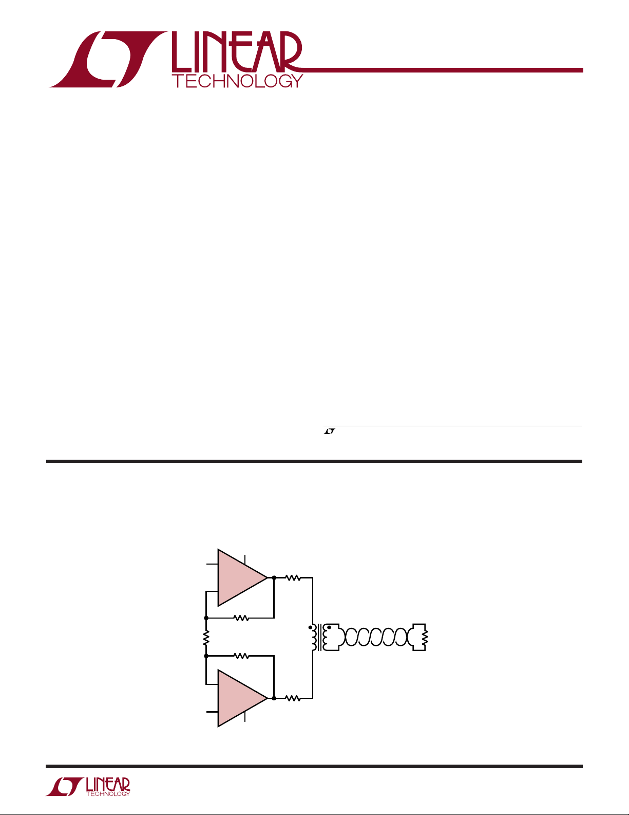
TYPICAL APPLICATION
The LT®1795 is a dual current feedback amplifier with high
output current and excellent large signal characteristics.
The combination of high slew rate, 500mA output drive
and up to ±15V operation enables the device to deliver
significant power at frequencies in the 1MHz to 2MHz
range. Short-circuit protection and thermal shutdown
insure the device’s ruggedness. The LT1795 is stable with
large capacitive loads and can easily supply the large
currents required by the capacitive loading. A shutdown
feature switches the device into a high impedance, low
current mode, reducing power dissipation when the device is not in use. For lower bandwidth applications, the
supply current can be reduced with a single external
resistor.
The LT1795 comes in the very small, thermally enhanced,
20-lead TSSOP package for maximum port density in line
driver applications.
, LTC and LT are registered trademarks of Linear Technology Corporation.
Low Loss, High Power Central Office ADSL Line Driver
+
V
+IN
+
1/2
LT1795
–
1k
165Ω
1k
–
1/2
–IN
* MIDCOM 50215 OR EQUIVALENT
LT1795
+
–
V
12.5Ω
1:2*
12.5Ω
100Ω
1795 TA01
1
Page 2

LT1795
WW
W
ABSOLUTE AXI U RATI GS
U
(Note 1)
Supply Voltage ...................................................... ±18V
Input Current ...................................................... ±15mA
Output Short-Circuit Duration (Note 2)............ Indefinite
Operating Temperature Range ................ –40°C to 85°C
UUW
PACKAGE/ORDER I FOR ATIO
–IN
+IN
SHDN
SHDNREF
+IN
–IN
TOP VIEW
–
1
V
2
NC
3
4
5
6
7
8
9
NC
–
10
V
FE PACKAGE
20-LEAD PLASTIC TSSOP
T
= 150° C, θJA = 40°C/W (Note 4)
JMAX
–
20
V
19
NC
18
OUT
+
17
V
16
COMP
15
COMP
+
14
V
13
OUT
12
NC
–
11
V
ORDER PART
NUMBER
LT1795CFE
LT1795IFE
Specified Temperature Range (Note 3)... – 40°C to 85°C
Junction Temperature........................................... 150°C
Storage Temperature Range ................. –65°C to 150°C
Lead Temperature (Soldering, 10 sec).................. 300°C
TOP VIEW
1
COMP
+
2
V
3
OUT
–
4
V
–
5
V
–
6
V
–
7
V
8
–IN
9
+IN
10
SHDN
S PACKAGE
20-LEAD PLASTIC SW
T
= 150° C, θJA ≈ 40°C/W (Note 4)
JMAX
20
19
18
17
16
15
14
13
12
11
COMP
+
V
OUT
–
V
–
V
–
V
–
V
–IN
+IN
SHDNREF
ORDER PART
NUMBER
LT1795CSW
LT1795ISW
Consult factory for Military grade parts.
ELECTRICAL CHARACTERISTICS
The ● denotes the specifications which apply over the full specified temperature range, otherwise specifications are at TA = 25°C.
VCM = 0V, ±5V ≤ VS ≤ ±15V, pulse tested, V
SYMBOL PARAMETER CONDITIONS MIN TYP MAX UNITS
V
I
I
e
+i
–i
OS
+
IN
–
IN
n
n
n
Input Offset Voltage ±3 ±13 mV
Input Offset Voltage Matching ±1 ±3.5 mV
Input Offset Voltage Drift ● 10 µV/°C
Noninverting Input Current ±2 ±5 µA
Noninverting Input Current Matching ±0.5 ±2 µA
Inverting Input Current ±10 ±70 µA
Inverting Input Current Matching ±10 ±30 µA
Input Noise Voltage Density f = 10kHz, RF =1k, RG = 10Ω, RS = 0Ω 3.6 nV/√Hz
Input Noise Current Density f = 10kHz, RF =1k, RG = 10Ω, RS = 10kΩ 2 pA/√Hz
Input Noise Current Density f = 10kHz, RF =1k, RG = 10Ω, RS = 10kΩ 30 pA/√Hz
SHDN
= 2.5V, V
SHDNREF
= 0V unless otherwise noted. (Note 3)
● ±4.5 ±17 mV
● ±1.5 ±5.0 mV
● ±8 ±20 µA
● ±1.5 ±7 µA
● ±20 ±100 µA
● ±20 ±50 µA
2
Page 3
LT1795
ELECTRICAL CHARACTERISTICS
The ● denotes the specifications which apply over the full specified temperature range, otherwise specifications are at TA = 25°C.
VCM = 0V, ±5V ≤ VS ≤ ±15V, pulse tested, V
SYMBOL PARAMETER CONDITIONS MIN TYP MAX UNITS
+
R
IN
+
C
IN
CMRR Common Mode Rejection Ratio VS = ±15V, VCM = ±12V ● 55 62 dB
PSRR Power Supply Rejection Ratio VS = ±5V to ±15V ● 60 77 dB
A
V
R
OL
V
OUT
I
OUT
I
S
HD2, HD
3
SR Slew Rate (Note 7) AV = 4, RL = 400Ω 400 900 V/µs
BW Small-Signal BW AV = 2, VS = ±15V, Peaking ≤ 1.5dB 65 MHz
Input Resistance VIN = ±12V, VS = ±15V ● 1.5 10 MΩ
Input Capacitance VIN = ±15V 2 pF
Input Voltage Range (Note 5) VS = ±15V ● ±12 ±13.5 V
Inverting Input Current VS = ±15V, VCM = ±12V ● 110µA/V
Common Mode Rejection V
Noninverting Input Current VS = ±5V to ±15V ● 30 500 nA/V
Power Supply Rejection
Inverting Input Current VS = ±5V to ±15V ● 15µA/V
Power Supply Rejection
Large-Signal Voltage Gain VS = ±15V, V
Transresistance, ∆V
OUT
/∆I
–
IN
Maximum Output Voltage Swing VS = ±15V, RL = 25Ω±11.5 ±12.5 V
Maximum Output Current VS = ±15V, RL = 1Ω ● 0.5 1 A
Supply Current Per Amplifier VS = ±15V, V
Supply Current Per Amplifier, VS = ±15V 15 20 mA
= 51k, (Note 6) ● 25 mA
R
SHDN
Positive Supply Current, Shutdown VS = ±15V, V
Output Leakage Current, Shutdown VS = ±15V, V
Channel Separation VS = ±15V, V
2nd and 3rd Harmonic Distortion f = 1MHz, VO = 20V
Differential Mode
Slew Rate AV = 4, RL = 25Ω 900 V/µs
SHDN
= 2.5V, V
SHDNREF
= 0V unless otherwise noted. (Note 3)
V = ±2V, VS = ±5V ● 0.5 5 MΩ
VS = ±5V ● ±2 ±3.5 V
VS = ±5V, VCM = ±2V ● 50 60 dB
= ±5V, VCM = ±2V ● 110µA/V
S
= ±10V, RL = 25Ω ● 55 68 dB
= ±5V, V
V
S
VS = ±15V, V
VS = ±5V, V
OUT
= ±2V, RL = 12Ω ● 55 68 dB
OUT
= ±10V, RL = 25Ω ● 75 200 kΩ
OUT
= ±2V, RL = 12Ω ● 75 200 kΩ
OUT
● ±10.0 ±11.5 V
VS = ±5V, RL = 12Ω±2.5 ±3V
● ±2.0 ±3V
= 2.5V 29 34 mA
SHDN
= 0.4V ● 1 200 µA
SHDN
= 0.4V 1 10 µA
SHDN
= ±10V, RL = 25Ω 80 110 dB
OUT
, RL = 50, AV = 2 –75 dBc
P-P
● 42 mA
RF = RG = 910Ω, RL = 100Ω
AV = 2, VS = ±15V, Peaking ≤ 1.5dB 50 MHz
= RG = 820Ω, RL = 25Ω
R
F
Note 1: Absolute Maximum Ratings are those values beyond which the life
of a device may be impaired.
Note 2: Applies to short-circuits to ground only. A short-circuit between
the output and either supply may permanently damage the part when
operated on supplies greater than ±10V.
Note 3: The LT1795C is guaranteed to meet specified performance from
0°C to 70°C and is designed, characterized and expected to meet these
extended temperature limits, but is not tested at –40°C and 85°C. The
LT1795I is guaranteed to meet the extended temperature limits.
Note 4: Thermal resistance varies depending upon the amount of PC board
metal attached to the device. If the maximum dissipation of the package is
exceeded, the device will go into thermal shutdown and be protected.
Note 5: Guaranteed by the CMRR tests.
Note 6: R
is connected between the SHDN pin and V+.
SHDN
Note 7: Slew rate is measured at ±5V on a ±10V output signal while
operating on ±15V supplies with R
R
= 400Ω.
L
= 1k, RG = 333Ω (AV = +4) and
F
3
Page 4
LT1795
W
UU
SMALL-SIGNAL BANDWIDTH
RSD = 0Ω, IS = 30mA per Amplifer, VS = ±15V,
Peaking ≤ 1dB, RL = 25Ω
A
V
R
F
–1 976 976 44
1 1.15k — 53
2 976 976 48
10 649 72 46
R
G
–3dB BW
(MHz)
RSD = 51kΩ, IS = 15mA per Amplifer, VS = ±15V,
Peaking ≤ 1dB, RL = 25Ω
A
V
–1 976 976 30
1 1.15k — 32
2 976 976 32
10 649 72 27
UW
TYPICAL PERFOR A CE CHARACTERISTICS
Supply Current vs Ambient
Temperature
40
VS = ±15V
= 1
A
35
V
= ∞
R
L
30
25
20
15
10
5
SUPPLY CURRENT PER AMPLIFIER (mA)
0
–50
–25 0
TEMPERATURE (°C)
RSD = 0Ω
RSD = 51kΩ
50 100 125
25 75
LT1795 G01
Output Saturation Voltage vs
Junction Temperature
+
V
VS = ±15V
–1
–2
–3
–4
4
3
2
OUTPUT SATURATION VOLTAGE (V)
1
RL = 2k
–
V
–50
–25
RL = 2k
50
25
0
TEMPERATURE (°C)
RL = 25Ω
RL = 25Ω
75
100
LT1795 G02
125
R
F
R
G
Output Short-Circuit Current vs
Junction Temperature
2.0
1.8
1.6
1.4
1.2
–50
SINKING
–25 0
1.0
0.8
OUTPUT SHORT-CIRCUIT CURRENT (A)
0.6
SOURCING
25 75
TEMPERATURE (°C)
–3dB BW
(MHz)
VS = ±15V
50 100 125
LT1795 G03
SHDN Pin Current vs Voltage
0.6
VS = ±15V
= 0V
V
SHDNREF
0.5
0.4
0.3
0.2
CURRENT INTO SHDN PIN (mA)
0.1
0
0
1 2 3 4 5
VOLTAGE APPLIED AT SHDN PIN (V)
4
1795 G04
Second Harmonic Distortion vs
Frequency
–40
AV = 2 DIFFERENTIAL
= 20V
V
OUT
–50
VS = ±15V
R
I
Q
–60
–70
–80
DISTORTION (dBc)
–90
–100
10k
P-P
= 50Ω
LOAD
PER AMPLIFIER
FREQUENCY (Hz)
IQ = 10mA
100k 1M
IQ = 5mA
IQ = 15mA
IQ = 20mA
LT1795 G05
Third Harmonic Distortion vs
Frequency
–40
AV = 2 DIFFERENTIAL
V
= 20V
OUT
–50
VS = ±15V
R
I
Q
–60
–70
–80
DISTORTION (dBc)
–90
–100
10k
P-P
= 50Ω
LOAD
PER AMPLIFIER
IQ = 20mA
FREQUENCY (Hz)
IQ = 10mA
100k 1M
IQ = 5mA
IQ = 15mA
LT1795 G06
Page 5

UW
TYPICAL PERFOR A CE CHARACTERISTICS
LT1795
Second Harmonic Distortion vs
Frequency
–40
AV = 10 DIFFERENTIAL
= 20V
V
OUT
–50
VS = ±15V
R
I
Q
–60
–70
–80
DISTORTION (dBc)
–90
–100
10k
P-P
= 50Ω
LOAD
PER AMPLIFIER
IQ = 15mA
IQ = 20mA
IQ = 5mA
100k 1M
FREQUENCY (Hz)
Third Harmonic Distortion vs
Frequency
–40
AV = 2 DIFFERENTIAL
V
= 20V
OUT
–50
VS = ±12V
R
I
–60
–70
–80
DISTORTION (dBc)
–90
IQ = 10mA
–100
10k
P-P
= 50Ω
LOAD
PER AMPLIFIER
Q
IQ = 20mA
100k 1M
FREQUENCY (Hz)
IQ = 5mA
IQ = 10mA
LT1795 G07
IQ = 15mA
LT1795 G10
Third Harmonic Distortion vs
Frequency
–40
AV = 10 DIFFERENTIAL
= 20V
V
OUT
–50
VS = ±15V
R
I
Q
–60
–70
–80
DISTORTION (dBc)
–90
–100
10k
P-P
= 50Ω
LOAD
PER AMPLIFIER
IQ = 5mA
FREQUENCY (Hz)
IQ = 10mA
IQ = 15mA
100k 1M
Second Harmonic Distortion vs
Frequency
–40
AV = 10 DIFFERENTIAL
= 20V
V
OUT
–50
VS = ±12V
R
I
Q
–60
–70
–80
DISTORTION (dBc)
–90
–100
10k
P-P
= 50Ω
LOAD
PER AMPLIFIER
IQ = 15mA
FREQUENCY (Hz)
IQ = 20mA
IQ = 5mA
100k 1M
IQ = 20mA
IQ = 10mA
LT1795 G08
LT1795 G11
Second Harmonic Distortion vs
Frequency
–40
AV = 2 DIFFERENTIAL
V
= 20V
OUT
–50
VS = ±12V
R
I
Q
–60
–70
–80
DISTORTION (dBc)
–90
–100
10k
P-P
= 50Ω
LOAD
PER AMPLIFIER
FREQUENCY (Hz)
IQ = 10mA
100k 1M
Third Harmonic Distortion vs
Frequency
–40
AV = 10 DIFFERENTIAL
V
= 20V
OUT
–50
VS = ±12V
R
I
Q
–60
–70
–80
DISTORTION (dBc)
–90
–100
10k
P-P
= 50Ω
LOAD
PER AMPLIFIER
IQ = 10mA
FREQUENCY (Hz)
IQ = 5mA
IQ = 15mA
100k 1M
IQ = 5mA
IQ = 15mA
IQ = 20mA
LT1795 G09
IQ = 20mA
LT1795 G12
Second Harmonic Distortion vs
Frequency
–40
AV = 2 DIFFERENTIAL
= 4V
V
OUT
–50
–60
–70
–80
DISTORTION (dBc)
–90
–100
10k
P-P
VS = ±12V
R
= 50Ω
LOAD
PER AMPLIFIER
I
Q
IQ = 20mA
IQ = 10mA
IQ = 15mA
100k 1M
FREQUENCY (Hz)
IQ = 5mA
LT1795 G13
Third Harmonic Distortion vs
Frequency
–40
AV = 2 DIFFERENTIAL
= 4V
V
OUT
VS = ±12V
R
= 50Ω
LOAD
PER AMPLIFIER
I
Q
P-P
100k 1M
FREQUENCY (Hz)
–50
–60
–70
–80
DISTORTION (dBc)
–90
–100
10k
IQ = 5mA
IQ = 10mA
IQ = 15mA
IQ = 20mA
LT1795 G14
Second Harmonic Distortion vs
Frequency
–40
AV = 10 DIFFERENTIAL
V
= 4V
OUT
–50
–60
–70
–80
DISTORTION (dBc)
–90
–100
10k
P-P
VS = ±12V
R
= 50Ω
LOAD
I
PER AMPLIFIER
Q
IQ = 5mA
IQ = 20mA
100k 1M
FREQUENCY (Hz)
IQ = 10mA
IQ = 15mA
LT1795 G15
5
Page 6

LT1795
UW
TYPICAL PERFOR A CE CHARACTERISTICS
Third Harmonic Distortion vs
Frequency
–40
AV = 10 DIFFERENTIAL
V
= 4V
OUT
–50
–60
–70
–80
DISTORTION (dBc)
–90
–100
–110
10k
P-P
VS = ±12V
R
= 50Ω
LOAD
PER AMPLIFIER
I
Q
100k 1M
FREQUENCY (Hz)
–40
–50
–60
–70
–80
DISTORTION (dBc)
Second Harmonic Distortion vs
Frequency
–40
AV = 2 DIFFERENTIAL
IQ = 5mA
IQ = 10mA
IQ = 15mA
IQ = 20mA
LT1795 G16
V
–50
VS = ±5V
R
I
–60
–70
–80
DISTORTION (dBc)
–90
–100
10k
Second Harmonic Distortion vs
Frequency
AV = 10 DIFFERENTIAL
= 4V
V
OUT
P-P
VS = ±5V
= 50Ω
R
LOAD
PER AMPLIFIER
I
Q
IQ = 20mA
IQ = 15mA
IQ = 10mA
= 4V
OUT
P-P
= 50Ω
LOAD
PER AMPLIFIER
Q
IQ = 20mA
IQ = 10mA
IQ = 15mA
100k 1M
FREQUENCY (Hz)
Third Harmonic Distortion vs
Frequency
–40
AV = 2 DIFFERENTIAL
V
–50
VS = ±5V
R
I
–60
IQ = 5mA
LT1795 G17
–70
–80
DISTORTION (dBc)
–90
–100
10k
Third Harmonic Distortion vs
Frequency
–40
AV = 10 DIFFERENTIAL
= 4V
V
OUT
–50
–60
–70
–80
DISTORTION (dBc)
P-P
VS = ±5V
R
= 50Ω
LOAD
PER AMPLIFIER
I
Q
= 4V
OUT
P-P
= 50Ω
LOAD
PER AMPLIFIER
Q
IQ = 5mA
IQ = 10mA
IQ = 15mA
IQ = 5mA
IQ = 10mA
IQ = 15mA
IQ = 20mA
100k 1M
FREQUENCY (Hz)
LT1795 G18
10k
IQ = 5mA
100k 1M
FREQUENCY (Hz)
–90
–100
Slew Rate vs Supply Current
1200
1000
800
600
400
SLEW RATE (V/µs)
200
0
10 15
7.5
SUPPLY CURRENT PER AMPLIFIER (mA)
RISING
20 30
LT1795 G19
FALLING
VS = ±15V
=25°C
T
A
= 4
A
V
R
LOAD
= 1k
R
F
25
= 25Ω
1795 • G21
–90
–100
10k
100k 1M
FREQUENCY (Hz)
–3dB Bandwidth vs
Supply Current
50
45
40
35
–3dB BANDWIDTH (MHz)
30
25
10 15
7.5
SUPPLY CURRENT PER AMPLIFIER (mA)
IQ = 20mA
LT1795 G20
VS = ±15V
=25°C
T
A
= 4
A
V
= 25Ω
R
LOAD
= 1k
R
F
20 30
25
1795 • G22
6
Page 7

LT1795
10 SHDN
V
+
11 SHDNREF
1795 F03
R
SHDNREF
U
WUU
APPLICATIO S I FOR ATIO
The LT1795 is a dual current feedback amplifier with high
output current drive capability. The amplifier is designed
to drive low impedance loads such as twisted-pair transmission lines with excellent linearity.
SHUTDOWN/CURRENT SET
If the shutdown/current set feature is not used, connect
SHDN to V+ and SHDNREF to ground.
The SHDN and SHDNREF pins control the biasing of the
two amplifiers. The pins can be used to either turn off the
amplifiers completely, reducing the quiescent current to
less then 200µA, or to control the quiescent current in
normal operation.
+
V
R
SHDN
10 SHDN
When V
SHDN
= V
SHDNREF
, the device is shut down. The
device will interface directly with 3V or 5V CMOS logic
when SHDNREF is grounded and the control signal is
applied to the SHDN pin. Switching time between the
active and shutdown states is about 1.5µs.
Figures 1 to 4 illustrate how the SHDN and SHDNREF pins
can be used to reduce the amplifier quiescent current. In
both cases, an external resistor is used to set the current.
The two approaches are equivalent, however the required
resistor values are different. The quiescent current will be
approximately 115 times the current in the SHDN pin and
230 times the current in the SHDNREF pin. The voltage
across the resistor in either condition is V+ – 1.5V. For
example, a 50k resistor between V+ and SHDN will set the
11 SHDNREF
1795 F01
Figure 1. R
Connected Between V+ and SHDN (Pin 10);
SHDN
SHDNREF (Pin 11) = GND. See Figure 2
80
70
60
50
40
30
– mA (BOTH AMPLIFIERS)
20
SY
I
AMPLIFIER SUPPLY CURRENT,
10
0
0 25 50 75 100 125 150 175 200 225
R
SHDN
(kΩ)
Figure 2. LT1795 Amplifier Supply Current vs R
TA = 25°C
= ±15V
V
S
1795 F02
SHDN
. R
SHDN
Connected Between V+ and SHDN, SHDNREF = GND (See
Figure 1)
Figure 3. R
SHDNREF
Connected Between SHDNREF (Pin 11)
and GND; SHDN (Pin 10) = V+. See Figure 4
80
70
60
50
40
30
– mA (BOTH AMPLIFIERS)
20
SY
I
AMPLIFIER SUPPLY CURRENT,
10
0
50 100 150 200 250 300 350 400 450 500
R
SHDNREF
(kΩ)
TA = 25°C
= ±15V
V
S
1795 F04
Figure 4. LT1795 Amplifier Supply Current vs R
R
SHDNREF
Connected Between SHDNREF and GND,
SHDN = V+ (See Figure 3)
SHDNREF
.
7
Page 8

LT1795
U
WUU
APPLICATIO S I FOR ATIO
quiescent current to 33mA with VS = ±15V. If ON/OFF
control is desired in addition to reduced quiescent current,
then the circuits in Figures 5 to 7 can be employed.
+
V
R
SHDN
R
OFF
ON
(0V)
(3.3V/5V)
Q1: 2N3904 OR EQUIVALENT
10k
B
Q1
Figure 5. Setting Amplifier Supply Current
Level with ON/OFF Control, Version 1
R
SHDN1
R
B1
ON
OFF
10k
(0V) (0V)
Q1A, Q1B: ROHM IMX1 or FMG4A (W/INTERNAL R
Q1A
Figure 6. Setting Multiple Amplifier Supply
Current Levels with ON/OFF Control, Version 2
OFF
10 SHDN
11 SHDNREF
ON
(3.3V/5V)(3.3V/5V)
R
PULLUP
R
R
B2
10k
B
1795 F05
>500k
SHDN2
)
INTERNAL
LOGIC THRESHOLD
~1.4V
+
V
10 SHDN
11 SHDNREF
Q1B
1795 F06
Figure 8 illustrates a partial shutdown with direct logic
control. By keeping the output stage slightly biased on, the
output impedance remains low, preserving the line termination. The design equations are:
•
V
R
1
R
2
115
=
II
S
() ()
ON
=
VVI I I
SHDN H S
( ) () ()
H
–
S
OFF
•–
VV
115
/• –
CC SHDN
()
ON
OFF
+
S
()
OFF
S
where
VH = Logic High Level
(IS)ON = Supply Current Fully On
(IS)
V
= Supply Current Partially On
OFF
= Shutdown Pin Voltage ≈1.4V
SHDN
VCC = Positive Supply Voltage
V
CC
R2
10
SHDN
11
SHDNREF
I
SY
CONTROL
1795 F08
INTERNAL
LOGIC THRESHOLD
~ 1.4V
OFF
(0V)
ON
(3.3V/5V)
R1
ON
OFF
(0V)
(3.3V/5V)
≅ 0.5mA
I
PROG
= 0Ω
FOR R
EXT
(SEE SHDN PIN
CURRENT vs
VOLTAGE
CHARACTERISTIC)
R
I
PROG
EXT
SHDN
10
SHDNREF
11
I
SY
CONTROL
Figure 7. Setting Amplifier Supply Current Level
with ON/OFF Control, Version 3
8
INTERNAL
LOGIC THRESHOLD
~ 1.4V
1795 F07
Figure 8. Partial Shutdown
THERMAL CONSIDERATIONS
The LT1795 contains a thermal shutdown feature that
protects against excessive internal (junction) temperature.
If the junction temperature of the device exceeds the
protection threshold, the device will begin cycling between
normal operation and an off state. The cycling is not
harmful to the part. The thermal cycling occurs at a slow
rate, typically 10ms to several seconds, which depends on
the power dissipation and the thermal time constants of the
package and heat sinking. Raising the ambient tempera-
Page 9

LT1795
U
WUU
APPLICATIO S I FOR ATIO
ture until the device begins thermal shutdown gives a
good indication of how much margin there is in the
thermal design.
For surface mount devices, heat sinking is accomplished
by using the heat spreading capabilities of the PC board
and its copper traces. For the TSSOP package, power is
dissipated through the exposed heatsink. For the SO
package, power is dissipated from the package primarily
through the V– pins (4 to 7 and 14 to 17). These pins
should have a good thermal connection to a copper plane,
either by direct contact or by plated through holes. The
copper plane may be an internal or external layer. The
thermal resistance, junction-to-ambient will depend on
the total copper area connected to the device. For example,
the thermal resistance of the LT1795 connected to a 2 × 2
inch, double sided 2 oz copper plane is 40°C/W.
CALCULATING JUNCTION TEMPERATURE
The junction temperature can be calculated from the
equation:
TJ = (PD)(θJA) + T
where
TJ = Junction Temperature
TA = Ambient Temperature
PD = Device Dissipation
θJA = Thermal Resistance (Junction-to-Ambient)
Differential Input Signal Swing
The differential input swing is limited to about ±5V by an
ESD protection device connected between the inputs. In
normal operation, the differential voltage between the
input pins is small, so this clamp has no effect. However,
in the shutdown mode, the differential swing can be the
same as the input swing. The clamp voltage will then set
the maximum allowable input voltage.
A
ing 0.5A current peaks into the load, a 1Ω power supply
impedance will cause a droop of 0.5V, reducing the
available output swing by that amount. Surface mount
tantalum and ceramic capacitors make excellent low ESR
bypass elements when placed close to the chip. For
frequencies above 100kHz, use 1µF and 100nF ceramic
capacitors. If significant power must be delivered below
100kHz, capacitive reactance becomes the limiting factor.
Larger ceramic or tantalum capacitors, such as 4.7µF, are
recommended in place of the 1µF unit mentioned above.
Inadequate bypassing is evidenced by reduced output
swing and “distorted” clipping effects when the output is
driven to the rails. If this is observed, check the supply pins
of the device for ripple directly related to the output
waveform. Significant supply modulation indicates poor
bypassing.
Capacitance on the Inverting Input
Current feedback amplifiers require resistive feedback
from the output to the inverting input for stable operation.
Take care to minimize the stray capacitance between the
output and the inverting input. Capacitance on the inverting input to ground will cause peaking in the frequency
response (and overshoot in the transient response), but it
does not degrade the stability of the amplifier.
Feedback Resistor Selection
The optimum value for the feedback resistors is a function
of the operating conditions of the device, the load impedance and the desired flatness of response. The Typical AC
Performance tables give the values which result in less
than 1dB of peaking for various resistive loads and operating conditions. If this level of flatness is not required, a
higher bandwidth can be obtained by use of a lower
feedback resistor.
For resistive loads, the COMP pin should be left open (see
Capacitive Loads section).
POWER SUPPLY BYPASSING
To obtain the maximum output and the minimum distortion from the LT1795, the power supply rails should be
well bypassed. For example, with the output stage supply-
Capacitive Loads
The LT1795 includes an optional compensation network
for driving capacitive loads. This network eliminates most
of the output stage peaking associated with capacitive
loads, allowing the frequency response to be flattened.
9
Page 10

LT1795
U
WUU
APPLICATIONS INFORMATION
Figure 9 shows the effect of the network on a 200pF load.
Without the optional compensation, there is a 6dB peak at
85MHz caused by the effect of the capacitance on the
output stage. Adding a 0.01µF bypass capacitor between
the output and the COMP pins connects the compensation
14
VS = ±15V
12
= 200pF
C
L
10
RF = 1k
8
COMPENSATION
6
4
2
VOLTAGE GAIN (dB)
0
–2
–4
–6
1
FREQUENCY (MHz)
Figure 9.
RF = 3.4k
NO
COMPENSATION
RF = 3.4k
COMPENSATION
10 100
1795 F09
and greatly reduces the peaking. A lower value feedback
resistor can now be used, resulting in a response which is
flat to ±1dB to 45MHz. The network has the greatest effect
for CL in the range of 0pF to 1000pF.
Although the optional compensation works well with
capacitive loads, it simply reduces the bandwidth when it
is connected with resistive loads. For instance, with a 25Ω
load, the bandwidth drops from 48MHz to 32MHz when
the compensation is connected. Hence, the compensation
was made optional. To disconnect the optional compensation, leave the COMP pin open.
DEMO BOARD
A demo board (DC261A) is available for evaluating the
performence of the LT1795. The board is configured as a
differential line driver/receiver suitable for xDSL applications. For details, consult your local sales representative.
PACKAGE DESCRIPTIO
0.291 – 0.299**
(7.391 – 7.595)
0.010 – 0.029
(0.254 – 0.737)
0.009 – 0.013
(0.229 – 0.330)
NOTE:
1. PIN 1 IDENT, NOTCH ON TOP AND CAVITIES ON THE BOTTOM OF PACKAGES ARE THE MANUFACTURING OPTIONS.
THE PART MAY BE SUPPLIED WITH OR WITHOUT ANY OF THE OPTIONS
DIMENSION DOES NOT INCLUDE MOLD FLASH. MOLD FLASH SHALL NOT EXCEED 0.006" (0.152mm) PER SIDE
*
DIMENSION DOES NOT INCLUDE INTERLEAD FLASH. INTERLEAD FLASH SHALL NOT EXCEED 0.010" (0.254mm) PER SIDE
**
NOTE 1
0.016 – 0.050
(0.406 – 1.270)
U
Dimensions in inches (millimeters) unless otherwise noted.
SW Package
20-Lead Plastic Small Outline (Wide 0.300)
(LTC DWG # 05-08-1620)
0.496 – 0.512*
(12.598 – 13.005)
× 45°
° – 8° TYP
0
NOTE 1
0.093 – 0.104
(2.362 – 2.642)
19 1817161514 13
20
2345
1
0.050
(1.270)
TYP
0.014 – 0.019
(0.356 – 0.482)
TYP
6
78
1112
910
(0.940 – 1.143)
0.037 – 0.045
0.004 – 0.012
(0.102 – 0.305)
0.394 – 0.419
(10.007 – 10.643)
S20 (WIDE) 0396
10
Page 11

PACKAGE DESCRIPTIO
U
Dimensions in millimeters (inches) unless otherwise noted.
FE Package
20-Lead Plastic TSSOP (4.4mm)
(LTC DWG # 05-08-1663)
6.40 – 6.60*
(0.252 – 0.260)
20 19 18 17 16 15
111214 13
LT1795
4.30 – 4.48**
(0.169 – 0.176)
° – 8°
0
0.09 – 0.18
(0.0035 – 0.0071)
NOTE: DIMENSIONS ARE IN MILLIMETERS
*
DIMENSIONS DO NOT INCLUDE MOLD FLASH. MOLD FLASH
SHALL NOT EXCEED 0.152mm (0.006") PER SIDE
**
DIMENSIONS DO NOT INCLUDE INTERLEAD FLASH. INTERLEAD
FLASH SHALL NOT EXCEED 0.254mm (0.010") PER SIDE
0.50 – 0.70
(0.020 – 0.028)
3.0
(0.118)
(0.0256)
0.65
BSC
0.18 – 0.30
(0.0071 – 0.0118)
345678
2
5.12
(0.202)
6.25 – 6.50
(0.246 – 0.256)
9 101
1.15
(0.453)
MAX
0.05 – 0.15
(0.002 – 0.006)
FE20 TSSOP 0200
Information furnished by Linear Technology Corporation is believed to be accurate and reliable.
However, no responsibility is assumed for its use. Linear Technology Corporation makes no representation that the interconnection of its circuits as described herein will not infringe on existing patent rights.
11
Page 12

LT1795
SI PLIFIED
WW
SCHEMATIC
SHDN
SHDNREF
TO ALL
CURRENT
SOURCES
+
V
Q5
Q2
Q1
–
V
+
V
Q3
Q4
Q6
Q8
Q7
D1
Q9
–
V
C
C
R
C
+
V
Q12
D2
Q15
Q16
50Ω
Q10
Q11
COMP–IN+IN
OUTPUT
Q14
Q13
–
V
1795 SS
RELATED PARTS
PART NUMBER DESCRIPTION COMMENTS
LT1497 Dual 125mA, 50MHz Current Feedback Amplifier 900V/µs Slew Rate
LT1207 Dual 250mA, 60MHz Current Feedback Amplifier Shutdown/Current Set Function
LT1886 Dual 200mA, 700MHz Voltage Feedback Amplifier Low Distortion: –72dBc at 200kHz
1795f LT/TP 4K 0200 • PRINTED IN USA
LINEAR TECHNOLOGY CORPORATION 1999
12
Linear Technology Corporation
1630 McCarthy Blvd., Milpitas, CA 95035-7417
(408) 432-1900 ● FAX: (408) 434-0507
●
www.linear-tech.com
 Loading...