

Page 1
FEATURES
LT1793
Low Noise,
Picoampere Bias Current,
JFET Input Op Amp
U
DESCRIPTIO
■
Input Bias Current, Warmed Up: 10pA Max
■
100% Tested Low Voltage Noise: 8nV/√Hz Max
■
A Grade 100% Temperature Tested
■
Offset Voltage Over Temp: 1mV Max
■
Input Resistance: 1013Ω
■
Very Low Input Capacitance: 1.5pF
■
Voltage Gain: 1 Million Min
■
Gain-Bandwidth Product: 4.2MHz Typ
■
Guaranteed Specifications with ±5V Supplies
U
APPLICATIO S
■
Photocurrent Amplifiers
■
Hydrophone Amplifiers
■
High Sensitivity Piezoelectric Accelerometers
■
Low Voltage and Current Noise Instrumentation
Amplifier Front Ends
■
Two and Three Op Amp Instrumentation Amplifiers
■
Active Filters
, LTC and LT are registered trademarks of Linear Technology Corporation.
The LT®1793 achieves a new standard of excellence in
noise performance for a JFET op amp. For the first time low
voltage noise (6nV/√Hz) is simultaneously offered with
extremely low current noise (0.8fA/√Hz), providing the
lowest total noise for high impedance transducer applications. Unlike most JFET op amps, the very low input bias
current (3pA typ) is maintained over the entire common
mode range which results in an extremely high input resistance (1013Ω). When combined with a very low input capacitance (1.5pF) an extremely high input impedance
results, making the LT1793 the first choice for amplifying
low level signals from high impedance transducers. The
low input capacitance also assures high gain linearity when
buffering AC signals from high impedance transducers.
The LT1793 is unconditionally stable for gains of 1 or more,
even with 1000pF capacitive loads. Other key features are
250µV VOS and a voltage gain over 4 million. Each individual amplifier is 100% tested for voltage noise, slew rate
(3.4V/µs) and gain-bandwidth product (4.2MHz).
Specifications at ±5V supply operation are also provided.
For an even lower voltage noise please see the LT1792 data
sheet.
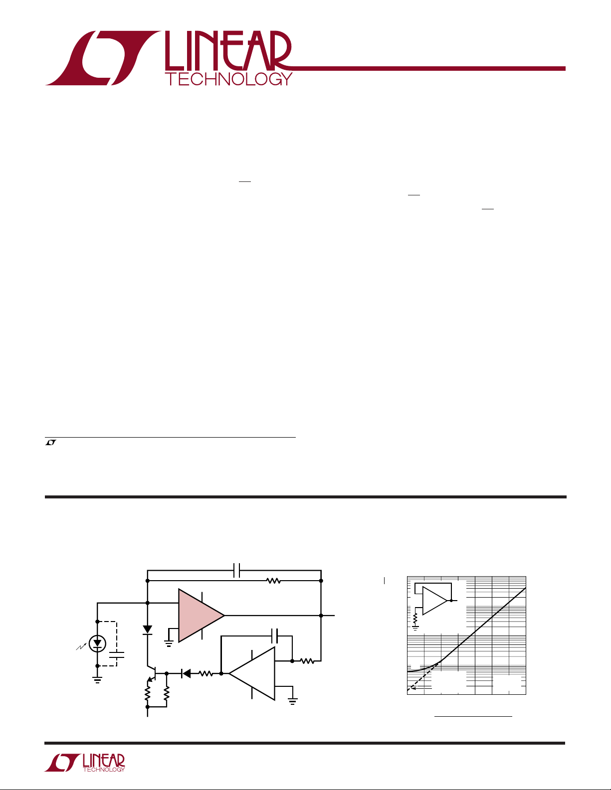
TYPICAL APPLICATIO
Low Noise Light Sensor with DC Servo
–
2
LT1793
+
3
D1
1N914
R5
R4
10k
1k
R2C2 > C1R1
C
–
V
D
V
OUT
330mV/µWATT FOR 633nm WAVE LENGTH
HAMAMATSU
S1336-5BK
(908) 231-0960
1N914
C
D
2N3904
D2
U
C1
2pF
+
V
7
6
4
–
V
R3
1k
= PARASITIC PHOTODIODE CAPACITANCE
= 100mV/µWATT FOR 200nm WAVE LENGTH
C2 0.022µF
+
V
LT1097
–
V
R1
1M
–
+
R2
100k
1793 TA01
1kHz Output Voltage Noise
Density vs Source Resistance
10k
–
1k
10
1
100 10k 100k 1M1k
R
SOURCE
V
N
VN = √(V
+
V
OUT
100
TOTAL 1kHz VOLTAGE NOISE DENSITY (nV/√Hz)
V
N
SOURCE
RESISTANCE
ONLY
SOURCE RESISTANCE (Ω)
OP AMP
10M
)2 + 4kTRS + 2qIBR
TA = 25°C
= ±15V
V
S
100M
2
S
1793 TA02
1G
1
Page 2
LT1793
A
W
O
LUTEXI TIS
S
A
WUW
U
ARB
G
(Note 1)
Supply Voltage ..................................................... ±20V
Differential Input Voltage ...................................... ±40V
Input Voltage (Equal to Supply Voltage)............... ±20V
Output Short-Circuit Duration ........................ Indefinite
Operating Temperature Range............... –40°C to 85°C
WU
/
PACKAGE
VOS ADJ
–IN A
+IN A
–
V
T
JMAX
Consult factory for Military grade parts.
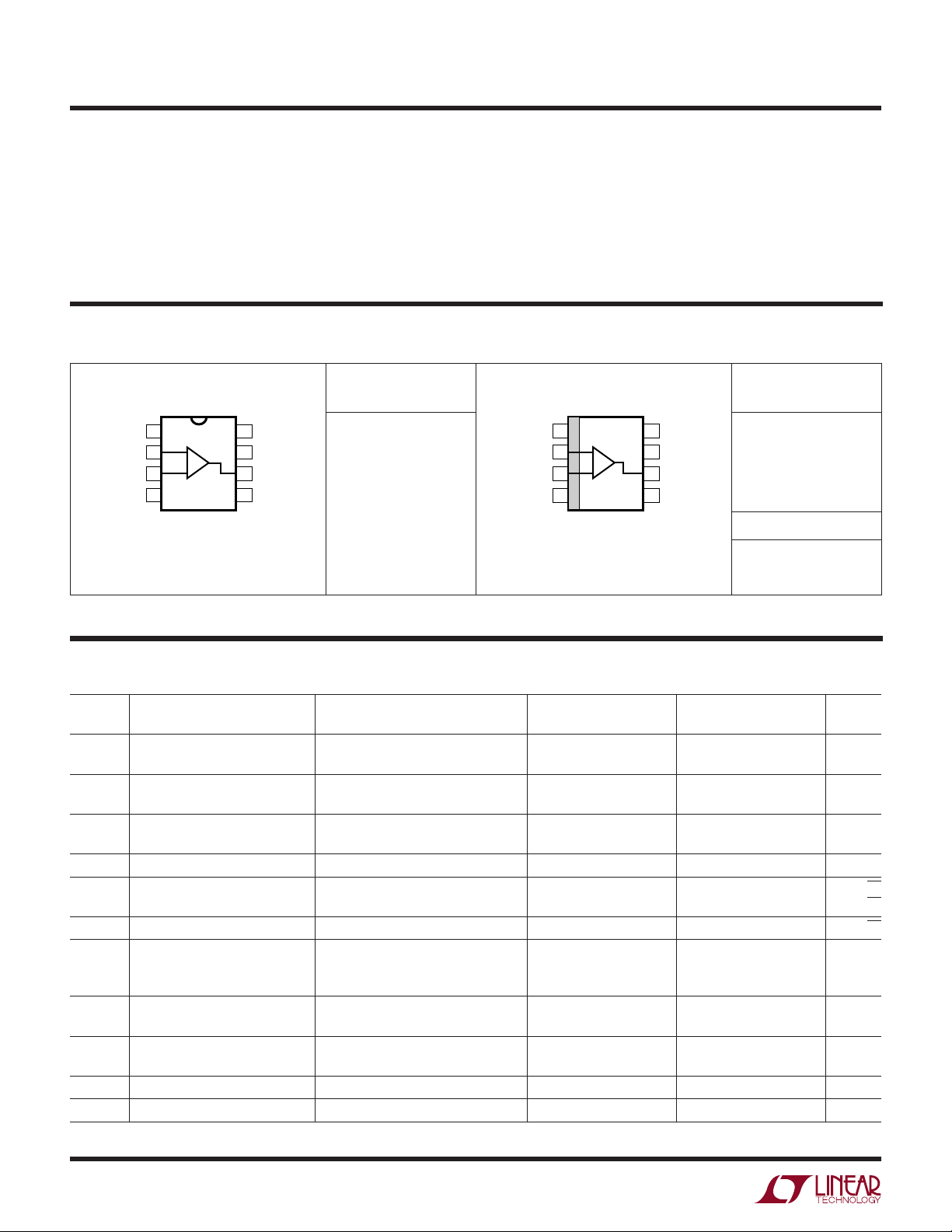
O
RDER I FOR ATIO
TOP VIEW
1
2
A
3
4
N8 PACKAGE
8-LEAD PDIP
= 150°C, θJA = 80°C/W
ORDER PART
NUMBER
NC
8
+
V
7
OUT
6
ADJ
V
5
OS
LT1793ACN8
LT1793CN8
LT1793AIN8
LT1793IN8
Specified Temperature Range
Commercial (Note 8) ......................... –40°C to 85°C
Industrial ........................................... –40°C to 85°C
Storage Temperature Range................ –65°C to 150°C
Lead Temperature (Soldering, 10 sec) ................ 300°C
U
ORDER PART
NUMBER
LT1793ACS8
LT1793CS8
LT1793AIS8
LT1793IS8
S8 PART MARKING
1793A
1793
VOS ADJ
–IN A
+IN A
TOP VIEW
1
2
A
3
–
V
4
S8 PACKAGE
8-LEAD PLASTIC SO
T
= 160°C, θJA = 190°C/W
JMAX
NC
8
V+
7
OUT
6
ADJ
V
5
OS
1793AI
1793I
T
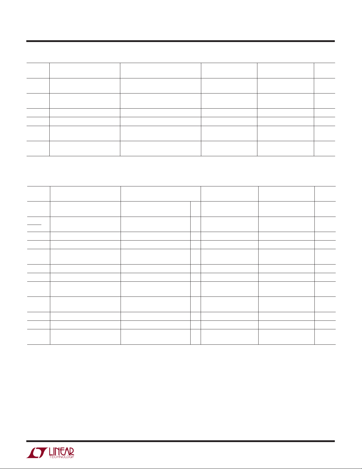
LECTRICAL C CHARA TERIST
E
SYMBOL PARAMETER CONDITIONS (Note 2) MIN TYP MAX MIN TYP MAX UNITS
V
OS
I
OS
I
B
e
n
i
n
R
IN
C
IN
V
CM
CMRR Common Mode Rejection Ratio V
PSRR Power Supply Rejection Ratio VS = ±4.5V to ± 20V 85 98 83 95 dB
Input Offset Voltage 0.25 0.8 0.25 0.9 mV
V
S
Input Offset Current Warmed Up (Note 3) 1.5 7 2.5 15 pA
T
J
Input Bias Current Warmed Up (Note 3) 3 10 4.0 20 pA
T
J
Input Noise Voltage 0.1Hz to 10Hz 2.4 2.4 µV
Input Noise Voltage Density fO = 10Hz 11.5 11.5 nV/√Hz
f
O
Input Noise Current Density fO = 10Hz, fO = 1kHz (Note 4) 0.8 1 fA/√Hz
Input Resistance
Differential Mode 10
Common Mode V
Input Capacitance 1.5 1.5 pF
Input Voltage Range (Note 5) 13.0 13.5 13.0 13.5 V
CM
V
S
CM
ICS
= ±5V 0.45 1.4 0.45 1.6 mV
= 25°C (Note 6) 0.5 2 0.7 4 pA
= 25°C (Note 6) 1 3 1.5 5 pA
= 1000Hz 6 8 6 8 nV/√Hz
= –10V to 13V 10
= ±5V 2.0 2.0 pF
= –10V to 13V 83 102 81 96 dB
= 25°C, VS = ±15V, V
A
= 0V, unless otherwise noted.
CM
LT1793AC/LT1793AI
14
13
–10.5 –11.0 – 10.5 – 11.0 V
LT1793C/LT1793I
14
10
13
10
P-P
Ω
Ω
2
Page 3
LT1793
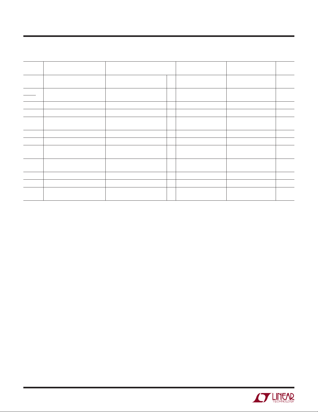
T
LECTRICAL C CHARA TERIST
E
SYMBOL PARAMETER CONDITIONS (Note 2) MIN TYP MAX MIN TYP MAX UNITS
A
VOL
V
OUT
SR Slew Rate RL ≥ 2k (Note 7) 2.3 3.4 2.3 3.4 V/µs
GBW Gain-Bandwidth Product fO = 100kHz 2.5 4.2 2.5 4.2 MHz
I
S
Large-Signal Voltage Gain VO = ±12V, RL = 10k 1000 4500 900 4400 V/mV
V
O
Output Voltage Swing RL = 10k ±13.0 ±13.2 ±13.0 ±13.2 V
R
L
Supply Current 4.2 5.20 4.2 5.20 mA
V
S
Offset Voltage R
Adjustment Range
POT
ICS
= ±10V, RL = 1k 500 3500 400 3000 V/mV
= 1k ±12.0 ±12.3 ±12.0 ±12.3 V
= ±5V 4.2 5.15 4.2 5.15 mA
(to VEE) = 10k 13 13 mV
= 25°C, VS = ±15V, V
A
The ● denotes specifications which apply over the temperature range 0°C ≤ TA ≤ 70°C, otherwise specifications are at TA = 25°C.
V
= ±15V, V
S
SYMBOL PARAMETER CONDITIONS (Note 2) MIN TYP MAX MIN TYP MAX UNITS
V
OS
∆V
OS
∆Temp Voltage Drift
I
OS
I
B
V
CM
CMRR Common Mode Rejection Ratio V
PSRR Power Supply Rejection Ratio VS = ±4.5V to ± 20V ● 83 97 81 94 dB
A
VOL
V
OUT
SR Slew Rate RL ≥ 2k (Note 7) ● 2.2 3.3 2.2 3.3 V/µs
GBW Gain-Bandwidth Product fO = 100kHz ● 2.2 3.3 2.2 3.3 MHz
I
S
= 0V, unless otherwise noted. (Note 9)
CM
Input Offset Voltage ● 0.50 1.0 1.0 3.5 mV
= ±5V ● 0.75 1.6 1.6 4.2 mV
V
S
Average Input Offset (Note 6) ● 513 850 µV/°C
Input Offset Current ● 15 100 20 130 pA
Input Bias Current ● 130 400 150 500 pA
Input Voltage Range (Note 5) ● 12.9 13.4 12.9 13.4 V
● – 10.0 –10.8 – 10.0 – 10.8 V
= –10V to 12.9V ● 79 100 77 95 dB
CM
Large-Signal Voltage Gain VO = ±12V, RL = 10k ● 900 3600 800 3400 V/mV
= ±10V, RL = 1k ● 500 2600 400 2400 V/mV
V
O
Output Voltage Swing RL = 10k ● ±12.9 ±13.2 ±12.9 ±13.2 V
R
= 1k ● ±11.9 ±12.15 ±11.9 ±12.15 V
L
Supply Current ● 4.2 5.30 4.2 5.30 mA
V
= ±5V ● 4.2 5.25 4.2 5.25 mA
S
= 0V, unless otherwise noted.
CM
LT1793AC/LT1793AI
LT1793AC LT1793C
LT1793C/LT1793I
3
Page 4
LT1793
LECTRICAL C CHARA TERIST
E
–40°C ≤ TA ≤ 85°C. VS = ±15V, V
SYMBOL PARAMETER CONDITIONS (Note 2) MIN TYP MAX MIN TYP MAX UNITS
V
OS
∆V
∆Temp Voltage Drift
I
OS
I
B
V
CM
CMRR Common Mode Rejection Ratio V
PSRR Power Supply Rejection Ratio VS = ±4.5V to ± 20V ● 81 96 79 93 dB
A
VOL
V
OUT
SR Slew Rate RL ≥ 2k ● 2.1 3.2 2.1 3.2 V/µs
GBW Gain-Bandwidth Product fO = 100kHz ● 23.1 23.1 MHz
I
S
OS
Input Offset Voltage ● 0.65 1.3 1.6 4.8 mV
Average Input Offset (Note 6) ● 513 950 µV/°C
Input Offset Current ● 80 300 100 400 pA
Input Bias Current ● 700 2400 800 3000 pA
Input Voltage Range (Note 5) ● 12.6 13.0 12.6 13.0 V
Large-Signal Voltage Gain VO = ±12V, RL = 10k ● 850 3300 750 3000 V/mV
Output Voltage Swing RL = 10k ● ±12.8 ±13.1 ±12.8 ±13.1 V
Supply Current ● 4.2 5.40 4.2 5.40 mA
= 0V, unless otherwise noted. (Notes 8, 9)
CM
V
S
CM
V
O
R
L
V
S
ICS
= ±5V ● 1.00 1.9 2.0 5.5 mV
= –10V to 12.6V ● 78 99 76 94 dB
= ±10V, RL = 1k ● 400 2200 300 2000 V/mV
= 1k ● ±11.8 ±12.1 ±11.8 ±12.1 V
= ±5V ● 4.2 5.35 4.2 5.35 mA
The ● denotes specifications which apply over the temperature range
LT1793AC/LT1793AI LT1793C/LT1793I
● – 10.0 –10.5 – 10.0 – 10.5 V
Note 1: Absolute Maximum Ratings are those values beyond which the life
of a device may be impaired.
Note 2: Typical parameters are defined as the 60% yield of parameter
distributions of individual amplifiers.
Note 3: I
from 25°C measurements and 32°C characterization data.
Note 4: Current noise is calculated from the formula:
where q = 1.6 • 10
swamps the contribution of current noise.
Note 5: Input voltage range functionality is assured by testing offset
voltage at the input voltage range limits to a maximum of 2.3mV
(A grade) to 2.8mV (C grade).
and IOS readings are extrapolated to a warmed-up temperature
B
1/2
= (2qIB)
i
n
–19
coulomb. The noise of source resistors up to 200M
Note 6: This parameter is not 100% tested.
Note 7: Slew rate is measured in A
measured at ±2.5V.
Note 8: The LT1793AC and LT1793C are guaranteed to meet specified
performance from 0°C to 70°C and are designed, characterized and
expected to meet these extended temperature limits, but are not tested at
–40°C and 85°C. The LT1793I is guaranteed to meet the extended
temperature limits. The LT1793AC and LT1793AI grade are 100%
temperature tested for the specified temperature range.
Note 9: The LT1793 is measured in an automated tester in less than one
second after application of power. Depending on the package used, power
dissipation, heat sinking, and air flow conditions, the fully warmed-up chip
temperature can be 10°C to 50°C higher than the ambient temperature.
= –1; input signal is ±7.5V, output
V
4
Page 5

LPER
F
0.1Hz to 10Hz Voltage Noise
VOLTAGE NOISE (1µV/DIV)
2468
TIME (SEC)
O
R
ATYPICA
100
1793 G01
UW
CCHARA TERIST
E
C
1kHz Input Noise Voltage
Distribution
50
TA = 25°C
= ±15V
V
S
510 OP AMPS TESTED
40
30
20
PERCENT OF UNITS (%)
10
0
5.0
4.2
4.6 7.8
INPUT VOLTAGE NOISE (nV/√Hz)
5.4
5.8
6.2
6.6
ICS
7.0
7.4
1793 G02
8.2
Voltage Noise vs Frequency
100
TA = 25°C
V
= ±15V
S
10
1/f CORNER
30Hz
RMS VOLTAGE NOISE DENSITY (nV/√Hz)
1
110
100 1k 10k
FREQUENCY (Hz)
LT1793
1793 G03
Voltage Noise
vs Chip Temperature
10
VS = ±15V
9
8
7
6
5
4
VOLTAGE NOISE (AT 1kHz) (nV/√Hz)
3
2
–75
–50 –25
0
TEMPERATURE (°C)
50
25
Power Supply Rejection Ratio
vs Frequency
120
100
+PSRR
80
60
40
20
POWER SUPPLY REJECTION RATIO (dB)
0
–PSRR
10
1k 10k 100k
100
FREQUENCY (Hz)
75
100
TA = 25°C
1M 10M
1793 G04
1793 G07
+
V
–0.5
–1.0
–1.5
–2.0
3.5
COMMON MODE LIMIT (V)
3.0
REFERRED TO POWER SUPPLY
2.5
–
+2.0
V
125
180
160
140
120
100
80
60
VOLTAGE GAIN (dB)
40
20
0
–20
0.01
Common Mode Limit
vs Temperature
0
V+ = 5V TO 20V
4.0
–
= –5V TO –20V
V
–60
–20
TEMPERATURE (°C)
60
20
Voltage Gain vs Frequency
TA = 25°C
= ±15V
V
S
C
= 10pF
L
1
FREQUENCY (Hz)
100
10k
1M
100
100M
1793 G08
140
1793 G05
Common Mode Rejection Ratio
vs Frequency
120
100
80
60
40
20
COMMON MODE REJECTION RATIO (dB)
0
1k 100k 1M 10M
10k
FREQUENCY (Hz)
Gain and Phase Shift
vs Frequency
50
40
30
20
10
VOLTAGE GAIN (dB)
0
–10
0.1
GAIN
1 10 100
FREQUENCY (MHz)
PHASE
TA = 25°C
= ±15V
V
S
= 10pF
C
L
1793 G09
TA = 25°C
V
= ±15V
S
1793 G06
80
100
120
140
160
180
200
PHASE SHIFT (DEG)
5
Page 6

LT1793
LPER
Small-Signal Transient Response
20mV/DIV
AV = 1
= 10pF
C
L
= ±15V, ±5V
V
S
Capacitive Load Handling
50
VS = ±15V
= 25°C
T
A
≥ 10k
R
L
40
= 100mV
V
O
AV = 10
= 10k
R
F
30
= 20pF
C
F
20
OVERSHOOT (%)
10
0
0.1
1µs/DIV
P-P
A
= 1
V
= 10
A
V
1
10
CAPACITIVE LOAD (pF)
R
F
O
100
1793 G10
1000
ATYPICA
10000
1793 G13
UW
CCHARA TERIST
E
C
Large-Signal Transient Response
5V/DIV
AV = 1
= 10pF
C
L
= 2k
R
L
V
= ±15V
S
Warm-Up Drift
90
VS = ±15V
= 25°C
T
A
75
60
45
30
15
CHANGE IN OFFSET VOLTAGE (µV)
0
0
1
TIME AFTER POWER ON (MINUTES)
ICS
5µs/DIV
SO-8 PACKAGE
N8 PACKAGE
234
1793 G11
56
1793 G14
Output Voltage Swing
vs Load Current
V+ –0.8
–1.0
–1.2
–1.4
–1.6
2.0
1.8
1.6
1.4
OUTPUT VOLTAGE SWING (V)
1.2
–
V
+1.0
–8
–10
I
SINK
25°C
–55°C
VS = ±5V TO ±20V
125°C
–55°C
–6 –4
OUTPUT CURRENT (mA)
25°C
048
–2
2
THD and Noise Frequency for
Noninverting Gain
1
ZL = 2k 15pF
= 20V
V
O
P-P
= 1, 10, 100
A
V
MEASUREMENT BANDWIDTH
0.1
= 10Hz TO 80kHz
AV = 10
AV = 100
AV = 1
NOISE FLOOR
1k 20k10k
FREQUENCY (Hz)
0.01
0.001
TOTAL HARMONIC DISTORTION + NOISE (%)
0.0001
20 100
125°C
6
I
SOURCE
1793 G12
1793 G15
10
THD and Noise vs Frequency for
Inverting Gain
1
ZL = 2k 15pF
= 20V
V
O
P-P
= –1, –10, – 100
A
V
MEASUREMENT BANDWIDTH
0.1
= 10Hz TO 80kHz
0.01
0.001
TOTAL HARMONIC DISTORTION + NOISE (%)
0.0001
20 100
FREQUENCY (Hz)
AV = –100
AV = –10
NOISE FLOOR
1k 20k10k
6
AV = –1
1793 G16
THD and Noise vs Output
Amplitude for Inverting Gain
1
ZL = 2k 15pF, fO = 1kHz
A
= –1, –10, –100
V
MEASUREMENT BANDWIDTH
= 10Hz TO 22kHz
0.1
0.01
0.001
TOTAL HARMONIC DISTORTION + NOISE (%)
0.0001
0.3
AV = –100
AV = –10
AV = –1
11030
OUTPUT SWING (V
P-P
THD and Noise vs Output
Amplitude for Noninverting Gain
1
ZL = 2k 15pF, fO = 1kHz
A
= 1, 10, 100
V
MEASUREMENT BANDWIDTH
= 10Hz TO 22kHz
0.1
0.01
0.001
TOTAL HARMONIC DISTORTION + NOISE (%)
0.0001
)
1793 G17
0.3
AV = 100
AV = 10
AV = 1
11030
OUTPUT SWING (V
P-P
)
1793 G18
Page 7

LPER
TEMPERATURE (°C)
0
INPUT BIAS AND OFFSET CURRENTS (A)
300p
100p
3n
1n
30n
10n
100
1793 G21
30p
10p
3p
1p
0.3p
25
50
75
125
VS = ±15V
V
CM
= –10 TO 13V
BIAS
CURRENT
OFFSET
CURRENT
2
3
1
5
∆V
OS
= ±13mV
50k
15V
–15V
4
6
7
–
+
2
3
1
5
∆V
OS
= ±1.3mV
50k
10k
10k
15V
–15V
(b)(a)
1793 F02
4
6
7
–
+
F
O
R
ATYPICA
UW
CCHARA TERIST
E
C
LT1793
ICS
Short-Circuit Output Current
vs Temperature
40
V
= ±15V
S
35
30
SINK SOURCE
25
20
OUTPUT CURRENT (mA)
15
10
–75
–50 0
–25 5025
TEMPERATURE (°C)
PPLICATI
A
LT1793 vs the Competition
With improved noise performance, the LT1793 in the
PDIP directly replaces such JFET op amps as the OPA111
and the AD645. The combination of low current and
voltage noise of the LT1793 allows it to surpass most dual
and single JFET op amps. The LT1793 can replace many
of the lowest noise bipolar amps that are used in amplifying low level signals from high impedance transducers.
The best bipolar op amps (with higher current noise) will
eventually lose out to the LT1793 when transducer impedance increases.
100
CURRENT NOISE = √2qI
80
60
40
20
0
–20
–40
INPUT BIAS CURRENT (pA)
–60
–80
–100
–15
Figure 1. Comparison of LT1793, OP215, and AD822
Input Bias Current vs Common Mode Range
75
100
U
O
I FOR ATIO
S
B
AD822
–10
–5
COMMON MODE RANGE (V)
05
1793 G19
OP215
5
4
SUPPLY CURRENT PER AMPLIFIER (mA)
125
3
–75
WU
LT1793
10
15
1793 F01
Supply Current vs Temperature
VS = ±15V
VS = ±5V
75
–50 0
–25 5025
TEMPERATURE (°C)
100
U
The extremely high input impedance (1013Ω) assures that
the input bias current is almost constant over the entire
common mode range. Figure 1 shows how the LT1793
stands up to the competition. Unlike the competition, as the
input voltage is swept across the entire common mode
range the input bias current of the LT1793 hardly changes.
As a result the current noise does not degrade. This makes
the LT1793 the best choice in applications where an
amplifier has to buffer signals from a high impedance
transducer.
Offset nulling will be compatible with these devices with the
wiper of the potentiometer tied to the negative supply
(Figure 2a). No appreciable change in offset voltage drift
Input Bias and Offset Currents
vs Chip Temperature
125
1793 G20
Figure 2
7
Page 8

LT1793
PPLICATI
A
U
O
I FOR ATIO
S
WU
U
with temperature will occur when the device is nulled with
a potentiometer ranging from 10k to 200k. Finer adjustments can be made with resistors in series with the
potentiometer (Figure 2b).
Amplifying Signals from High Impedance Transducers
The low voltage and current noise offered by the LT1793
makes it useful in a wide range of applications, especially
where high impedance, capacitive transducers are used
such as hydrophones, precision accelerometers and
photodiodes. The total output noise in such a system is
the gain times the RMS sum of the op amp’s input referred
10k
C
S
–
1k
100
10
INPUT NOISE VOLTAGE (nV/√Hz)
1
100
R
+
R
C
S
LT1793
RESISTOR NOISE ONLY
1k 100M 1G
SOURCE RESISTANCE = 2RS = R
* PLUS RESISTOR
†
PLUS RESISTOR 1000pF CAPACITOR
Vn = AV √V
Figure 3. Comparison of LT1793 and LT1007 Total Output
1kHz Voltage Noise vs Source Resistance
LT1007*
LT1793*
S
V
O
S
LT1007
†
LT1793
LT1007
100k
SOURCE RESISTANCE (Ω)
n2(OP AMP)
10M10k 1M
+ 4kTR + 2qIBR
†
1793 F03
2
voltage noise, the thermal noise of the transducer, and the
op amp’s input bias current noise times the transducer
impedance.
Figure 3 shows total input voltage noise
versus source resistance. In a low source resistance
(< 5k) application the op amp voltage noise will dominate
the total noise. This means the LT1793 is superior to
most JFET op amps. Only the lowest noise bipolar op
amps have the advantage at low source resistances. As
the source resistance increases from 5k to 50k, the
LT1793 will match the best bipolar op amps for noise
perfor
mance, since the thermal noise of the transducer
(4kTR) begins to dominate the total noise. A further
increase in source resistance, above 50k, is where the op
amp’s current noise component (2qIBR2) will eventually
dominate the total noise. At these high source resistances, the LT1793 will out perform the lowest noise
bipolar op amps due to the inherently low current noise of
FET input op amps. Clearly, the LT1793 will extend the
range of high impedance transducers that can be used for
high signal-to-noise ratios. This makes the LT1793 the
best choice for high impedance, capacitive transducers.
Optimization Techniques for Charge Amplifiers
The high input impedance JFET front end makes the
LT1793 suitable in applications where very high charge
sensitivity is required. Figure 4 illustrates the LT1793 in its
inverting and noninverting modes of operation. A charge
amplifier is shown in the inverting mode example; the gain
depends on the principal of charge conservation at the
input of the LT1793. The charge across the transducer
capacitance CS is transferred to the feedback capacitor C
F
8
C
S
TRANSDUCER
R
F
C
F
–
R
S
C
B
+
R
B
CB = CFC
RB = RFR
Q = CV; = I = C
OUTPUT
S
S
dQ
dV
dt
dt
R1
C
S
TRANSDUCER
Figure 4. Inverting and Noninverting Gain Configurations
R2
C
B
R
B
–
OUTPUT
+
R
S
CB ≅ C
S
RB = R
S
RS > R1 OR R2
1793 F04
Page 9

LT1793
U
O
PPLICATI
A
resulting in a change in voltage dV, which is equal to dQ/CF.
The gain therefore is CF/CS. For unity-gain, the CF should
equal the transducer capacitance plus the input capacitance of the LT1793 and RF should equal RS.
In the noninverting mode example, the transducer current
is converted to a change in voltage by the transducer
capacitance, CS. This voltage is then buffered by the
LT1793 with a gain of 1 + R1/R2. A DC path is provided by
RS, which is either the transducer impedance or an external resistor. Since RS is usually several orders of magnitude greater than the parallel combination of R1 and R2, R
is added to balance the DC offset caused by the noninverting input bias current and RS. The input bias currents,
although small at room temperature, can create significant
errors at higher temperature, especially with transducer
resistances of up to 1000M or more. The optimum value
Input: ±5.2V Sine Wave
I FOR ATIO
S
WU
U
B
for RB is determined by equating the thermal noise (4kTRS)
to the current noise (2qIB) times R
results in RB = RS = 2VT/IB (VT = 26mV at 25°C). A parallel
capacitor CB, is used to cancel the phase shift caused by
the op amp input capacitance and RB.
Reduced Power Supply Operation
To take full advantage of a wide input common mode range,
the LT1793 was designed to eliminate phase reversal.
Referring to the photographs in Figure 5, the LT1793 is
shown operating in the follower mode (AV = 1) at ±5V
supplies with the input swinging ±5.2V. The output of the
LT1793 clips cleanly and recovers with no phase reversal.
This has the benefit of preventing lockup in servo systems
and minimizing distortion components.
LT1793 Output
2
. Solving for R
S
S
LT1793 F05a LT1793 F05b
Figure 5. Voltage Follower with Input Exceeding the Common Mode Range (V
= ±5V)
S
9
Page 10

LT1793
PACKAGEDESCRIPTI
O
U
Dimensions in inches (millimeters) unless otherwise noted.
N8 Package
8-Lead PDIP (Narrow 0.300)
(LTC DWG # 05-08-1510)
0.400*
(10.160)
MAX
876
0.255 ± 0.015*
(6.477 ± 0.381)
5
12
0.300 – 0.325
(7.620 – 8.255)
0.065
(1.651)
0.009 – 0.015
(0.229 – 0.381)
+0.035
0.325
–0.015
+0.889
8.255
()
–0.381
*THESE DIMENSIONS DO NOT INCLUDE MOLD FLASH OR PROTRUSIONS.
MOLD FLASH OR PROTRUSIONS SHALL NOT EXCEED 0.010 INCH (0.254mm)
TYP
(2.540 ± 0.254)
0.045 – 0.065
(1.143 – 1.651)
0.100 ± 0.010
3
4
0.130 ± 0.005
(3.302 ± 0.127)
0.125
(3.175)
MIN
0.018 ± 0.003
(0.457 ± 0.076)
0.020
(0.508)
MIN
N8 1197
10
Page 11

PACKAGEDESCRIPTI
U
O
Dimensions in inches (millimeters) unless otherwise noted.
S8 Package
8-Lead Plastic Small Outline (Narrow 0.150)
(LTC DWG # 05-08-1610)
8
0.189 – 0.197*
(4.801 – 5.004)
7
6
LT1793
5
0.228 – 0.244
(5.791 – 6.197)
0.010 – 0.020
(0.254 – 0.508)
0.008 – 0.010
(0.203 – 0.254)
*
DIMENSION DOES NOT INCLUDE MOLD FLASH. MOLD FLASH
SHALL NOT EXCEED 0.006" (0.152mm) PER SIDE
**
DIMENSION DOES NOT INCLUDE INTERLEAD FLASH. INTERLEAD
FLASH SHALL NOT EXCEED 0.010" (0.254mm) PER SIDE
×
°
45
0.016 – 0.050
0.406 – 1.270
0°– 8° TYP
0.053 – 0.069
(1.346 – 1.752)
0.014 – 0.019
(0.355 – 0.483)
0.150 – 0.157**
(3.810 – 3.988)
1
3
2
4
0.004 – 0.010
(0.101 – 0.254)
0.050
(1.270)
TYP
SO8 0996
Information furnished by Linear Technology Corporation is believed to be accurate and reliable.
However, no responsibility is assumed for its use. Linear Technology Corporation makes no representation that the interconnection of its circuits as described herein will not infringe on existing patent rights.
11
Page 12

LT1793
g
U
TYPICAL APPLICATIONS N
10Hz Fourth Order Chebyshev Lowpass Filter (0.01dB Ripple)
R2
237k
R5
154k
R3
R1
249k
237k
V
IN
C2
100nF
TYPICAL OFFSET ≈ 0.8mV
1% TOLERANCES
= 10V
FOR V
IN
= – 6dB AT f = 16.3Hz
LOWER RESISTOR VALUES WILL RESULT IN LOWER THERMAL NOISE AND LARGER CAPACITORS
P-P
, V
OUT
15V
C1
LT1793
–15V
33nF
7
6
4
–
2
+
3
= –121dB AT f > 330Hz
R4
154k
R6
249k
C4
330nF
C3
10nF
–
2
LT1793
+
3
6
Accelerometer Amplifier with DC Servo
C1
1250pF
ACCELEROMETER
B & K MODEL 4381
OR EQUIVALENT
(800) 442-1030
R1
100M
5V TO 15V
–
2
LT1793
+
3
–5V TO –15V
R3
2k
1
7
4
2µF
1/2 LT1464
6
R2
18k
C2
R4
20M
–
2
R5
20M
+
3
C3
2µF
1793 TA03
R4C2 = R5C3 > R1 (1 + R2/R3) C1
OUTPUT = 0.8mV/pC* = 8.0mV/g**
DC OUTPUT ≤ 1.9mV
OUTPUT NOISE = 8nV/√Hz AT 1kHz
*PICOCOULOMBS
= EARTH’S GRAVITATIONAL CONSTANT
**
OUTPUT
V
OUT
1793 TA04
RELATED PARTS
PART NUMBER DESCRIPTION COMMENTS
LT1113 Low Noise, Dual JFET Op Amp Dual Version of LT1792, V
LT1169 Low Noise, Dual JFET Op Amp Dual Version of LT1793, V
LT1467 Micropower Dual JFET Op Amp 1MHz, 2pA Max IB, 200µA Max I
LT1792 Low Noise, Single JFET Op Amp Lower V
Version of LT1793, V
NOISE
Linear Technology Corporation
12
1630 McCarthy Blvd., Milpitas, CA 95035-7417
(408) 432-1900 ● FAX: (408) 434-0507
●
www.linear-tech.com
NOISE
NOISE
= 4.5nV/√Hz
= 6nV/√Hz, IB = 10pA
S
= 4.2nV/√Hz
NOISE
1793f LT/TP 0599 4K • PRINTED IN USA
LINEAR TECHNOLOGY CORPORATION 1999
 Loading...