

Page 1
LT1786F
SMBus Programmable
CCFL Switching Regulator
FEATURES
■
Wide Battery Input Range: 4.5V to 30V
■
Grounded Lamp or Floating Lamp Configurations
■
Open Lamp Protection
■
Precision 100µA Full-Scale DAC
Programming Current
■
2-Wire SMBus Interface
■
Two Selectable SMBus Addresses
■
DAC Setting Is Retained in Shutdown
U
APPLICATIONS
■
Notebook and Palmtop Computers
■
Portable Instruments
■
Personal Digital Assistants
U
DESCRIPTION
The LT®1786F is a fixed frequency, current mode, switching regulator that provides the control function for Cold
Cathode Fluorescent Lighting (CCFL). The IC includes an
efficient high current switch, an oscillator, output drive
logic, control circuitry and a micropower 6-bit 100µ A fullscale current output DAC. The DAC provides simple “bits-
to-lamp-current control” and communicates using the
2-wire SMBus serial interface. The LT1786F acts as an
SMBus slave device using one of two selectable SMBus
addresses set by the address pin ADR.
On Power-up, the DAC output current assumes midrange
or zero scale, depending on the logic state of the ADR
pin.The entire IC can be shut down through the SMBSUS
pin or by setting the SHDN bit = 1 in the SMBus command
byte. Digital data for the DAC output current is retained
internally and the supply current drops to 40µ A for standby
operation. The active low SHDN pin disables the CCFL
control circuitry, but keeps the DAC alive. Supply current
in this operating mode drops to 150µA.
The LT1786F control circuitry operates from a logic supply
voltage of 3.3V or 5V. The IC also has a battery supply pin
that operates from 4.5V to 30V. The LT1786F draws 6mA
typical quiescent current. A 200kHz switching frequency
minimizes magnetic component size. Current mode switching techniques with cycle-by-cycle limiting gives high
reliability and simple loop frequency compensation. The
LT1786F is available in a 16-pin narrow SO package.
, LTC and LT are registered trademarks of Linear Technology Corporation.
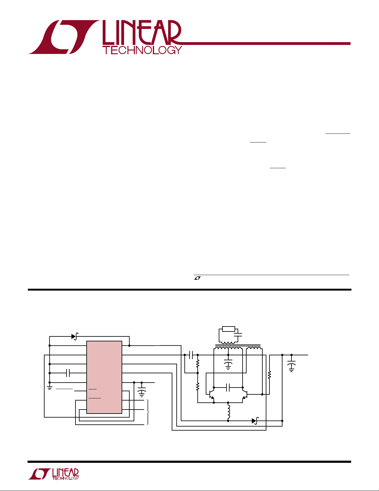
TYPICAL APPLICATION
90% Efficient Floating CCFL with 2-Wire SMBus Control of Lamp Current
D1
BAT85
1
CCFL
PGND
2
I
CCFL
3
C7, 1µF
SHUTDOWN
ALUMINUM ELECTROLYTIC IS RECOMMENDED FOR C3A AND C3B.
MAKE 3CB ESR ≥ 0.5Ω TO PREVENT DAMAGE TO THE LT1786F HIGH-SIDE
SENSE RESISTOR DUE TO SURGE CURRENTS AT TURN-ON
C1 MUST BE A LOW LOSS CAPACITOR, C1 = WIMA MKI OR MKP-20
= PANASONIC ECH-U
Q1, Q2 = ZETEX ZTX849 OR ROHM 2SC5001
4
5
6
7
8
DIO
CCFL V
AGND
SHDN
SMBSUS
ADR
LT1786F
C
CCFL V
ROYER
BULB
BAT
V
I
OUT
SCL
SDA
16
SW
15
14
13
12
CC
11
10
9
U
CCFL BACKLIGHT APPLICATION CIRCUITS
CONTAINED IN THIS DATA SHEET ARE COVERED
BY U.S. PATENT NUMBER 5408162
AND OTHER PATENTS PENDING
3V ≤ V
CC
≤ 6.5V
+
C4
2.2µF
TO
SMBus
HOST
0µA TO 50µA I
0mA TO 6mA LAMP CURRENT
FOR A TYPICAL DISPLAY.
C5
1000pF
R3
100k
CCFL
LAMP
10
321 5
R2
220k
CURRENT GIVES
+
C1*
0.068µF
Q2* Q1*
L1 = COILTRONICS CTX210605
L2 = COILTRONICS CTX100-4
*DO NOT SUBSTITUTE COMPONENTS
COILTRONICS (561) 241-7876
L1
+
C3A
2.2µF
R1
750Ω
35V
BAT
8V TO 28V
6
C3B
2.2µF
35V
C2
27pF
3kV
4
L2
100µH
FOR ADDITIONAL CCFL/LCD CONTRAST APPLICATION CIRCUITS,
REFER TO THE LT1182/83/84/84F DATA SHEET
D1
1N5818
1786F TA01
1
Page 2
LT1786F
WW
W
U
ABSOLUTE MAXIMUM RATINGS
VCC........................................................................... 7V
BAT, Royer, BULB .................................................. 30V
CCFL VSW............................................................... 60V
Shutdown ................................................................. 6V
I
Input Current .............................................. 10mA
CCFL
DIO Input Current (Peak, <100ms).................... 100mA
Digital Inputs .............................. –0.3V to (VCC + 0.3V)
Digital Outputs............................ –0.3V to (VCC + 0.3V)
DAC Output Voltage ..................... –15V to (VCC + 0.3V)
Junction Temperature (Note 1)............................ 100°C
Operating Ambient Temperature Range ..... 0°C to 70°C
Storage Temperature Range ................ –65°C to 150°C
Lead Temperature (Soldering, 10 sec)................. 300°C
U
PACKAGE/ORDER INFORMATION
TOP VIEW
16
CCFL V
SW
15
BULB
14
BAT
13
ROYER
12
V
CC
11
I
OUT
10
SCL
9
SDA
I
CCFL
CCFL V
AGND
SHDN
ADR
1
2
3
DIO
4
C
5
6
7
8
S PACKAGE
16-LEAD PLASTIC SO
T
= 100°C, θJA = 100°C/W
JMAX
CCFL PGND
SMBSUS
Consult factory for Industrial and Military grade parts.
W
ORDER PART
NUMBER
LT1786FCS
ELECTRICAL CHARACTERISTICS
TA = 25°C, VCC = SHUTDOWN = SMBSUS = SCL = SDA = 3.3V, BAT = Royer = BULB = 12V, I
DIO = I
SYMBOL PARAMETER CONDITIONS MIN TYP MAX UNITS
I
Q
ISUS SMBSUS Supply Current SMBSUS = 0V or Command Code Bit 7 = 1, ● 40 100 µA
I
SHDN
f Switching Frequency Measured at CCFL VSW, ISW = 50mA, 175 200 225 kHz
DC(MAX) Maximum Switch Duty Cycle Measured at CCFL V
BV Switch Breakdown Voltage Measured at CCFL V
= GND, CCFL VC = 0.5V, unless otherwise specified.
OUT
Supply Current 3V ≤ VCC ≤ 6.5V, I
CCFL VC = Open (Note 2)
SHUTDOWN Supply Current SHUTDOWN = 0V, CCFL VC = Open (Note 2) ● 150 300 µA
SHUTDOWN Input Bias Current SHUTDOWN = 0V, CCFL VC = Open 5 10 µA
SHUTDOWN Threshold Voltage ● 0.45 0.85 1.2 V
I
= 100µA, CCFL VC = Open ● 160 200 240 kHz
CCFL
Switch Leakage Current VSW = 12V, Measured at CCFL V
VSW = 30V, Measured at CCFL V
I
Summing Voltage 3V ≤ VCC ≤ 6.5V 0.425 0.465 0.505 V
CCFL
∆I
Summing Voltage for I
CCFL
∆Input Programming Current
CCFL VC Offset Sink Current CCFL VC = 1.5V, Positive Current Measured into Pin –5 5 15 µA
∆CCFL VC Source Current for I
∆I
Programming Current CCFL VC = 1.5V
CCFL
CCFL VC to DIO Current Servo Ratio DIO = 5mA out of Pin, Measure I(VC) at CCFL VC = 1.5V ● 94 99 104 µA/mA
CCFL VC Low Clamp Voltage V
CCFL VC High Clamp Voltage I
CCFL VC Switching Threshold CCFL VSW DC = 0% ● 0.6 0.95 1.3 V
CCFL High-Side Sense Servo Current I
= 0µA to 100µA 5 15 mV
CCFL
= 25µA, 50µA, 75µA, 100µA, ● 4.70 4.95 5.20 µA/µA
CCFL
– V
BAT
BULB
= 100µA ● 1.7 2.1 2.4 V
CCFL
= 100µA, I(VC) = 0µA at CCFL VC = 1.5V ● 0.93 1.00 1.07 A
CCFL
= 0µA ● 6 9.5 mA
OUT
SW
SW
SW
SW
= BULB Protect Servo Voltage ● 0.1 0.3 V
= CCFL VSW = Open,
CCFL
80 85 %
● 75 85 %
60 70 V
● 0.385 0.465 0.555 V
20 µA
40 µA
U
2
Page 3
LT1786F
ELECTRICAL CHARACTERISTICS
TA = 25°C, VCC = SHUTDOWN = SMBSUS = SCL = SDA = 3.3V, BAT = Royer = BULB = 12V, I
DIO = I
SYMBOL PARAMETER CONDITIONS MIN TYP MAX UNIT
I
LIM
V
SAT
∆I
∆I
SW
I
IN
V
IH
V
IL
V
OL
SMBus Timing (Notes 4, 5)
f
SMB
t
BUF
t
HD:STA
t
SU:STA
t
SU:STO
t
HD:DAT
t
SU:DAT
t
LOW
t
HIGH
t
f
t
r
= GND, CCFL VC = 0.5V, unless otherwise specified.
OUT
CCFL High-Side Sense Servo Current BAT = 5V to 30V, I
Line Regulation I(V
CCFL High-Side Sense Supply Current Current Measured into BAT and Royer Pins ● 50 100 150 µA
BULB Protect Servo Voltage I
CCFL
Servo Voltage Measured between BAT and BULB Pins
BULB Input Bias Current I
CCFL
CCFL Switch Current Limit Duty Cycle = 50% ● 1.25 1.9 3.0 A
Duty Cycle = 75% (Note 3)
CCFL Switch On Resistance CCFL ISW = 1A ● 0.6 1.0 Ω
Q
Supply Current Increase During CCFL ISW = 1A 20 30 mA/A
CCFL Switch On Time
DAC Resolution 6 Bits
DAC Full-Scale Current V(I
DAC Zero Scale Current V(I
DAC Differential Nonlinearity ● ±0.1 ±1 LSB
DAC Supply Voltage Rejection 3V ≤ VCC ≤ 6.5V, I
Logic Input Current 0V ≤ VIN ≤ V
High Level Input Voltage ADR ● VCC – 0.3 V
SMBSUS
SCL, SDA
Low Level Input Voltage SMBSUS, ADR ● 0.8 V
SCL, SDA ● 0.6 V
Low Level Output Voltage I
OUT
I
OUT
SMB Operating Frequency ● 10 100 kHz
Bus Free Time Between Stop and Start Condition ● 4.7 µs
Hold Time After (Repeated) Start Condition ● 4.0 µs
Repeated Start Condition Setup Time ● 4.7 µs
Stop Condition Setup Time ● 4.0 µs
Data Hold Time ● 300 ns
Data Setup Time ● 250 ns
Clock Low Period ● 4.7 µs
Clock High Period ● 4.0 50 µs
Clock/Data Fall Time ● 300 ns
Clock/Data Rise Time ● 1000 ns
= 100µA, 0.1 0.16 %/V
) = 0µA at CCFL VC = 1.5V
C
CCFL
= 100µA, I(VC) = 0µA at CCFL VC = 1.5V, ● 6.5 7.0 7.5 V
= 100µA, I(VC) = 0µA at CCFL VC = 1.5V 5 9 µA
) = 0.465V 98 100 102 µA
OUT
) = 0.465V ● ±200 nA
OUT
CC
= Full Scale, V(I
OUT
) = 0.465V ● 0.2 2 LSB
OUT
= 3mA, SDA Only ● 0.4 V
= 1.6mA, SMBSUS = 0V, Measured at SHDN Pin ● 0.4 V
= CCFL VSW = Open,
CCFL
● 0.9 1.6 2.6 A
● 96 100 104 µA
● ±1 µA
● 2.4 V
● 1.4 V
The ● denotes specifications which apply over the specified operating
temperature range.
Note 1: T
is calculated from the ambient temperature TA and power
J
dissipation PD according to the following formula:
LT1786FCS: T
= TA + (PD)(100°C/W)
J
Note 2: Does not include switch leakage.
Note 3: For duty cycles (DC) between 50% and 80%, minimum
guaranteed switch current is given by I
= 1.4(1.393 – DC) for the
LIM
LT1786F due to internal slope compensation circuitry.
Note 4: Timings for all signals are referenced to V
and VIL signals.
IH
Note 5: These parameters are guaranteed by design and are not tested in
production. Refer to the Timing Diagrams for additional information.
3
Page 4
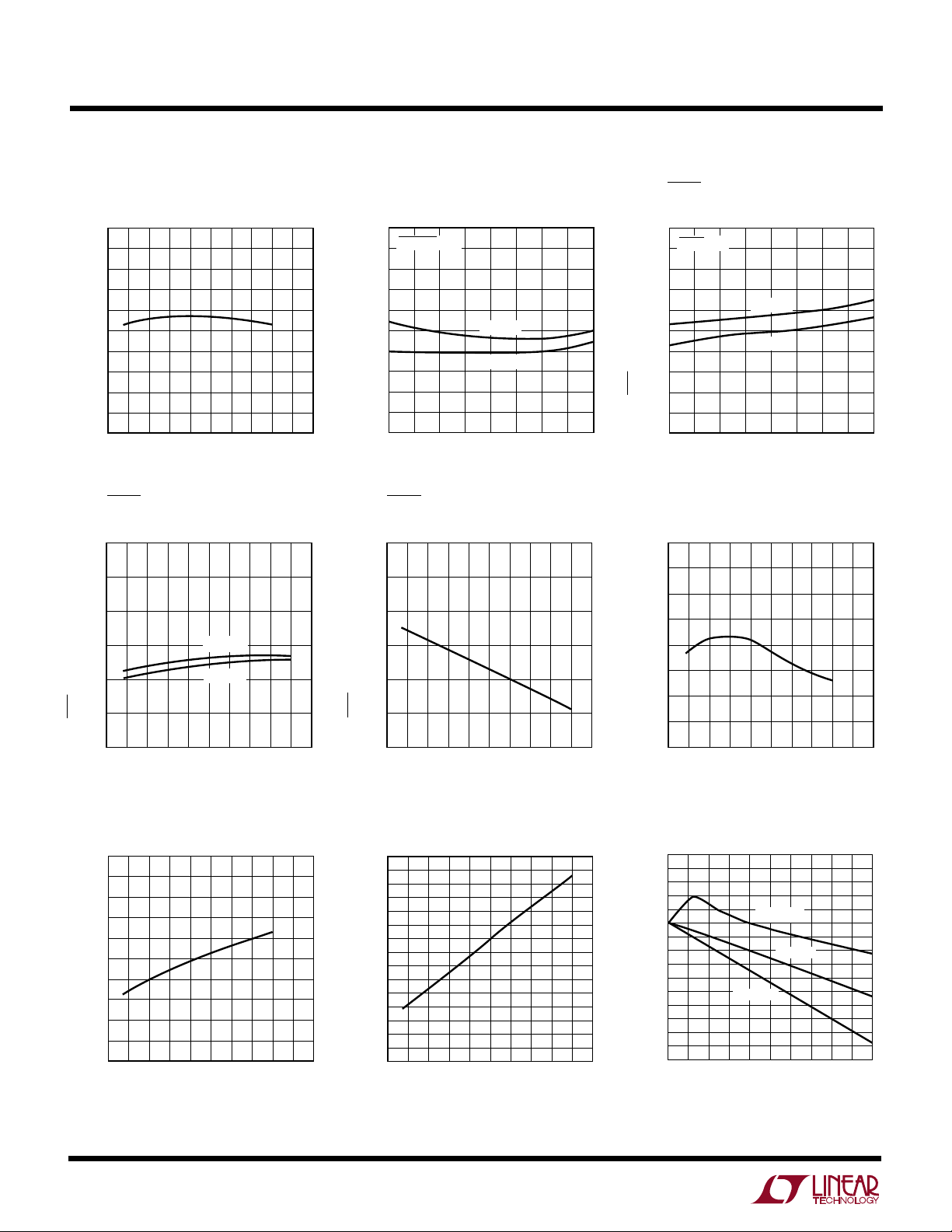
LT1786F
I
CCFL
PROGRAMMING CURRENT (µA)
5
4
3
2
1
0
–1
–2
–3
–4
–5
–6
–7
–8
–9
–10
40 80 120 160
1786 G09
20020060 100 140 180
T = –55°C
T = 25°C
T = 125°C
∆I
CCFL
SUMMING VOLTAGE (mV)
TEMPERATURE (°C)
–75
CCFL FREQUENCY (kHz)
220
240
125
1786 G06
200
180
160
–25
25
75
175
210
230
190
170
100
–50
0
50
150
W
U
TYPICAL PERFORMANCE CHARACTERISTICS
Supply Current
vs Temperature
10
9
8
7
6
5
4
3
SUPPLY CURRENT (mA)
2
1
0
–25–50 0 50 100 150
–75
25
TEMPERATURE (°C)
SHDN Input Bias Current
vs Temperature
6
5
4
3
75
VCC = 5V
125
1786 G01
175
ISUS Current vs Temperature
100
SMBSUS = 0V
90
8O
70
60
50
ISUS (µA)
40
30
20
10
0
–25–55 –5 50 100 150
VCC = 5V
VCC = 3V
25
TEMPERATURE (°C)
SHDN Threshold Voltage
vs Temperature
1.2
1.1
1.0
0.9
SHDN Supply Current
vs Temperature
300
SHDN = 0V
270
240
210
180
150
120
90
SHDN SUPPLY CURRENT (µA)
60
30
75
125
1786 G02
0
–25–55 –5 50 100 150
VCC = 5V
VCC = 3V
25
TEMPERATURE (°C)
75
125
1786 G03
Frequency vs Temperature
2
1
SHDN INPUT BIAS CURRENT (µA)
0
Maximum Duty Cycle
vs Temperature
95
93
91
89
87
85
83
81
79
CCFL MAXIMUM DUTY CYCLE (%)
77
75
–75
4
VCC = 3V
–25 25 75 125
TEMPERATURE (°C)
–25 0–50
25 50
TEMPERATURE (°C)
75 100
1786 G04
125 150
1786 G07
175–50–75 0 50 100 150
175
0.8
0.7
SHDN THRESHOLD VOLTAGE (V)
0.6
–25 25 75 125
TEMPERATURE (°C)
I
Summing Voltage
CCFL
vs Temperature
0.53
0.52
0.51
0.50
0.49
0.48
0.47
0.46
0.45
0.44
0.43
SUMMING VOLTAGE (V)
0.42
CCFL
0.41
I
0.40
0.39
0.38
–25 25 75 125
TEMPERATURE (°C)
1786 G05
1786 G08
175–50–75 0 50 100 150
I
Summing Voltage
CCFL
Load Regulation
175–50–75 0 50 100 150
Page 5
W
TEMPERATURE (°C)
0
POSITIVE DIO VOLTAGE (V)
0.4
0.2
0.8
0.6
1.2
1.0
–25 25 75 125
1786 G12
175–50–75 0 50 100 150
I(DIO) = 1mA
I(DIO) = 5mA
I(DIO) = 10mA
TEMPERATURE (°C)
0
CCFL V
C
LOW CLAMP VOLTAGE (V)
0.10
0.05
0.20
0.15
0.30
0.25
–25 25 75 125
1786 G15
175–50–75 0 50 100 150
TEMPERATURE (°C)
–75
BULB PROTECT SERVO VOLTAGE (V)
7.1
7.3
7.5
7.4
7.2
7.0
6.8
6.6
125 150
1786 G18
6.9
6.7
6.5
–25 0–50
25 50
75 100
175
I
CCFL
= 10µA
I
CCFL
= 50µA
I
CCFL
= 100µA
U
TYPICAL PERFORMANCE CHARACTERISTICS
LT1786F
VC Sink Offset Current
vs Temperature
10
9
8
7
6
5
4
3
2
1
SINK OFFSET CURRENT (µA)
C
0
–1
CCFL V
–2
–3
–25 0–50
–75 125 150
CCFL VC = 1.5V
CCFL VC = 1.0V
CCFL VC = 0.5V
75 100
25 50
TEMPERATURE (°C)
Negative DIO Voltage
vs Temperature
1.6
1.4
1.2
1.0
0.8
0.6
0.4
NEGATIVE DIO VOLTAGE (V)
0.2
0
–50
–75
I(DIO) = 10mA
I(DIO) = 5mA
I(DIO) = 1mA
–25
25
0
TEMPERATURE (°C)
75
50
100
125
150
1786 G13
175
1786 G10
175
∆CCFL VC Source Current for
∆I
Programming Current
CCFL
vs Temperature
5.10
5.05
I
= 100µA
5.00
4.95
SOURCE CURRENT FOR
4.90
C
PROGRAMMING CURRENT (µA/µA)
4.85
∆CCFL V
CCFL
∆I
4.80
CCFL
I
= 50µA
CCFL
I
CCFL
–25 25 75 125
TEMPERATURE (°C)
VC to DIO Current Servo Ratio
vs Temperature
103
102
101
100
99
98
97
DIO CURRENT SERVO RATIO (µA/mA)
C
96
CCFL V
95
–75
I(DIO) = 1mA
–50
I(DIO) = 10mA
–25
25
0
TEMPERATURE (°C)
= 10µA
I(DIO) = 5mA
75
50
100
125
1786 G11
150
1786 G14
Positive DIO Voltage
vs Temperature
175–50–75 0 50 100 150
VC Low Clamp Voltage
vs Temperature
175
VC High Clamp Voltage
vs Temperature
2.4
2.3
2.2
2.1
2.0
HIGH CLAMP VOLTAGE (V)
1.9
C
1.8
CCFL V
1.7
–75
–25
–50
0
TEMPERATURE (°C)
25
75 125
50
100
150
1786 G16
175
VC Switching Threshold
vs Temperature
1.3
1.2
1.1
1.0
0.9
0.8
SWITCHING THRESHOLD VOLTAGE (V)
C
0.7
CCFL V
0.6
–75
–50
0
25
–25
TEMPERATURE (°C)
75 125
50
100
150
BULB Protect Servo Voltage
vs Temperature
175
1786 G17
5
Page 6

LT1786F
TEMPERATURE (°C)
0.940
CCFL HIGH-SIDE SENSE NULL CURRENT (A)
0.980
0.960
1.020
1.000
1.060
1.040
–25 25 75 125
1786 G21
175–50
–75
0 50 100 150
DUTY CYCLE (%)
0
0
CCFL V
SW
CURRENT LIMIT (A)
0.5
1.5
2.0
2.5
20
40
50 90
1786 G24
1.0
10 30
60
70
80
T = 25°C
T = 125°C
MINIMUM
T = 0°C
TEMPERATURE (°C)
–50–75
FULL-SCALE OUTPUT CURRENT (µA)
0–25 5025
75
100 125 150 175
1786 G26
104
103
102
101
100
99
98
97
96
V(I
OUT
) = 0.465V
W
U
TYPICAL PERFORMANCE CHARACTERISTICS
BULB Input Bias Current
vs Temperature
10
8
6
4
2
BULB INPUT BIAS CURRENT (µA)
0
–50
–25 0
–75 125 150
TEMPERATURE (°C)
25 50
75 100
High-Side Sense Null Current Line
Regulation vs Temperature
0.160
0.140
0.120
0.100
0.080
0.060
0.040
0.020
CCFL HIGH-SIDE SENSE LINE REGULATI0N (%V)
0.000
–75
–50
–25
75
50
25
0
TEMPERATURE (°C)
100
125
1787 G19
150
1786 G22
175
175
High-Side Sense Supply Current
vs Temperature
150
140
130
120
110
100
90
80
70
60
CCFL HIGH-SIDE SENSE SUPPLY CURRENT (µA)
50
–50
–75
0
–25
25 50
TEMPERATURE (°C)
75 100
VSW Sat Voltage
vs Switch Current
1.0
0.9
0.8
0.7
0.6
0.5
SAT VOLTAGE (V)
0.4
SW
0.3
CCFL V
0.2
0.1
0
0.3
0
T = 25°C
0.9
0.6
SWITCH CURRENT (A)
125 150
T = –5°CT = 125°C
1.2
1786 G20
1787 G23
175
1.5
High-Side Sense Null Current
vs Temperature
V
Current Limit vs Duty Cycle
SW
6
Forced Beta vs ISW on V
110
100
90
80
70
60
50
FORCED BETA
40
30
20
10
0
0.4
0.6
0.2 1.8
0
1.2
0.8
1.0
CCFL ISW (A)
1.4
SW
1.6
Full-Scale Output Current
vs Temperature
2.0
1786 G25
Page 7

W
U
TYPICAL PERFORMANCE CHARACTERISTICS
LT1786F
DNL vs Code
1.0
0.8
0.6
0.4
0.2
0
DNL (LSB)
–0.2
–0.4
–0.6
–0.8
–1.0
0
16
32
CODE
48
64
1786 G27
UUU
PIN FUNCTIONS
CCFL PGND (Pin 1): This pin is the emitter of an internal
NPN power switch. CCFL switch current flows through
this pin and permits internal, switch-current sensing. The
regulator provides a separate analog ground and power
ground to isolate high current ground paths from low
current signal paths. Linear Technology recommends the
use of star-ground layout techniques.
I
(Pin 2): This pin is the input to the CCFL lamp current
CCFL
programming circuit. This pin internally regulates to
465mV. The pin accepts a DC input current signal of 0µ A
to 100µA full scale from the DAC. This input signal is
converted to a 0µ A to 500µ A source current at the CCFL V
pin. As input programming current increases, the regulated lamp current increases.
DIO (Pin 3): This pin is the common connection between
the cathode and anode of two internal diodes. The remaining terminals of the two diodes connect to ground. In a
grounded-lamp configuration, DIO connects to the low
voltage side of the lamp. Bidirectional lamp current flows
in the DIO pin and thus the diodes conduct alternately on
half cycles. Lamp current is controlled by monitoring onehalf of the average lamp current. The diode conducting on
negative half cycles has one-tenth of its current diverted to
the CCFL VC pin. This current nulls against the source
current provided by the lamp-current programmer circuit.
C
INL vs Code
1.0
0.8
0.6
0.4
0.2
0
INL (LSB)
–0.2
–0.4
–0.6
–0.8
–1.0
0
16
32
CODE
48
64
1786 G28
A single capacitor on the CCFL VC pin provides both stable
loop compensation and an averaging function to the halfwave-rectified sinusoidal lamp current. Therefore, input
programming current relates to one-half of average lamp
current. This scheme reduces the number of loop compensation components and permits faster loop transient
response in comparison to previously published circuits.
If a floating lamp configuration is used, ground the DIO
pin.
CCFL VC (Pin 4): This pin is the output of the lamp current
programmer circuit and the input of the current comparator for the CCFL regulator. Its uses include frequency
compensation, lamp-current averaging for grounded-lamp
circuits and current limiting. The voltage on the CCFL V
C
pin determines the current trip level for switch turn-off.
During normal operation this pin sits at a voltage between
0.95V (zero switch current) and 2.1V (maximum switch
current) with respect to analog ground (AGND). This pin
has a high impedance output and permits external voltage
clamping to adjust current limit. A single capacitor to
ground provides stable loop compensation. This simplified loop compensation method permits the CCFL regulator to exhibit single-pole transient response behavior and
virtually eliminates transformer output overshoot.
7
Page 8

LT1786F
UUU
PIN FUNCTIONS
AGND (Pin 5): This is the low current analog ground. It is
the negative sense terminal for the internal 1.24V reference and the I
Connect low current signal paths that terminate to ground
and frequency compensation components that terminate
to ground directly to this pin for best regulation and
performance.
SHDN (Pin 6): Pulling this pin low causes regulator
shutdown with quiescent current typically reduced to
150µA. In this condition, the DAC circuitry remains alive
and the DAC I
use a pull-up resistor to force a logic high level (maximum
of 6V). The pin can be floated and an internal current
source will pull the pin to a logic high level. However, poor
PCB layout techniques can permit switching noise to inject
into this pin and cause erratic operation. LTC recommends
the use of a pull-up resistor. If the SMBSUS pin is pulled
low or Bit 7 = 1 in the Command Byte, complete IC
shutdown is enabled. An internal open drain N-channel
device turns on and pulls the SHDN pin low. The N-channel
can sink up to 1.6mA.
SMBSUS (Pin 7): Pulling this pin low causes complete
shutdown for the IC with quiescent current typically
reduced to 40µA. In this SMBus suspend condition, the
DAC retains its last output current setting and returns to
this level when the logic low signal at this pin is removed.
If this pin is not used, use a pull-up resistor to force a
logic high level or tie it directly to VCC. Poor PCB layout
techniques can permit switching noise to inject into this
pin and cause erratic operation. A small value capacitor
may be required to filter out this noise. Setting Bit 7 = 1
in the Command Byte also enables an SMBus suspend
condition. Enabling an SMBus suspend condition turns
on an internal open drain N-channel device which pulls
the SHDN pin low. The N-channel device sinks up to
1.6mA at the SHDN pin.
ADR (Pin 8): This is the SMBus address select pin. Tie this
pin to either VCC or GND to select one of two SMBus
addresses to which the LT1786F will respond. If the ADR
OUT
summing voltage in the LT1786F.
CCFL
level is maintained. If this pin is not used,
pin is tied to GND, the SMBus address is set to 58 (HEX)
and the DAC I
is tied to VCC, the SMBus address is set to 5A (HEX) and
the DAC I
required for the DAC I
to keep the CCFL regulator off until the required value has
been programmed for the DAC via the SMBus.
SDA (Pin 9): This is the SMBus bidirectional data input and
digital output pin. Data is shifted into the SDA pin and
acknowledged by the SDA pin. SDA is a high impedance
pin while data is shifted into the pin and an open-drain
N-channel output during acknowledges. SDA requires a
pull-up resistor or current source to VCC.
SCL (Pin 10): This is the SMBus clock input pin. Data is
shifted into the SDA pin at the rising edges of the SCL clock
during data transfer. SCL is a high impedance pin. SCL
requires a pull-up resistor or current source to VCC.
I
OUT
provides a full-scale output current of 100µA ±4µA over
temperature. Initial accuracy is 100µA ±2µA.The pin can
be biased from –10V to (VCC – 1.3V). This pin is typically
tied directly to the I
current which sets the operating lamp current. The I
pin has very little bias voltage change when tied to the I
pin as I
sourced from the I
V
CC
IC accepts an input voltage range of 3V minimum to 6.5V
maximum with little change in quiescent current (zero
switch current). An internal, low-dropout regulator provides a 2.4V supply for most of the internal circuitry.
Supply current increases as switch current increases at a
rate approximately 1/50 of switch current. This corresponds to a forced Beta of 50 for the power switch. The IC
incorporates undervoltage lockout by sensing regulator
dropout and locking out switching for input voltages
below 2.5V. Hysteresis is not used to maximize the range
of input voltage. The typical input voltage is a 3.3V or 5V
logic supply.
OUT
(Pin 11): This pin is the current output for the DAC and
CCFL
(Pin 12): This is the supply pin for the LT1786F. The
powers up to zero scale. If the ADR pin
OUT
powers up to half scale. If a different value is
on power-up, use the SHDN pin
OUT
pin and provides the programming
CCFL
OUT
CCFL
is regulated. The programming current is
pin and sunk by the I
OUT
CCFL
pin.
8
Page 9

UUU
PIN FUNCTIONS
LT1786F
ROYER (Pin 13): This pin connects to the center-tapped
primary of the Royer converter and is used with the BAT
pin in a floating-lamp configuration where lamp current is
controlled by sensing Royer primary-side converter current. This pin is the inverting terminal of a high-side
current sense amplifier. The typical quiescent current is
50µA into the pin. If the CCFL regulator is not used in a
floating-lamp configuration, tie the Royer and BAT pins
together.
BAT (Pin 14): This pin connects to the battery or AC wall
adapter voltage from which the CCFL Royer converter
operates. This voltage is typically higher than the V
supply voltage but can equal V
The BAT voltage must be at least 2.1V greater than the
internal 2.4V regulator or 4.5V. This pin provides biasing
for the lamp-current programming block, is used with the
Royer pin for floating-lamp configurations and connects
to one input for the open-lamp protection circuitry. For
floating-lamp configurations, this pin is the noninverting
terminal of a high-side current sense amplifier. The typical
quiescent current is 50µ A into the pin. The BAT and Royer
pins monitor the primary-side Royer converter current
through an internal 0.1Ω topside current sense resistor. A
0A to 1A primary-side, center tap converter current is
translated to an input signal range of 0mV to 100mV for the
current sense amplifier. This input range translates to a
0µA to 500µA sink current at the CCFL VC pin that nulls
against the source current provided by the programmer
circuit. The BAT pin also connects to the topside of the
internal clamp between the BAT and BULB pins that is used
for open-lamp protection.
if VCC is a 5V logic supply.
CC
CC
BULB (Pin 15): This pin connects to the low side of a 7V
threshold comparator between the BAT and BULB pins.
This circuit sets the maximum voltage level across the
primary side of the Royer converter under all operating
conditions and limits the maximum secondary output
under start-up conditions or open-lamp conditions. This
eases transformer voltage rating requirements. Set the
voltage limit to ensure lamp start-up with worst-case,
lamp start voltages and cold temperature, system operating conditions. The BULB pin connects to the junction of
an external divider network. The divider network connects
from the center tap of the Royer transformer or the actual
battery supply voltage to the topside of the current source
“tail inductor.” A capacitor across the top of the divider
network filters switching ripple and sets a time constant
that determines how quickly the clamp activates. When
the comparator activates, sink current is generated to pull
the CCFL VC pin down. This action transfers the entire
regulator loop from current mode operation into voltage
mode operation.
CCFL V
NPN power switch for the CCFL regulator. The power
switch provides a minimum of 1.25A. Maximum switch
current is a function of duty cycle as internal slope compensation ensures stability with duty cycles greater than
50%. Using a driver loop to automatically adapt base drive
current to the minimum required to keep the switch in a
quasi-saturation state yields fast switching times and high
efficiency operation. The ratio of switch current to driver
current is about 50:1.
(Pin 16): This pin is the collector of the internal
SW
9
Page 10

LT1786F
BLOCK DIAGRAM
W
LT1786F SMBus Programmable CCFL Switching Regulator
SHDN
V
CC
12
6
SHUTDOWN
OUT
+
CCFL
2.4V
REGULATOR
200kHz
OSC
1×
Q3
2×
UNDER-
VOLTAGE
LOCKOUT
Q5
Q4
Q7
5×
9×
–
0µA TO 100µA FROM I
V1
0.465V
THERMAL
SHUTDOWN
D2
6V
Q6
2×
Q8
1×
Q9
3×
D1
Q11
R3
1k
ROYERBAT
13
14
CCFL
V
SW
16
R4
0.1Ω
–
g
m
LOGIC
+
COMP
DRIVE
ANTI-
SAT
Q1
+
CURRENT
AMP
R1
0.125Ω
–
GAIN = 4.4
Q10
2×
SCL
SDA
25
I
CCFL
10
9
SMBus
INTERFACE
8
ADR
AGND DIO
POWER-ON
RESET
1
REGISTER A
3-BIT LATCH
EN1
3
SD
1
6
BULB
SMBSUS
7
EN2
EN2
15
SHUTDOWN
REGISTER B
1-BIT LATCH
SD
REGISTER C
6-BIT LATCH
4
CCFL
V
C
SD
VOLTAGE
REFERENCE
R
ADJ
SD
6-BIT
6
CURRENT
DAC
1
CCFL
PGND
11
I
OUT
1786 BD
10
Page 11

LT1786F
UW
W
TI I G DIAGRA S
t
BUF
SDA
SCL
STARTSTOP
SMBus Write Byte Protocol, with SMBus Address = 0101101B,
ADR
SMBUS ADDRESS COMMAND BYTE DATA BYTE
SDA
0
1
1
Timing for SMBus Interface
START
t
HD:STA
t
t
LOW
HD:STA
t
r
t
HIGH
t
HD:DAT
t
f
t
SU:STA
t
SU:DAT
Operating Sequence
Command Byte = 0XXXXXXXB and Data Byte = 111111XXB
XXXXX X X 11 1 11 1X X
ACK
WR
SHDN
ACK
t
SU:STO
STOP
1786 TD01
ACK
V
GND
CC
SCL
I
OUT
S
102
S = START
P = STOP
* = OPTIONAL
3
4151607
8910
U
WUU
11 12 13 14 15 16 17 18 19 20 21 22 23 24 25
APPLICATIONS INFORMATION
Introduction
Current generation portable computers and instruments
use backlit Liquid Crystal Displays (LCDs). Cold Cathode
Fluorescent Lamps (CCFLs) provide the highest available
efficiency in back lighting the display. Providing the most
light out for the least amount of input power is the most
important goal. These lamps require high voltage AC to
operate, mandating an efficient high voltage DC/AC converter. The lamps operate from DC, but migration effects
damage the lamp and shorten its lifetime. Lamp drive
should contain zero DC component. In addition to good
efficiency, the converter should deliver the lamp drive in
the form of a sine wave. This minimizes EMI and RF
*
1786 TD02
P
FULL-SCALE
CURRENT
ZERO-SCALE
CURRENT
26 27
emissions. Such emissions can interfere with other
devices and can also degrade overall operating efficiency.
Sinusoidal CCFL drive maximizes current-to-light conversion in the lamp. The circuit should also permit lamp
intensity control from zero to full brightness with no
hysteresis or “pop-on.”
The small size and battery-powered operation associated
with LCD equipped apparatus dictate low component
count and high efficiency for these circuits. Size constraints place severe limitations on circuit architecture and
long battery life is a priority. Laptop and handheld portable
computers offer an excellent example. The CCFL and its
power supply can be responsible for almost 50% of the
11
Page 12

LT1786F
U
WUU
APPLICATIONS INFORMATION
battery drain. Additionally, all components, including PC
board and hardware, usually must fit within the LCD
enclosure with a height restriction of 5mm to 10mm.
The CCFL regulator drives an inductor that acts as a
switched-mode current source for a current-driven Royerclass converter with efficiencies as high as 90%. The
control loop forces the CCFL PWM to modulate the average inductor current to maintain constant current in the
lamp. The constant current value, and thus lamp intensity,
is programmable. This drive technique provides a wide
range of intensity control. A unique lamp-current programming block permits either grounded lamp or floating
lamp configurations. Grounded lamp circuits directly sense
one-half of average lamp current. Floating lamp circuits
directly sense the Royer’s primary-side converter current.
Floating-lamp circuits provide symmetric differential drive
to the lamp and reduce the parasitic loss from stray lampto-frame capacitance, extending illumination range.
Block Diagram Operation
The LT1786F is a fixed frequency, current mode switching
regulator. A fixed frequency, current mode switcher controls switch duty cycle directly by switch current rather
than by output voltage. Referring to the block diagram for
the LT1786F, the switch turns ON at the start of each
oscillator cycle. The switch turns OFF when switch current
reaches a predetermined level. The control of output lamp
current is obtained by using the output of a unique
programming block to set current trip level. The current
mode switching technique has several advantages. First,
it provides excellent rejection of input voltage variations.
Second, it reduces the 90° phase shift at mid-frequencies
in the energy storage inductor. This simplifies closed-loop
frequency compensation under widely varying input
voltage or output load conditions. Finally, it allows simple
pulse-by-pulse current limiting to provide maximum
switch protection under output overload or short-circuit
conditions.
The LT1786F incorporates a low dropout internal regulator that provides a 2.4V supply for most of the internal
circuitry. This low dropout design allows input voltage to
vary from 3V to 6.5V with little change in quiescent
current. An active low shutdown pin typically reduces total
supply current to 150µ A by shutting off the 2.4V regulator
and locks out switching action for standby operation. The
IC incorporates undervoltage lockout by sensing regulator
dropout and locking out switching below about 2.5V. The
regulator also provides thermal shutdown protection that
locks out switching in the presence of excessive junction
temperatures.
A 200kHz oscillator is the basic clock for all internal timing.
The oscillator turns on the output switch via its own logic
and driver circuitry. Adaptive anti-sat circuitry detects the
onset of saturation in the power switch and adjusts base
drive current instantaneously to limit switch saturation.
This minimizes driver dissipation and provides rapid turnoff of the switch. The CCFL power switch is guaranteed to
provide a minimum of 1.25A in the LT1786F. The antisat
circuitry provides a ratio of switch current to driver current
of about 50:1.
Digital Interface
The LT1786F communicates with an SMBus host using
the standard 2-wire SMBus interface. The Timing Diagram
shows the signals on the SMBus. The two bus lines SDA
and SCL must be high when the bus is not in use. External
pull-up resistors or current sources are required at these
lines.
The LT1786F is a receive-only (slave) device. The master
must apply the following Write Byte protocol to communicate with the LT1786F:
17 1181811
S Slave Address WR A Command Byte A Data Byte A P
S = Start Conditon, WR = Write Bit, A = Acknowledge Bit, P = Stop Condition
The master initiates communication with the LT1786F
with a START condition (see SMBus Operating Sequence)
and a 7-bit address followed by the write bit = 0. The
LT1786F acknowledges and the master delivers the
command byte. The LT1786F acknowledges and latches
the active bits of the command byte into register A (see
Block Diagram) at the falling edge of the acknowledge
pulse. The master sends the data byte and the LT1786F
acknowledges the data byte. The data byte is latched into
register C at the falling edge of the final acknowledge pulse
and the DAC current output assumes the new 6-bit data
12
Page 13

LT1786F
U
WUU
APPLICATIONS INFORMATION
value (see Block Diagram). A STOP condition is optional.
The command code and data byte are defined with the
following format:
Command Code
7 6543210 76543210
SHDN X X X X X X X D5 D4 D3 D2 D1 D0 X X
SHDN: 0 for normal operation, 1 for shutdown
D5 to D0: DAC Data Byte Bits, D5 is the Most Significant Bit
START and STOP Conditions
At the beginning of any SMBus communication, the master must transmit a START condition by switching SDA
from high to low while SCL is high. When a master has
finished communicating with a slave device, a STOP
condition is issued by switching SDA from low to high
while SCL is high. The SMBus is then free for communication with another SMBus device.
Early STOP Conditions
The LT1786F recongnizes a STOP condition at any point in
the SMBus communication sequence. If the STOP occurs
prematurely before the data byte is acknowledged in the
Write Byte protocol, the DAC output current value is not
updated; otherwise internal register C is updated with the
new data and the DAC output current changes
correspondingly.
Data Byte
6-Bit Current Output DAC
The 6-bit current output DAC is guaranteed monotonic and
is digitally adjustable in 63 equal steps. On power-up, if
ADR connects to VCC, the 6-bit internal register C (see
Block Diagram) resets to 100000B and the DAC output is
set to midrange. On power-up, if ADR connects to ground,
register C resets to 000000B and the DAC output is set to
zero. For the LT1786F, the current source output (I
can be biased from –10V to (VCC – 1.3V). Full-scale
current is trimmed to ±2% at room temperature and ±4%
over the commercial temperature range.
Shutdown
Three methods may be employed to shut down the LT1786F
(see Block Diagram).
The LT1786F enters SMBus suspend mode if a logic low
level is applied to the SMBSUS pin or a logic high level is
applied to Bit 7 in the Command Byte of the SMBus
communication sequence. In SMBus suspend mode, supply current typically drops to 40µA and the last output
current setting is internally retained. The DAC resumes
this level upon its return to normal operation. Enabling an
SMBus suspend condition also turns on an open-drain
N-channel MOSFET which pulls the SHDN pin low. The
N-channel device sinks up to 1.6mA at the SHDN pin and
its logic low level is guaranteed to less than 0.4V.
OUT
)
The Slave Address
The LT1786F responds to one of two 7-bit addresses. The
first five bits have been factory programmed to 01011. The
last two address bits are programmed by the user by tying
the ADR pin to VCC or GND (see functional table)
ADR SMBus ADDRESS DAC POWER-UP VALUE
GND 0101101 Zero Scale
V
CC
0101100 Midscale
The LT1786F enters regulator shutdown mode if a logic
low level is applied to the SHDN pin. In this mode, supply
current typically drops to 150µ A, the switching regulator
circuitry is shut down and the DAC is kept alive. The DAC
output current setting is maintained. This feature can be
used to program the DAC to a desired output current level
(other than the preset zero-scale or midscale level defined
by the selected SMBus address) before allowing the CCFL
regulator to turn on.
13
Page 14

LT1786F
U
WUU
APPLICATIONS INFORMATION
LT1786F SMBus Lookup Tables
SMBus Address Byte Table
ADR DECIMAL BINARY HEX I
GND 91 0101101 5A Zero Scale
V
CC
Bit 0 (LSB) in the SMBus Address is the Write Bit = 0
88 0101100 58 Midscale
SMBus Data Byte Table
DECIMAL BINARY HEX I
0 000000XX 00-03 0.000
1 000001XX 04-07 1.587
2 000010XX 08-0B 3.175
3 000011XX 0C-0F 4.762
4 000100XX 10-13 6.349
5 000101XX 14-17 7.937
6 000110XX 18-1B 9.524
7 000111XX 1C-1F 11.111
8 001000XX 20-23 12.698
9 001001XX 24-27 14.286
10 001010XX 28-2B 15.873
11 001011XX 2C-2F 17.460
12 001100XX 30-33 19.048
13 001101XX 34-37 20.635
14 001110XX 38-3B 22.222
15 001111XX 3C-3F 23.810
16 010000XX 40-43 25.397
17 010001XX 44-47 26.984
18 010010XX 48-4B 28.571
19 010011XX 4C-4F 30.159
20 010100XX 50-53 31.746
21 010101XX 54-57 33.333
22 010110XX 58-5B 34.921
23 010111XX 5C-5F 36.508
24 011000XX 60-63 38.095
25 011001XX 64-67 39.683
26 011010XX 68-6B 41.270
27 011011XX 6C-6F 42.857
28 011100XX 70-73 44.444
29 011101XX 74-77 46.032
30 011110XX 78-7B 47.619
31 011111XX 7C-7F 49.206
X = Don’t Care, I
= Ideal Value
OUT
POWER-UP VALUE
OUT
OUT
(µA)
SMBus Command Byte Table
DECIMAL BINARY HEX MODE
0-127 0XXXXXXX 00-7F Normal
128-255 1XXXXXXX 80-FF Shutdown
X = Don’t Care
DECIMAL BINARY HEX I
32 100000XX 80-83 50.794
33 100001XX 84-87 52.381
34 100010XX 88-8B 53.968
35 100011XX 8C-8F 55.556
36 100100XX 90-93 57.143
37 100101XX 94-97 58.730
38 100110XX 98-9B 60.317
39 100111XX 9C-9F 61.905
40 101000XX A0-A3 63.492
41 101001XX A4-A7 65.079
42 101010XX A8-AB 66.667
43 101011XX AC-AF 68.254
44 101100XX B0-B3 69.841
45 101101XX B4-B7 71.429
46 101110XX B8-BB 73.016
47 101111XX BC-BF 74.603
48 110000XX C0-C3 76.190
49 110001XX C4-C7 77.778
50 110010XX C8-CB 79.365
51 110011XX CC-CF 80.952
52 110100XX D0-D3 82.540
53 110101XX D4-D7 84.127
54 110110XX D8-DB 85.714
55 110111XX DC-DF 87.302
56 111000XX E0-E3 88.889
57 111001XX E4-E7 90.476
58 111010XX E8-EB 92.063
59 111011XX EC-EF 93.651
60 111100XX F0-F3 95.238
61 111101XX F4-F7 96.825
62 111110XX F8-FB 98.413
63 111111XX FC-FF 100.000
OUT
(µA)
14
Page 15

LT1786F
I
OUT
FULL-SCALE
100µA
V(I
CCFL
)
465mV
I
XI
V1
R1
V
REF
R3
I = 100µA
0 < X < 1
SELECT V1 WITHIN THE DAC I
OUT
COMPLIANCE RANGE
(EX. V1 = 2V FOR V
CC
= 3.3V OR 5V)
CHOOSE I1 >> (1 – X)I
R1 = (V1 – 0.465)/[(X)(100µA)]
R2 = (V1 – 0.465)/[(1 – X)(100µA)]
R3 = (V
REF
– 0.465)/I1
R4 = 0.465R3/[(1 – X)(100µA)(R3)
+ (V
REF
– 0.465)]
I1
1786 F01
R4
V(I
CCFL
)
(1 – X)I
R2
U
WUU
APPLICATIONS INFORMATION
Simplified Lamp Current Programming
A programming block in the LT1786F controls lamp
current, permitting either grounded lamp or floating lamp
configurations. Grounded configurations control lamp
current by directly controlling one-half of actual lamp
current and converting it to a feedback signal to close a
control loop. Floating configurations control lamp current
by directly controlling the Royer’s primary-side converter
current and generating a feedback signal to close a control
loop.
Previous backlighting solutions have used a traditional
error amplifier in the control loop to regulate lamp current.
This approach converted an RMS current into a DC voltage
for the input of the error amplifier. This approach used
several time constants in order to provide stable loop
frequency compensation. This compensation scheme
meant that the loop had to be fairly slow and that output
overshoot with start-up or overload conditions had to be
carefully evaluated in terms of transformer stress and
breakdown voltage requirements.
of the probe’s respective input capacitance. A current
meter in series with the I
pin will also produce oscil-
CCFL
lation due to its shunt capacitance. Use a decoupling
resistor of several kilohms between the I
I
pin if excessive trace stray capacitance exists. Nor-
OUT
pin and the
CCFL
mally, this resistor is not required.
In some applications, the maximum programming current
required at the I
pin for a maximum lamp current will be
CCFL
less than the full-scale output current of the DAC, which is
100µA. The system designer can either limit the maximum
programming current through software built into the system,
or use a current splitter which shunts a percentage of the fullscale current from the I
pin. A splitter circuit is illustrated
CCFL
in Figure 1. A divider string is used from a reference voltage
to set up a voltage level equal to the I
summing voltage,
CCFL
or 465mV. The main current flowing in the divider string
should be chosen to swamp out the effects of the shunted
current into the divider string.
The LT1786F eliminates the error amplifier concept
entirely and replaces it with a lamp current programming
block. This block provides an easy-to-use interface to
program lamp current. The programmer circuit also
reduces the number of time constants in the control loop
by combining the error signal conversion scheme and
frequency compensation into a single capacitor. The control loop thus exhibits the response of a single pole
system, allows for faster loop transient response and
virtually eliminates overshoot under start-up or overload
conditions.
Lamp current is programmed at the input of the programmer block, the I
pin. This pin is the input of a shunt
CCFL
regulator and accepts a DC input current signal of 0µ A to
100µ A from the DAC. This input signal is converted to a
0µA to 500µA source current at the CCFL VC pin. The
programmer circuit is simply a current-to-current converter with a gain of five.
The I
pin is sensitive to capacitive loading and will
CCFL
oscillate with capacitance greater than 10pF. For example,
loading the I
oscillation and erratic CCFL regulator operation because
pin with a 1× or 10× scope probe causes
CCFL
Figure 1
Grounded Lamp Configuration
In a grounded lamp configuration, the low voltage side of
the lamp connects directly to the LT1786F DIO pin. This
pin is the common connection between the cathode and
anode of two internal diodes. In previous grounded lamp
solutions, these diodes were discrete units and are now
integrated onto the IC, saving cost and board space.
Bidirectional lamp current flows in the DIO pin and thus,
the diodes conduct alternately on half cycles. Lamp current is controlled by monitoring one-half of the average
lamp current. The diode conducting on negative half
cycles has one-tenth of its current diverted to the CCFL V
C
pin and nulls against the source current provided by the
15
Page 16

LT1786F
U
WUU
APPLICATIONS INFORMATION
lamp current programmer circuit. The compensation capacitor on the CCFL VC pin provides stable loop compensation and an averaging function to the rectified sinusoidal
lamp current. Therefore, input programming current relates to one-half of average lamp current.
The transfer function between lamp current and input
programming current must be empirically determined and
is dependent on the particular lamp/display housing combination used. The lamp and display housing are a distributed loss structure due to parasitic lamp-to-frame capacitance. This means that the current flowing at the highvoltage side of the lamp is higher than what is flowing at
the DIO pin side of the lamp. The input programming
current is set to control lamp current at the high-voltage
side of the lamp, even though the feedback signal is the
lamp current at the bottom of the lamp. This ensures that
the lamp is not overdriven which can degrade the lamp’s
operating lifetime. Therefore, the full scale current of the
DAC does not necessarily correspond to the current
required to set maximum lamp current.
Floating Lamp Configuration
In a floating lamp configuration, the lamp is fully floating
with no galvanic connection to ground. This allows the
transformer to provide symmetric differential drive to the
lamp. Balanced drive eliminates the field imbalance associated with parasitic lamp-to-frame capacitance and reduces “thermometering” (uneven lamp intensity along the
lamp length) at low lamp currents.
Carefully evaluate display designs in relation to the physical layout of the lamp, its leads and the construction of the
display housing. Parasitic capacitance from any high
voltage point to DC or AC ground creates paths for
unwanted current flow. This parasitic current flow
degrades electrical efficiency and losses up to 25% have
been observed in practice. As an example, at a Royer
operating frequency of 60kHz, 1pF of stray capacitance
represents an impedance of 2.65MΩ. With an operating
lamp voltage of 400V and an operating lamp current of
6mA, the parasitic current is 150µA. This additional cur-
rent must be supplied by the transformer secondary.
Layout techniques that increase parasitic capacitance
include long high voltage lamp leads, reflective metal foil
around the lamp and displays supplied in metal enclosures. Losses for a good display are under 5%, whereas,
losses for a bad display range from 5% to 25%. Lossy
displays are the primary reason to use a floating lamp
configuration. Providing symmetric, differential drive to
the lamp reduces the total parasitic loss by one-half.
Maintaining closed-loop control of lamp current in a
floating lamp configuration necessitates deriving a feedback signal from the primary side of the Royer transformer. Previous solutions have used an external precision shunt and high-side sense amplifier configuration.
This approach has been integrated onto the LT1786F for
simplicity of design and ease of use. An internal 0.1Ω
resistor monitors the Royer converter current and connects between the input terminals of a high-side sense
amplifier. A 0 – 1 Amp Royer primary-side, center-tap
current is translated to a 0µ A to 500µA sink current at the
CCFL VC pin to null against the source current provided by
the lamp current programmer circuit. The compensation
capacitor on the CCFL VC pin provides stable loop compensation and an averaging function to the error sink
current. Therefore, input programming current is related
to average Royer converter current. Floating lamp circuits
operate similarly to grounded lamp circuits except for the
derivation of the feedback signal.
The transfer function between lamp current and input
programming current must be empirically determined and
is dependent upon a myriad of factors including lamp
characteristics, display construction, transformer turns
ratio and the tuning of the Royer oscillator. Once again,
lamp current will be slightly higher at one end of the lamp
and input programming current should be set for this
higher level to ensure that the lamp is not overdriven.
The internal 0.1Ω high-side sense resistor on the LT1786F
is rated for a maximum DC current of 1A. This resistor can
be damaged by extremely high surge currents at start-up.
The Royer converter typically uses a few microfarads of
bypass capacitance at the center tap of the transformer.
This capacitor charges up when the system is first powered by the battery pack or an AC wall adapter. The amount
of current delivered at start-up can be very large if the total
impedance in this path is small and the voltage source has
high current capability. Linear Technology recommends
16
Page 17

LT1786F
U
WUU
APPLICATIONS INFORMATION
the use of an aluminum electrolytic for the transformer
center-tap bypass capacitor with an ESR greater than or
equal to 0.5Ω. This lowers the peak surge currents to an
acceptable level. In general, the wire and trace inductance
in this path also help reduce the di/dt of the surge current.
This issue only exists with floating lamp circuits as
grounded lamp circuits do not make use of the high-side
sense resistor.
Input Capacitor Type
Caution must be used in selecting the input capacitor type
for switching regulators. Aluminum electrolytics are electrically rugged and the lowest cost, but are physically large
to meet required ripple current ratings, and size constraints (especially height) may preclude their use. Ceramic capacitors are now available in larger values and
their high ripple current and voltage rating make them
ideal for input bypassing.
Solid tantalum capacitors would be a good choice except
for a history of occasional failure when subjected to large
current surges during start-up. The input bypass capacitor of regulators can see these high surges when a battery
or high capacitance source is connected. Some manufacturers have developed tantalum capacitor lines specially
tested for surge capability (AVX TPS series for instance),
but even these units may fail if the input voltage surge
approaches the capacitor’s maximum voltage rating. AVX
recommends derating the capacitor voltage by 2:1 for high
surge applications.
Applications Support
Linear Technology invests an enormous amount of time,
resources and technical expertise in understanding,
designing and evaluating backlight/LCD contrast solutions for system designers. The design of an efficient and
compact LCD backlight system is a study of compromise
in a transduced electronic system. Every aspect of the
design is interrelated and any design change requires
complete re-evaluation for all other critical design parameters. Linear Technology has engineered one of the most
complete test and evaluation setups for backlight designs
and understands the issues and tradeoffs in achieving a
compact, efficient and economical customer solution.
Linear Technology welcomes the opportunity to discuss,
design, evaluate and optimize any backlight/LCD contrast
system with a customer. For further information on backlight/LCD contrast designs, consult the References.
References
1. Williams, Jim. August 1992.
Liquid Crystal Displays
Application Note 49.
2. Williams, Jim. August 1993.
cient LCD Illumination
Application Note 55.
3. Bonte, Anthony. March 1995.
with Dual Polarity Contrast
tion, Design Note 99.
4. Williams, Jim. April 1995.
rent Probe for LCD Backlight Measurement
nology Corporation, Design Note 101.
5. LT1182/LT1183/LT1184/LT1184F Data Sheet.
LCD Contrast Switching Regulators
Technology Corporation.
6. Williams, Jim. November 1995.
LCD Backlight Technology
tion, Application Note 65.
. Linear Technology Corporation,
. Linear Technology Corporation,
Illumination Circuitry for
Techniques for 92% Effi-
LT1182 Floating CCFL
. Linear Technology Corpora-
A Precision Wideband Cur-
. Linear Tech-
CCFL/
. April 1995. Linear
A Fourth Generation of
. Linear Technology Corpora-
17
Page 18

LT1786F
TYPICAL APPLICATION
U
Dual Transformer CCFL Power Supply
Space constraints may dictate utilization of two small
transformers instead of a single, larger unit. Although this
approach is somewhat more expensive, it can solve space
problems and offers other attractive advantages. Figure
2’s approach is essentially a “grounded lamp” LT1786Fbased circuit. The transistors drive two transformer primaries in parallel. The transformer secondaries, stacked
in series, provide the output. The relatively small transformers, each supplying half the load power, may be
located directly at the lamp terminals. Aside from the
obvious space advantage (particularly height), this
arrangement minimizes parasitic wiring losses by elimi-
10
1000pF
3
220k
21
+
2.2µF
0.1µF*
nating high voltage lead length. Additionally, although the
lamp receives differential drive, with its attendant low
parasitic losses, the feedback signal is ground referred.
Thus, the stacked secondaries afford floating lamp operating efficiency with grounded mode current certainty and
line regulation.
L1 is directly driven, with winding 4-5 furnishing feedback
in the normal fashion. L3, “slaved” to L1’s and L3’s
interconnects must be laid out for low inductance to
maintain waveform purity. The traces should be as wide as
possible (e.g., 1/8") and overlaid to cancel inductive
effects.
27pF
LAMP
6
+
10
2
2.2µF
4
1
NC NC
L3
5
6
L1
4
5
WIDE TRACE
SEE TEXT AND NOTES
WIDE TRACE
3
0.1µF*
SHUTDOWN
1µF
1
2
3
4
5
6
7
8
100k
PGND
I
CCFL
DIO
V
C
AGND
SHDN
SMBSUS
ADR
LT1786F
BAT54
ROYER
V
SW
BULB
BAT
V
I
OUT
SCL
SDA
Q1-Q2
ZDT1048
L2
16
15
14
13
12
IN
11
10
9
+
2.2µF
16V
TO
SMBus
HOST
750Ω
MBRS130L
L1, L3 = COILTRONICS CTX110605
OVERLAY INDICATED TRACES BETWEEN L1 AND L3
L2 = COILTRONICS CTX100-4
* = WIMA MKI OR MKP-20
= PANASONIC ECH-U
COILTRONICS (561) 241-7876
+V
BAT
V
IN
5V
Figure 2. Dual Transformers Save Space and Minimize parasitic Losses While Maintaining
Current Accuracy and Line Regulation. Trade-Off Is Increased Cost
1786 F02
18
Page 19

PACKAGE DESCRIPTION
16-Lead Plastic Small Outline (Narrow 0.150)
U
Dimensions in inches (millimeters) unless otherwise noted.
S Package
(LTC DWG # 05-08-1610)
0.386 – 0.394*
(9.804 – 10.008)
13
16
14
15
12
11 10
LT1786F
9
0.010 – 0.020
(0.254 – 0.508)
0.008 – 0.010
(0.203 – 0.254)
*
DIMENSION DOES NOT INCLUDE MOLD FLASH. MOLD FLASH
SHALL NOT EXCEED 0.006" (0.152mm) PER SIDE
**
DIMENSION DOES NOT INCLUDE INTERLEAD FLASH. INTERLEAD
FLASH SHALL NOT EXCEED 0.010" (0.254mm) PER SIDE
× 45°
0° – 8° TYP
0.016 – 0.050
0.406 – 1.270
0.228 – 0.244
(5.791 – 6.197)
0.053 – 0.069
(1.346 – 1.752)
0.014 – 0.019
(0.355 – 0.483)
0.150 – 0.157**
(3.810 – 3.988)
4
5
0.050
(1.270)
TYP
3
2
1
7
6
8
0.004 – 0.010
(0.101 – 0.254)
S16 0695
Information furnished by Linear Technology Corporation is believed to be accurate and reliable.
However, no responsibility is assumed for its use. Linear Technology Corporation makes no representation that the interconnection of its circuits as described herein will not infringe on existing patent rights.
19
Page 20

LT1786F
TYPICAL APPLICATION
90% Efficient Grounded CCFL with 2-Wire SMBus Control of Lamp Current
U
C7
1µF
SHUTDOWN
1
2
3
4
5
6
7
8
CCFL
PGND
I
CCFL
DIO
CCFL V
AGND
SHDN
SMBSUS
ADR
D1
BAT85
CCFL V
LT1786F
C
SW
BULB
BAT
ROYER
V
I
OUT
SCL
SDA
1000pF
CC
LAMP
10
6
321 5
C5
16
15
14
13
12
11
10
9
R2
221k
1%
R3
100k
1%
+
TO
SMBus
HOST
C4
2.2µF
+
C1
0.068µF
Q2 Q1
L2
100µH
3V < V
CC
< 6.5V
C2
27pF
3kV
L1
4
C3
2.2µF
35V
R1
750Ω
1%
D1
1N5818
C1 MUST BE A LOW LOSS CAPACITOR
C1 = WIMA MKI OR MKP-20
PANASONIC ECH-U
L1 = COILTRONICS CTX210605
L2 = COILTRONICS CTX100-4
(DO NOT SUBSTITUTE COMPONENTS
COILTRONICS (561) 241-7876)
Q1, Q2 = ZETEX ZTX849 OR ROHM 25C5001
BAT
8V TO 28V
1786F TA03
RELATED PARTS
PART NUMBER DESCRIPTION COMMENTS
LT1172 Current Mode Switching Regulator for CCFL or LCD Contrast Control 1.25A, 100kHz
LT1173 Micropower DC/DC Converter for LCD Contrast Control 1A, 24kHz, Hysteretic
LT1182 Dual Current Mode Switching Regulator for CCFL and LCD Contrast Control 1.25A, 0.625A, 200kHz
LT1183 Dual Current Mode Switching Regulator for CCFL and LCD Contrast Control 1.25A, 0.625A, 200kHz
LT1184 Current Mode Switching Regulator for CCFL Control 1.25A, 200kHz
LT1184F Current Mode Switching Regulator for CCFL Control 1.25A, 200kHz
LT1186F DAC Programmable Current Mode Switching Regulator for CCFL Control 1.25A, 200kHz, SPI or Pulse Mode
LT1316 Micropower DC/DC Converter for LCD Contrast Control Programmable Peak Current Limit
LT1372 Current Mode Switching Regulator for CCFL or LCD Contrast Contol 1.5A, 500kHz
1786f LT/TP 0898 4K • PRINTED IN USA
LINEAR TECHNOLOGY CORPORATION 1998
20
Linear Technology Corporation
1630 McCarthy Blvd., Milpitas, CA 95035-7417
(408) 432-1900 ● FAX: (408) 434-0507
●
www.linear-tech.com
 Loading...