

Page 1
FEATURES
–900 –600 –300 0 300 600 900
PERCENTAGE OF AMPLIFIERS
INPUT OFFSET VOLTAGE (µV)
1782 G25
25
20
15
10
5
0
VS = 5V, 0V
V
CM
= 2.5V
LT1783
1.25MHz, Over-The-Top
Micropower, Rail-to-Rail
Input and Output Op Amp in SOT-23
U
DESCRIPTIO
■
Operates with Inputs Above V
■
Rail-to-Rail Input and Output
■
Micropower: 300µA Supply Current Max
■
Small SOT-23 Package
■
Gain Bandwidth product: 1.25MHz
■
Slew Rate: 0.42V/µs
■
Low Input Offset Voltage: 800µV Max
■
Single Supply Input Range: 0V to 18V
■
High Output Current: 18mA Min
■
Specified on 3V, 5V and ±5V Supplies
■
Output Shutdown on 6-Lead Version
■
Reverse Battery Protection to 18V
■
High Voltage Gain: 1500V/mV
■
Operating Temperature Range: –40°C to 85°C
+
U
APPLICATIO S
■
Portable Instrumentation
■
Battery- or Solar-Powered Systems
■
Sensor Conditioning
■
Supply Current Sensing
■
Battery Monitoring
■
MUX Amplifiers
■
4mA to 20mA Transmitters
The LT®1783 is a 1.25MHz op amp available in the small
SOT-23 package that operates on all single and split
supplies with a total voltage of 2.5V to 18V. The amplifier
draws less than 300µA of quiescent current and has
reverse battery protection, drawing negligible current for
reverse supply voltages up to 18V.
The input range of the LT1783 includes ground, and a
unique feature of this device is its Over-The-TopTM operation capabilitity with either or both of its inputs above the
positive rail. The inputs handle 18V both differential and
common mode, independent of supply voltage. The input
stage incorporates phase reversal protection to prevent
false outputs from occurring even when the inputs are 9V
below the negative supply.
The LT1783 can drive loads up to 18mA and still maintain
rail-to-rail capability. A shutdown feature on the 6-lead
version can disable the part, making the output high
impedance and reducing quiescent current to 5µA. The
LT1783 op amp is available in the 5- and 6-lead
SOT-23 packages. For applications requiring lower power,
refer to the LT1782.
, LTC and LT are registered trademarks of Linear Technology Corporation.
Over-The-Top is a trademark of Linear Technology Corporation.
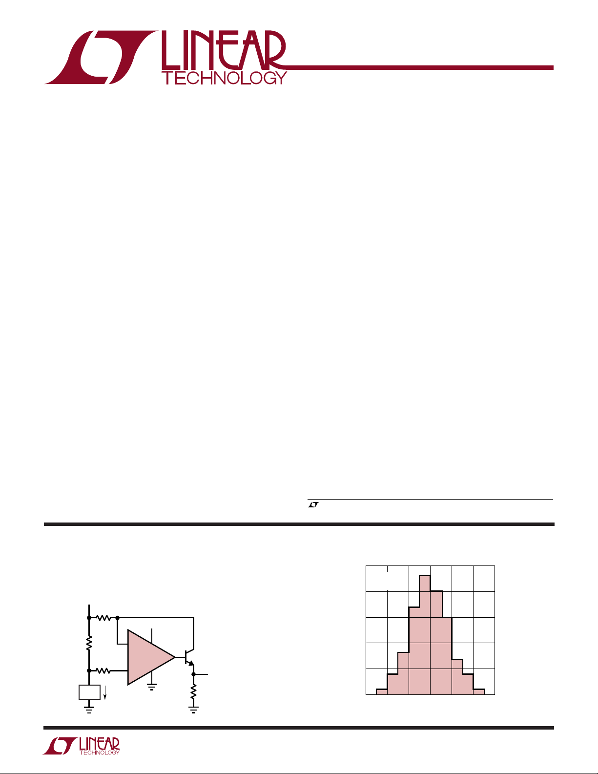
TYPICAL APPLICATIO
Positive Supply Rail Current Sense
+
V
5V TO 18V
LOAD
200Ω
0.2Ω
200Ω
I
LOAD
+
LT1783
–
U
Distribution of Input Offset Voltage
5V
2N3904
V
0V TO 4.3V
2k
OUT
1783 TA01
= 2Ω(I
LOAD
)
1
Page 2
LT1783
WW
W
ABSOLUTE MAXIMUM RATINGS
Total Supply Voltage (V+ to V–) .............................. 18V
Input Differential Voltage ........................................ 18V
Input Pin Voltage to V–............................... +24V/– 10V
Shutdown Pin Voltage Above V–............................ 18V
Shutdown Pin Current ....................................... ±10mA
U
(Note 1)
Operating Temperature Range (Note 10) –40°C to 85°C
Specified Temperature Range ......................
Junction Temperature........................................... 150°C
Storage Temperature Range ................ –65°C to 150°C
Lead Temperature (Soldering, 10 sec)................. 300°C
Output Short-Circuit Duration (Note 2) ........... Indefinite
U
W
U
PACKAGE/ORDER INFORMATION
TOP VIEW
+
1
OUT
–
2
V
+IN
T
JMAX
Consult factory for Industrial and Military grade parts.
+
3
S5 PACKAGE
5-LEAD PLASTIC SOT-23
= 150°C, θJA = 250°C/ W
5
V
–
–IN
4
ORDER PART
LT1783CS5
S5 PART MARKING S6 PART MARKING
NUMBER
LTLF
OUT
+IN
TOP VIEW
1
–
2
V
6-LEAD PLASTIC SOT-23
T
JMAX
+
3
–
S6 PACKAGE
= 150°C, θJA = 230°C/ W
+
ORDER PART
V
6
SHDN
5
–IN
4
NUMBER
LT1783CS6
ELECTRICAL CHARACTERISTICS
The ● denotes specifications which apply over the specified temperature range, otherwise specifications are TA = 25°C.
VS = 3V, 0V; VS = 5V, 0V, VCM = V
= half supply, for the 6-lead part V
OUT
= 0V, pulse power tested unless otherwise specified.
PIN5
0°C to 70°C
LTIU
SYMBOL PARAMETER CONDITIONS MIN TYP MAX UNITS
V
OS
I
OS
I
B
e
n
i
n
R
IN
C
IN
CMRR Common Mode Rejection Ratio VCM = 0V to VCC – 1V ● 90 100 dB
PSRR Power Supply Rejection Ratio VS = 3V to 12.5V, VCM = VO = 1V ● 90 100 dB
A
VOL
Input Offset Voltage T
Input Offset Voltage Drift (Note 7) 0°C ≤ TA ≤ 70°C ● 25µV/°C
Input Offset Current ● 48 nA
Input Bias Current ● 45 80 nA
Input Bias Current Drift 0°C ≤ TA ≤ 70°C ● 0.06 nA/°C
Input Noise Voltage 0.1Hz to 10Hz 0.6 µV
Input Noise Voltage Density f = 1kHz 20 nV/√Hz
Input Noise Current Density f = 1kHz 0.14 pA/√Hz
Input Resistance Differential 0.65 1.3 MΩ
Input Capacitance 5pF
Input Voltage Range ● 018V
(Note 3) V
Large-Signal Voltage Gain VS = 3V, VO = 500mV to 2.5V, RL = 10k 200 1500 V/mV
= 25°C 400 800 µV
A
≤ 70°C ● 950 µV
0°C ≤ T
A
= 18V (Note 3) ● 7 µA
V
CM
V
= 18V (Note 3) ● 35 60 µA
CM
SHDN or V
Common Mode, V
Common Mode, V
CM
V
= 3V, 0°C ≤ TA ≤ 70°C ● 133 V/mV
S
VS = 5V, VO = 500mV to 4.5V, RL = 10k 400 1500 V/mV
V
= 5V, 0°C ≤ TA ≤ 70°C ● 250 V/mV
S
= 0V, VCM = 0V to 18V 0.1 nA
S
P-P
= 0V to (V
CM
= 0V to 18V 0.3 0.5 MΩ
CM
= 0V to 18V (Note 6) ● 68 80 dB
– 1V) 1 GΩ
CC
2
Page 3

LT1783
ELECTRICAL CHARACTERISTICS
The ● denotes specifications which apply over the specified temperature range, otherwise specifications are TA = 25°C.
VS = 3V, 0V; VS = 5V, 0V, VCM = V
SYMBOL PARAMETER CONDITIONS MIN TYP MAX UNITS
V
OL
V
OH
I
SC
I
S
I
SHDN
V
L
V
H
t
ON
t
OFF
GBW Gain Bandwidth Product f = 5kHz 750 1250 kHz
SR Slew Rate AV = –1, R
FPBW Full-Power Bandwidth (Note 9) V
t
S
THD Distortion VS = 3V, VO = 2V
Output Voltage Swing LOW No Load ● 38 mV
Output Voltage Swing HIGH VS = 3V, No Load ● 2.91 2.94 V
Short-Circuit Current (Note 2) VS = 3V, Short to GND 5 10 mA
Minimum Supply Voltage ● 2.5 2.7 V
Reverse Supply Voltage I
Supply Current 210 300 µA
(Note 4)
Supply Current, SHDN V
Shutdown Pin Current V
Shutdown Output Leakage Current V
Maximum Shutdown Pin Current V
Shutdown Pin Input Low Voltage (Note 8) ● 0.3 V
Shutdown Pin Input High Voltage (Note 8) ● 2V
Turn-On Time V
Turn-Off Time V
(Note 3) 0°C ≤ T
(Note 5) 0°C ≤ T
Settling Time V
= half supply, for the 6-lead part V
OUT
= 5mA ● 200 400 mV
I
SINK
V
= 5V, I
S
= 3V, I
V
S
= 10mA ● 330 600 mV
SINK
= 5mA ● 2.6 2.8 V
SOURCE
VS = 5V, No Load ● 4.91 4.94 V
= 5V, I
V
S
V
= 3V, Short to V
S
= 10mA ● 4.5 4.74 V
SOURCE
CC
VS = 5V, Short to GND 15 30 mA
V
= 5V, Short to V
S
= –100µA ● 18 V
S
= 2V, No Load (Note 8) ● 518 µA
PIN5
= 0.3V, No load (Note 8) ● 0.5 nA
PIN5
= 2V, No Load (Note 8) ● 28 µA
V
PIN5
= 5V, No Load (Note 8) 5 µA
V
PIN5
= 2V, No Load (Note 8) ● 0.05 1 µA
PIN5
= 18V, No Load (Note 8) ● 10 30 µA
PIN5
= 5V to 0V, R
PIN5
= 0V to 5V, R
PIN5
≤ 70°C ● 600 kHz
A
≤ 70°C ● 0.21 V/µs
A
= 2V
OUT
P-P
= 5V, ∆V
S
CC
= 10k (Note 8) 25 µs
L
= 10k (Note 8) 3 µs
L
= ∞ 0.24 0.42 V/µs
L
= 2V to 0.1%, A
OUT
, AV = 1, RL = 10k, f = 1kHz 0.001 %
P-P
= 0V, pulse power tested unless otherwise specified.
PIN5
15 30 mA
20 40 mA
● 350 µA
66 kHz
= –1 12 µs
V
V
= ±5V, V
S
V
OS
I
OS
I
B
e
n
i
n
= 0V,V
CM
= 0V, for the 6-lead part V
OUT
Input Offset Voltage T
SHDN
= 25°C 500 900 µV
A
0°C ≤ T
≤ 70°C ● 1050 µV
A
= V
–
Input Offset Voltage Drift (Note 7) 0°C ≤ TA ≤ 70°C ● 25µV/°C
Input Offset Current ● 48 nA
Input Bias Current ● 40 80 nA
Input Bias Current Drift 0°C ≤ TA ≤ 70°C ● 0.06 nA/°C
Input Noise Voltage 0.1Hz to 10Hz 1 µV
P-P
Input Noise Voltage Density f = 1kHz 20 nV/√Hz
Input Noise Current Density f = 1kHz 0.14 pA/√Hz
3
Page 4
LT1783
ELECTRICAL CHARACTERISTICS
The ● denotes specifications which apply over the specified temperature range, otherwise specifications are TA = 25°C.
V
= ±5V, V
S
SYMBOL PARAMETER CONDITIONS MIN TYP MAX UNITS
R
IN
C
IN
CMRR Common Mode Rejection Ratio VCM = –5V to 13V ● 68 80 dB
A
VOL
V
OL
V
OH
I
SC
PSRR Power Supply Rejection Ratio V
I
S
I
SHDN
V
L
V
H
t
ON
t
OFF
GBW Gain Bandwidth Product f = 5kHz 800 1300 kHz
SR Slew Rate AV = –1, R
FPBW Full-Power Bandwidth (Note 9) V
t
S
Note 1: Absolute Maximum Ratings are those values beyond which the life
of a device may be impaired.
Note 2: A heat sink may be required to keep the junction temperature
below absolute maximum.
Note 3: V
= ±5V or VS = ±9V tests.
V
S
Note 4: VS = 3V limits are guaranteed by correlation to VS = 5V and
= ±5V or VS = ±9V tests.
V
S
Note 5: Guaranteed by correlation to slew rate at V
= 3V and V
V
S
= 0V,V
CM
= 0V, for the 6-lead part V
OUT
= V–, unless otherwise specified.
SHDN
Input Resistance Differential ● 0.65 1.3 MΩ
Common Mode, V
= –5V to 13V ● 0.3 0.5 MΩ
CM
Input Capacitance 5pF
Input Voltage Range ● –5 13 V
Large-Signal Voltage Gain V
= ±4V, R
O
0°C ≤ T
= 10k 70 160 V/mV
L
≤ 70°C ● 50 V/mV
A
Output Voltage Swing LOW No Load ● –4.997 –4.992 V
= 5mA ● –4.8 –4.6 V
I
SINK
= 10mA ● –4.67 –4.4 V
I
SINK
Output Voltage Swing HIGH No Load ● 4.91 4.94 V
I
= 5mA ● 4.6 4.8 V
SOURCE
= 10mA ● 4.5 4.74 V
I
SOURCE
Short-Circuit Current (Note 2) Short to GND 18 30 mA
≤ 70°C ● 15 mA
0°C ≤ T
A
= ±1.5V to ±9V ● 90 100 dB
S
Supply Current 230 325 µA
● 375 µA
Supply Current, SHDN V
Shutdown Pin Current V
Maximum Shutdown Pin Current V
Shutdown Output Leakage Current V
Shutdown Pin Input Low Voltage V
Shutdown Pin Input High Voltage V
Turn-On Time V
Turn-Off Time V
Settling Time ∆V
= –3V, V
PIN5
= –4.7V, V
PIN5
V
= –3V, V
PIN5
= 9V, V
PIN5
= –7V, V
PIN5
= ±5V (Note 8) ● –4.7 V
S
= ±5V (Note 8) ● –2.8 V
S
= 0V to –5V, R
PIN5
= –5V to 0V, R
PIN5
0°C ≤ T
0°C ≤ T
= 8V
OUT
= 4V to 0.1%, A
OUT
= ±5V, No Load (Note 8) ● 620 µA
S
= ±5V, No load (Note 8) ● 0.5 nA
S
= ±5V, No Load (Note 8) ● 28 µA
S
= ±9V (Note 8) ● 10 30 µA
S
= ±9V, No Load (Note 8) ● 0.05 1 µA
S
= 10k (Note 8) ● 25 µs
L
= 10k (Note 8) ● 3 µs
L
≤ 70°C ● 700 kHz
A
= ∞, VO = ±4V, Measured at VO = ±2V 0.26 0.45 V/µs
L
≤ 70°C ● 0.23 V/µs
A
P-P
= 1 10 µs
V
18 kHz
Note 6: This specification implies a typical input offset voltage of 1.8mV at
= 18V and a maximum input offset voltage of 7.2mV at VCM = 18V.
V
CM
Note 7: This parameter is not 100% tested.
Note 8: Specifications apply to 6-lead SOT-23 with shutdown.
= 5V limits are guaranteed by correlation to VS = 3V and
S
Note 9: Full-power bandwidth is calculated from the slew rate.
FPBW = SR/2πV
.
P
Note 10: The LT1783 is guaranteed functional over the operating
temperature range –40°C to 85°C.
= ±5V, and GBW at
= ±5V tests.
S
S
4
Page 5

UW
TYPICAL PERFOR A CE CHARACTERISTICS
Supply Current vs Supply Voltage Minimum Supply Voltage
INPUT OFFSET VOLTAGE CHANGE (µV)
400
300
200
100
–100
–200
–300
–400
T
= –55°C
0
T
= 125°C
A
1 2 3 4 5
0
TOTAL SUPPLY VOLTAGE (V)
A
T
= 25°C
A
300
280
T
= 125°C
260
240
220
200
180
SUPPLY CURRENT (µA)
160
140
120
2
A
T
= 25°C
A
T
= –55°C
A
6 10 144 8 12 16 18
SUPPLY VOLTAGE (V)
1783 G01
1783 G02
Output Voltage vs Large Input
Voltage
5
VS = 5V, 0V
4
3
(V)
OUT
V
2
V
IN
1
0
–8 6 8 10 12 14 16 18
–10
–6 –4 0 2–2 4
VIN (V)
LT1783
5V
+
–
1783 G02a
Input Bias Current vs Common
Mode Voltage
50000
40000
30000
20000
10000
250
200
150
100
INPUT BIAS CURRENT (nA)
–50
50
0
3.8 4
T
= 125°C
A
4.2 4.4 4.6 4.8 5 5.2 5.4 5.6 14 16 18
COMMON MODE VOLTAGE (V)
Output Saturation Voltage vs
Input Overdrive
100
OUTPUT HIGH
10
OUTPUT LOW
V
= ±2.5V
OUTPUT SATURATION VOLTAGE (mV)
S
NO LOAD
1
0
10 20 30 40 50 60
INPUT OVERDRIVE (mV)
T
A
T
A
= 25°C
= –55°C
1783 G06
1783 G03
Output Saturation Voltage vs Load
Current (Output High)
1
V
= ±2.5V
S
= 30mV
V
OD
T
= 125°C
0.1
OUTPUT SATURATION VOLTAGE (V)
0.01
1µ
SOURCING LOAD CURRENT (A)
A
T
= –55°C
A
T
= 25°C
A
100µ10µ 1m 10m
Output Short-Circuit Current vs
Temperature
55
V
= ±5V
S
50
45
40
OUTPUT CURRENT (mA)
35
30
–50 –25 0 25 50 75 100 125
SOURCING CURRENT
SINKING CURRENT
TEMPERATURE (°C)
1783 G04
1783 G06a
Output Saturation Voltage vs Load
Current (Output Low)
1
V
= ±2.5V
S
= 30mV
V
OD
0.1
0.01
T
= 25°C
A
OUTPUT SATURATION VOLTAGE (V)
0.001
1µ 100µ 1m 10m
T
= –55°C
A
10µ
SINKING LOAD CURRENT (A)
T
= 125°C
A
0.1Hz to 10Hz Noise Voltage
V
= ±2.5V
S
NOISE VOLTAGE (400nV/DIV)
012345678910
TIME (sec)
1783 G05
1783 G07
5
Page 6

LT1783
TEMPERATURE (°C)
–50 –25 0 25 50 75 100 125
SLEW RATE (V/µs)
1783 G12
0.8
0.7
0.6
0.5
0.4
0.3
0.2
V
S
= ±5V
RISING
FALLING
UW
TYPICAL PERFOR A CE CHARACTERISTICS
Noise Voltage Density vs
Frequency Input Noise Current vs Frequency
70
V
= ±2.5V
S
60
50
40
30
20
INPUT NOISE VOLTAGE DENSITY (nV/√Hz)
10
1 100 1k 10k
10
FREQUENCY (Hz)
1783 G08
3.0
V
= ±2.5V
S
2.5
2.0
1.5
1.0
0.5
INPUT NOISE CURRENT DENSITY (pA/√Hz)
0
1 100 1k 10k
10
FREQUENCY (Hz)
Gain Bandwidth Product vs
Temperature Slew Rate vs Temperature
1400
f = 5kHz
= ±2.5V
V
1350
1300
S
1783 G09
Gain and Phase Shift vs
Frequency
70
60
50
40
30
20
GAIN (dB)
10
0
–10
–20
–30
10k 100k 1M 10M
1k
FREQUENCY (Hz)
PHASE
GAIN
V
= ±2.5V
S
1783 G10
120
100
80
PHASE SHIFT (DEG)
60
40
20
0
–20
–40
–60
–80
1250
1200
GAIN BANDWIDTH (kHz)
1150
1100
–50 –25 0 25 50 75 100 125
Gain Bandwidth Product and
Phase Margin vs Supply Voltage
AV = –1
R
f = 5kHz
1300
1250
PRODUCT (kHz)
GAIN BAINDWIDTH
1200
0
TEMPERATURE (°C)
1783 G11
= RG = 10k
F
PHASE MARGIN
GAIN BANDWIDTH PRODUCT
2 4 6 8 10 12 14 16 18
TOTAL SUPPLY VOLTAGE (V)
1783 G13
65
MARGIN (DEG)
PHASE
60
55
Gain Bandwidth and Phase
Margin vs Load Resistance
1400
1200
1000
PRODUCT (kHz)
GAIN BAINDWIDTH
800
1k
GAIN BANDWIDTH PRODUCT
LOAD RESISTANCE (Ω)
PHASE MARGIN
VS = 2.5V
= –1
A
V
= RG = 10k
R
F
f = 5kHz
10k 100k
1783 G14
MARGIN (DEG)
65
PHASE
60
55
6
Page 7

UW
TYPICAL PERFOR A CE CHARACTERISTICS
LT1783
PSRR vs Frequency CMRR vs Frequency
90
V
= ±2.5V
S
80
70
60
50
40
30
NEGATIVE SUPPLY
20
10
0
POWER SUPPLY REJECTION RATIO (dB)
–10
1k
POSITIVE SUPPLY
10k 100k 1M
FREQUENCY (Hz)
Disabled Output Impedance vs
Frequency (Note 8)
1M
100k
10k
1k
OUTPUT IMPEDANCE (Ω)
V
= ±2.5V
S
(SHUTDOWN) = 2.5V
V
PIN5
100
100
1k 10k 100k 1M
FREQUENCY (Hz)
1783 G15
1783 G17a
110
100
90
80
70
60
50
40
COMMON MODE REJECTION RATIO (dB)
30
10k
Settling Time to 0.1% vs Output
Step
4
3
2
1
0
–1
OUTPUT STEP (V)
–2
–3
–4
AV = 1
V
= ±5V
S
AV = 1 AV = –1
2 4 6 8 10 12 14 16 18 20
0
100k 1M
FREQUENCY (Hz)
SETTLING TIME (µs)
V
= ±2.5V
S
AV = –1
1783 G16
1783 G18
Output Impedance vs Frequency
100
V
= ±2.5V
S
AV = 100
AV = 10
AV = 1
10k1k 100k 1M
FREQUENCY (Hz)
OUTPUT IMPEDANCE (Ω)
0.1
0.01
10
1
100
Capacitive Load Handling
Overshoot vs Capacitive Load
40
VS = 5V, 0V
35
30
25
20
15
OVERSHOOT (%)
10
= 2.5V
V
CM
AV = 1
AV = 5
5
0
10
CAPACITIVE LOAD (pF)
AV = 10
100 1000 10000
1783 G17
1783 G19
Undistorted Output Swing vs
Frequency
12
V
= ±5V
10
)
P-P
8
6
4
OUTPUT SWING (V
2
0
100 1k 10k 100k
S
V
= ±2.5V
S
DISTORTION ≤ 1%
= 1
A
V
FREQUENCY (Hz)
1783 G20
Total Harmonic Distortion + Noise
vs Frequency
1
VS = 3V, 0V
= 2V
V
OUT
P-P
VCM = 1.2V
0.1
R
= 10k
L
0.010
THD + NOISE (%)
0.001
0.0001
10 10k1k 100k
AV = –1
AV = 1
100
FREQUENCY (Hz)
1783 G21
Total Harmonic Distortion + Noise
vs Load Resistance
1
VS = 3V TOTAL
V
= ±1.5V
0.1
0.01
THD + NOISE (%)
0.001
0.0001
100 100k
S
= ±1V
V
IN
VS = 3V, 0V
= 0.2V TO 2.2V
V
IN
1k 10k
LOAD RESISTANCE TO GROUND (Ω)
= 2V
V
IN
VS = 3V, 0V
= 0.5V TO 2.5V
V
IN
P-P
= 1
A
V
AT 1kHz
1783 G22
7
Page 8

LT1783
UW
TYPICAL PERFOR A CE CHARACTERISTICS
Total Harmonic Distortion + Noise
vs Output Voltage Amplitude
10
AV = –1
= RG = 100k
R
F
= ±1.5V
V
S
1
0.1
THD + NOISE (%)
0.01
0.001
= 0V
V
CM
AV = 1
= 3V, 0V
V
S
= 1.5V
V
CM
0123
OUTPUT VOLTAGE AMPLITUDE (V
AV = –1
R
= RG = 100k
F
= 3V, 0V
V
S
= 1.5V
V
CM
AV = 1
V
= ±1.5V
S
= 0V
V
CM
P-P
)
1783 G23
Large-Signal Response
Open-Loop Gain
RL = 2k
RL = 10k
RL = 50k
INPUT OFFSET VOLTAGE CHANGE (50µV/DIV)
–6–4–20246–5 –3 –1 1 3 5
OUTPUT VOLTAGE (V)
V
= ±5V
S
1783 G24
275
250
225
200
175
150
125
100
SUPPLY CURRENT PER AMPLIFIER (µA)
Small-Signal Response
Supply Current vs SHDN Pin
Voltage
= 25°C
T
= –55°C
A
VS = 5V, 0V
T
= 125°C
A
T
A
75
50
25
0
0 0.5 1 1.5 2 2.5
SHUTDOWN PIN VOLTAGE (V)
1783 G25
V
= ±5V 1783 G26
S
AV = 1
= 15pF
C
L
U
WUU
APPLICATIO S I FOR ATIO
Supply Voltage
The positive supply pin of the LT1783 should be bypassed
with a small capacitor (typically 0.1µF) within an inch of
the pin. When driving heavy loads, an additional 4.7µF
electrolytic capacitor should be used. When using split
supplies, the same is true for the negative supply pin.
The LT1783 is protected against reverse battery voltages
up to 18V. In the event a reverse battery condition occurs,
the supply current is less than 1nA.
= ±5V 1783 G27
V
S
AV = 1
= 15pF
C
L
Inputs
The LT1783 has two input stages, NPN and PNP (see the
Simplified Schematic), resulting in three distinct operating regions as shown in the Input Bias Current vs Common
Mode typical performance curve.
For input voltages about 0.8V or more below V+, the PNP
input stage is active and the input bias current is typically
–40nA. When the input common mode voltage is within
0.5V of the positive rail, the NPN stage is operating and the
8
Page 9

LT1783
U
WUU
APPLICATIO S I FOR ATIO
input bias current is typically 80nA. Increases in temperature will cause the voltage at which operation switches
from the PNP input stage to the NPN input stage to move
towards V+. The input offset voltage of the NPN stage is
untrimmed and is typically 1.8mV.
A Schottky diode in the collector of the input transistors,
along with special geometries for these NPN transistors,
allow the LT1783 to operate with either or both of its inputs
above V+. At about 0.3V above V+, the NPN input transistor is fully saturated and the input bias current is typically
30µA at room temperature. The input offset voltage is
typically 1.8mV when operating above V+. The LT1783 will
operate with its inputs 18V above V– regardless of V+.
The inputs are protected against excursions as much as
10V below V– by an internal 1k resistor in series with each
input and a diode from the input to the negative supply.
The input stage of the LT1783 incorporates phase reversal
protection to prevent the output from phase reversing for
inputs up to 9V below V–. There are no clamping diodes
between the inputs and the maximum differential input
voltage is 18V.
Output
The output of the LT1783 can swing to within 60mV of the
positive rail with no load and within 3mV of the negative
rail with no load. When monitoring input voltages within
60mV of the positive rail or within 3mV of the negative rail,
gain should be taken to keep the output from clipping. The
LT1783 can sink and source over 30mA at ±5V supplies,
sourcing current is reduced to 10mA at 3V total supplies
as noted in the Electrical Characteristics.
The LT1783 is internally compensated to drive at least
400pF of capacitance under any output loading condi-
tions. A 0.22µF capacitor in series with a 150Ω resistor
between the output and ground will compensate these
amplifiers for larger capacitive loads, up to 10,000pF, at all
output currents.
Distortion
There are two main contributors to distortion in op amps:
output crossover distortion as the output transitions from
sourcing to sinking current, and distortion caused by
nonlinear common mode rejection. If the op amp is
operating inverting, there is no common mode induced
distortion. If the op amp is operating in the PNP input stage
(input is not within 0.8V of V+), the CMRR is very good,
typically 100dB. When the LT1783 switches between
input stages, there is significant nonlinearity in the CMRR.
Lower load resistance increases the output crossover
distortion but has no effect on the input stage transition
distortion. For lowest distortion, the LT1783 should be
operated single supply, with the output always sourcing
current and with the input voltage swing between ground
and (V+ – 0.8V). See the Typical Performance Characteristics curves, “Total Harmonic Distortion + Noise vs Output Voltage Amplitude.”
Gain
The open-loop gain is almost independent of load when
the output is sourcing current. This optimizes performance in single supply applications where the load is
returned to ground. The typical performance curve of
open-loop gain for various loads shows the details.
Shutdown
The 6-lead part includes a shutdown feature that disables
the part, reducing quiescent current and making the
output high impedance. The part can be shut down by
bringing the SHDN pin 1.2V or more above V–. When shut
down, the supply current is about 5µA and the output
leakage current is less than 1µA (V– ≤ V
normal operation, the SHDN pin can be tied to V– or left
floating. See the Typical Performance Characteristics
curves, “Supply Current vs Shutdown Voltage.”
OUT
≤ V
+
). In
9
Page 10

LT1783
WW
SI PLIFIED
SHDN
J1
Q26
Q23 Q24Q25
SCHE ATIC
Q1
R1
6k
Q4
–IN
+
10µA
+IN
Q5
Q6
PACKAGE DESCRIPTIO
Q2
D1
R2
1k
Q7
R3
1k
D5
D4
Q8
Q9
Q10
Q11 Q12
Q13 Q14
R4
8k
R5
8k
U
Dimensions in inches (millimeters) unless otherwise noted.
Q15
D3
Q3
Q17 Q20
Q16 Q18
Q19
Q22
Q21
1783 SS
V
OUT
V
+
–
S5 Package
5-Lead Plastic SOT-23
(LTC DWG # 05-08-1633)
2.80 – 3.00
(0.110 – 0.118)
(NOTE 3)
1.90
2.60 – 3.00
(0.102 – 0.118)
1.50 – 1.75
(0.059 – 0.069)
0.35 – 0.55
(0.014 – 0.022)
NOTE:
1. DIMENSIONS ARE IN MILLIMETERS
2. DIMENSIONS ARE INCLUSIVE OF PLATING
3. DIMENSIONS ARE EXCLUSIVE OF MOLD FLASH AND METAL BURR
4. MOLD FLASH SHALL NOT EXCEED 0.254mm
5. PACKAGE EIAJ REFERENCE IS SC-74A (EIAJ)
0.09 – 0.20
(0.004 – 0.008)
(NOTE 2)
(0.074)
REF
0.00 – 0.15
(0.00 – 0.006)
0.35 – 0.50
(0.014 – 0.020)
FIVE PLACES (NOTE 2)
0.95
(0.037)
REF
0.90 – 1.45
(0.035 – 0.057)
0.90 – 1.30
(0.035 – 0.051)
S5 SOT-23 0599
10
Page 11

PACKAGE DESCRIPTIO
LT1783
U
Dimensions in inches (millimeters) unless otherwise noted.
S6 Package
6-Lead Plastic SOT-23
(LTC DWG # 05-08-1634)
2.80 – 3.00
(0.110 – 0.118)
(NOTE 3)
PIN 1
1.90
2.6 – 3.0
(0.110 – 0.118)
1.50 – 1.75
(0.059 – 0.069)
0.35 – 0.55
(0.014 – 0.022)
NOTE:
1. DIMENSIONS ARE IN MILLIMETERS
2. DIMENSIONS ARE INCLUSIVE OF PLATING
3. DIMENSIONS ARE EXCLUSIVE OF MOLD FLASH AND METAL BURR
4. MOLD FLASH SHALL NOT EXCEED 0.254mm
5. PACKAGE EIAJ REFERENCE IS SC-74A (EIAJ)
0.09 – 0.20
(0.004 – 0.008)
(NOTE 2)
(0.074)
REF
0.00 – 0.15
(0.00 – 0.006)
0.35 – 0.50
(0.014 – 0.020)
SIX PLACES (NOTE 2)
0.95
(0.037)
REF
0.90 – 1.45
(0.035 – 0.057)
0.90 – 1.30
(0.035 – 0.051)
S6 SOT-23 0898
Information furnished by Linear Technology Corporation is believed to be accurate and reliable.
However, no responsibility is assumed for its use. Linear Technology Corporation makes no representation that the interconnection of its circuits as described herein will not infringe on existing patent rights.
11
Page 12

LT1783
TYPICAL APPLICATIO S
U
Current Source
V
CC
LT1634-1.25
R1
+
LT1783
–
2N3906
I
OUT
=
1.25V
R1
1783 TA02
Protected Fault Conditions
–18V
+
V
LT1783 LT1783
+
24V
REVERSE BATTERY INPUT OVERVOLTAGE
5V
+
18V
LT1783 LT1783
5VOK! OK!
+
V
5VOK! OK!
10V
+
INPUT DIFFERENTIAL VOLTAGE INPUTS BELOW GROUND
1783 TA03
RELATED PARTS
PART NUMBER DESCRIPTION COMMENTS
LT1782 Micropower, Over-The-Top SOT-23 Rail-to-Rail Input SOT-23 Package, Micropower 40µA per Amplifier, Rail-to-Rail Input
and Output Op Amp and Output , 200kHz GBW
LT1490/LT1491 Dual/Quad Over-The-Top Micropower Rail-to-Rail Input Single Supply Input Range: –0.4V to 44V, Micropower 50µA per
and Output Op Amps Amplifier, Rail-to-Rail Input and Output , 200kHz GBW
LT1636 Single Over-The-Top Micropower Rail-to-Rail Input 55µA Supply Current, V
and Output Op Amp V
, MSOP Package, Shutdown Function
CC
LT1638/LT1639 Dual/Quad, 1.2MHz, 0.4V/µs, Over-The-Top Micropower 170µA Supply Current, Single Supply Input Range: –0.4V to 44V,
Rail-to-Rail Input and Output Op Amps Rail-to-Rail Input and Output
Linear Technology Corporation
12
1630 McCarthy Blvd., Milpitas, CA 95035-7417
(408) 432-1900 ● FAX: (408) 434-0507
●
www.linear-tech.com
Extends 44V Above VEE, Independent of
CM
1783f LT/TP 0400 4K • PRINTED IN USA
LINEAR TECHNOLOGY CORPORATION 1999
 Loading...