

Page 1
FEATURES
LT1777
Low Noise Step-Down
Switching Regulator
U
DESCRIPTIO
■
Programmable dI/dt Limit
■
Internally Limited dV/dt
■
High Input Voltage: 48V Max
■
700mA Peak Switch Rating
■
True Current Mode Control
■
100kHz Fixed Operating Frequency
■
Synchronizable to 250kHz
■
Low Supply Current in Shutdown: 30µA
■
Low Thermal Resistance 16-Pin SO Package
U
APPLICATIO S
■
Automotive Cellular and GPS Receivers
■
Telecom Power Supplies
■
Industrial Instrument Power Supplies
U
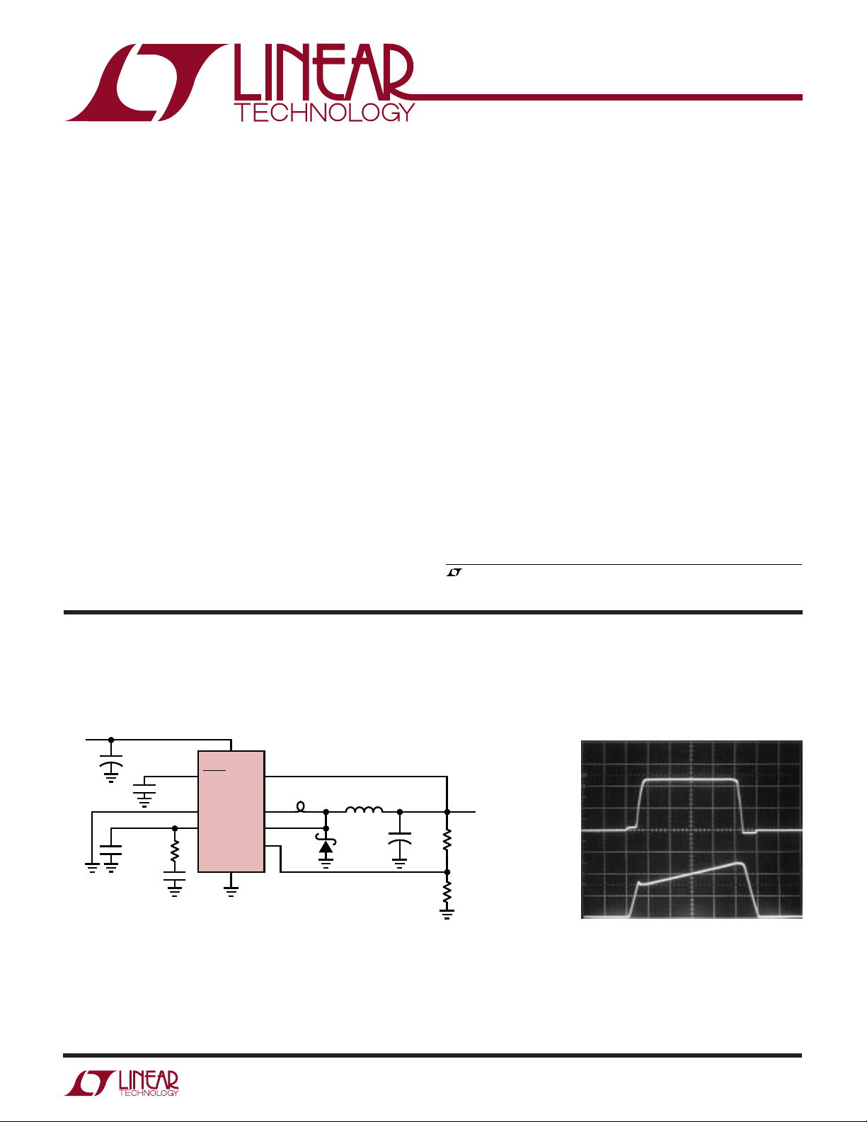
TYPICAL APPLICATIO
The LT®1777 is a Buck (step-down) regulator designed for
noise sensitive applications. It contains a dI/dt limiting
circuit programmed via a small external inductor in the
switching path. Internal circuitry also generates controlled
dV/dt ramp rates.
The monolithic die includes all oscillator, control and
protection circuitry. The part can accept operating input
voltages as high as 48V, and contains an output switch
rated at 700mA peak current. Current mode control offers
excellent dynamic input supply rejection and short-circuit
protection. The internal control circuitry is normally powered via the VCC pin, thereby minimizing power drawn
directly from the VIN supply (see Applications Information). The fused-lead SO16 package and 100kHz switching frequency allow for minimal PC board area
requirements.
, LTC and LT are registered trademarks of Linear Technology Corporation.
V
IN
24V
+
*PROGRAMS dI/dT
39µF
63V
100pF
2200pF
100pF
12k
VSW Switching WaveformsLow Noise 5V Step-Down Supply
10
V
IN
3
SHDN
LT1777
12
SYNC
14
V
C
SGND
4
V
CC
1µH*
6
V
SW
5
V
D
13
FB
7
220µH
MBRS1100
V
OUT
5V
+
100µF
10V
36.5k
1%
12.1k
1%
1777 TA01
400mA
V
SW
VOLTAGE
10V/DIV
V
SW
CURRENT
200mA/DIV
500ns/DIV
1777 TA02
1
Page 2
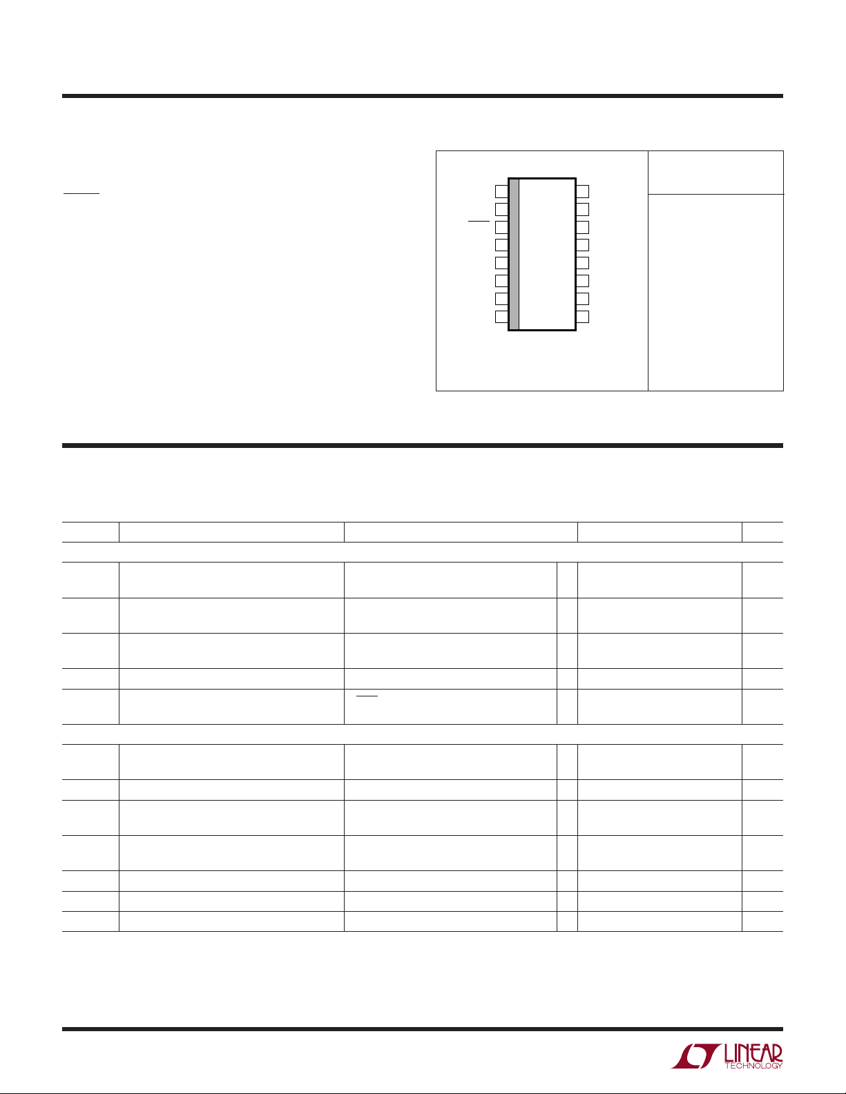
LT1777
TOP VIEW
S PACKAGE
16-LEAD PLASTIC SO
1
2
3
4
5
6
7
8
16
15
14
13
12
11
10
9
GND*
NC
SHDN
V
CC
V
D
V
SW
SGND
GND*
GND*
NC
V
C
FB
SYNC
NC
V
IN
GND*
WW
W
ABSOLUTE MAXIMUM RATINGS
U
PACKAGE
/
O
RDER I FOR ATIO
WU
(Note 1)
Supply Voltage ....................................................... 48V
Switch Voltage (VIN – VSW) (Note 4) ...................... 51V
ORDER PART
NUMBER
SHDN, SYNC Pin Voltage.......................................... 7V
VCC Pin Voltage ...................................................... 30V
FB Pin Voltage ........................................................ 3.0V
LT1777CS
LT1777IS
Operating Junction Temperature Range
LT1777C............................................... 0°C to 125°C
LT1777I ........................................... –40°C to 125°C
Storage Temperature Range ................ –65°C to 150°C
Lead Temperature (Soldering, 10 sec)................. 300°C
T
= 125°C, θJA = 50°C/W*
JMAX
Consult factory for Military grade parts.
*FOUR CORNER PINS ARE
FUSED TO INTERNAL DIE
ATTACH PADDLE FOR HEAT
SINKING. CONNECT THESE
FOUR PINS TO EXPANDED PC
LANDS FOR PROPER HEAT
SINKING.
ELECTRICAL CHARACTERISTICS
The ● denotes specifications which apply over the full operating temperature range, otherwise specifications are at TJ = 25°C.
VIN = 24V, VSW Open, VCC = 5V, VC = 1.4V unless otherwise noted.
U
SYMBOL PARAMETER CONDITIONS MIN TYP MAX UNITS
Power Supplies
V
IN(MIN)
I
VIN
I
VCC
V
VCC
Feedback Amplifier
V
REF
I
IN
g
m
I
, I
SRC
V
CL
2
Minimum Input Voltage 6.7 7.0 V
● 7.4 V
VIN Supply Current VC = 0V 620 800 µA
● 900 µA
VCC Supply Current VC = 0V 2.5 3.5 mA
● 4.5 mA
VCC Dropout Voltage (Note 2) ● 2.8 3.1 V
Shutdown Mode I
Reference Voltage 1.225 1.240 1.255 V
FB Pin Input Bias Current 600 1500 nA
Feedback Amplifier Transconductance ∆IC = ±10µA 400 650 1000 µmho
Feedback Amplifier Source or Sink Current 60 100 170 µA
SNK
Feedback Amplifier Clamp Voltage 2.0 V
Reference Voltage Line Regulation 12V ≤ VIN ≤ 48V ● 0.01 %/V
Voltage Gain 200 600 V/V
VIN
V
= 0V 30 50 µA
SHDN
● 75 µA
● 1.215 1.265 V
● 200 1500 µmho
● 45 220 µA
Page 3
LT1777
ELECTRICAL CHARACTERISTICS
The ● denotes specifications which apply over the full operating temperature range, otherwise specifications are at TJ = 25°C.
VIN = 24V, VSW Open, VCC = 5V, VC = 1.4V unless otherwise noted.
SYMBOL PARAMETER CONDITIONS MIN TYP MAX UNITS
Output Switch
R
ON
I
LIM
Current Amplifier
Timing
f Switching Frequency 90 100 110 kHz
Sync Function
SHDN Pin Function
V
SHDN
I
SHDN
Output Switch On Voltage ISW = 0.5A 1.0 1.5 V
Switch Current Limit (Note 3) ● 0.55 0.70 1.0 A
Output dl/dt Sense Voltage 1.3 V
● 0.6 2.0 V
Control Pin Threshold Duty Cycle = 0% 0.9 1.1 1.25 V
Control Voltage to Switch Transconductance 2 A/V
● 85 115 kHz
Maximum Switch Duty Cycle ● 85 90 %
Minimum Sync Amplitude ● 1.5 2.2 V
Synchronization Range ● 130 250 kHz
SYNC Pin Input R 40 kΩ
Shutdown Mode Threshold 0.5 V
● 0.2 0.8 V
Upper Lockout Threshold Switching Action On 1.260 V
Lower Lockout Threshold Switching Action Off 1.245 V
Shutdown Pin Current V
= 0V 12 20 µA
SHDN
V
= 1.25V 2.5 10 µA
SHDN
Note 1: Absolute Maximum Ratings are those values beyond which the life
of a device may be impaired.
Note 2: Control circuitry powered from V
Note 3: Switch current limit is DC trimmed and tested in production.
Inductor dI/dt rate will cause a somewhat higher current limit in actual
application.
CC
.
Note 4: During normal operation the V
below ground. However, the LT1777 may not be used in an inverting
DC/DC configuration.
pin may fly as much as 3V
SW
3
Page 4
LT1777
UW
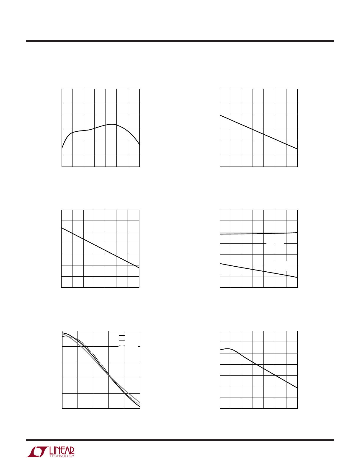
TYPICAL PERFOR A CE CHARACTERISTICS
Minimum Input Voltage
vs Temperature
7.4
7.2
7.0
6.8
6.6
INPUT VOLTAGE (V)
6.4
6.2
6.0
–50
–25 0
TEMPERATURE (°C)
Switch Current Limit
vs Duty Cycle
1000
TA = 25°C
800
600
50 100 125
25 75
1777 G01
Switch On Voltage
vs Switch Current
1.50
1.25
1.00
0.75
0.50
SWITCH VOLTAGE (V)
0.25
0
0
100 200
SWITCH CURRENT (mA)
–55°C
125°C
25°C
400 600 700
300 500
SHDN Pin Shutdown Threshold
vs Temperature
900
800
700
600
1777 G02
400
200
SWITCH CURRENT LIMIT (mA)
0
2010 30 50 70 90
0
40
DUTY CYCLE (%)
SHDN Pin Current vs Voltage
5
0
–5
–10
–15
SHDN PIN INPUT CURRENT (µA)
–20
1
0
2
SHDN PIN VOLTAGE (V)
500
400
SHDN PIN VOLTAGE (mV)
300
60
80
100
1777 G03
200
–50
–25 0
50 100 125
25 75
TEMPERATURE (°C)
1777 G04
SHDN Pin Lockout Thresholds
vs Temperature
1.30
1.28
UPPER THRESHOLD
1.26
LOWER THRESHOLD
1.24
25°C
125°C
–55°C
3
4
5
1777 G05
SHDN PIN VOLTAGE (V)
1.22
1.20
–50
–25 0
TEMPERATURE (°C)
50 100 125
25 75
1777 G06
4
Page 5
UW
TYPICAL PERFOR A CE CHARACTERISTICS
LT1777
Switching Frequency
vs Temperature
106
104
102
100
98
SWITCHING FREQUENCY (kHz)
96
94
–50 25 75
–25 0
TEMPERATURE (°C)
Output dI/dt Sense Voltage
vs Temperature
2.0
1.8
1.6
1.4
50 100 125
1777 G07
Minimum Synchronization
Voltage vs Temperature
2.25
2.00
1.75
1.50
1.25
1.00
MINIMUM SYNCHRONIZATION VOLTAGE (V)
0.75
–50 25 75
–25 0
TEMPERATURE (°C)
50 100 125
VC Pin Switching Threshold,
Clamp Voltage vs Temperature
2.2
2.0
1.8
1.6
CLAMP
VOLTAGE
1777 G08
1.2
1.0
dI/dt SENSE VOLTAGE (V)
0.8
0.6
–50 25 75
–25 0
TEMPERATURE (°C)
Feedback Amplifier Output
Current vs FB Pin Voltage
100
50
0
–50
–100
FEEDBACK AMPLIFIER OUTPUT CURRENT (µA)
–150
1.0
1.1
1.2
FB PIN VOLTAGE (V)
50 100 125
1777 G09
25°C
125°C
–55°C
1.3
1.4
1777 G11
1.5
1.4
PIN VOLTAGE (V)
C
V
1.2
1.0
0.8
–50
–25 0
TEMPERATURE (°C)
SWITCHING
THRESHOLD
50 100 125
25 75
Error Amplifier Transconductance
vs Temperature
750
700
650
600
550
500
TRANSCONDUCTANCE (µmho)
450
400
–50
–25 0
TEMPERATURE (°C)
50 100 125
25 75
1777 G10
1777 G12
5
Page 6

LT1777
PIN FUNCTIONS
UUU
GND (Pins 1, 8, 9, 16): These corner package pins are
mechanically connected to the die paddle and thus aid in
conducting away internally generated heat. As these are
electrically connected to the die substrate, they must be
held at ground potential. A direct connection to the local
ground plane is recommended.
NC (Pins 2, 11, 15): Package Pins 2, 11 and 15 are
unconnected.
SHDN (Pin 3): When pulled below the shutdown mode
threshold, nominally 0.5V, this pin turns off the regulator
and reduces VIN input current to a few tens of microamperes (shutdown mode).
When this pin is held above the shutdown mode threshold,
but below the lockout threshold, the part will be operational with the exception that output switching action will
be inhibited (lockout mode). A user-adjustable undervoltage lockout can be implemented by driving this pin from
an external resistor divider to VIN. This action is logically
“ANDed” with the internal UVLO, nominally set at 6.7V,
such that minimum VIN can be increased above 6.7V, but
not decreased (see Applications Information).
If unused, this pin should be left open. However, the high
impedance nature of this pin renders it susceptible to
coupling from the VSW node, so a small capacitor to
ground, typically 100pF or so is recommended when the
pin is left open.
VCC: (Pin 4): Pin to power the internal control circuitry
from the switching supply output. Proper use of this pin
enhances overall power supply efficiency. During start-up
conditions, internal control circuitry is powered directly
from VIN. If the output capacitor is located more than an
inch from the VCC pin, a separate 0.1µF bypass capacitor
to ground may be required right at the pin.
VD (Pin 5): This pin is used in conjunction with a small
external sense inductor to limit power path dI/dt. The
sense inductor is placed between the VSW output node and
the cathode of the freewheeling (power) diode, and the V
pin is connected to the diode. As the voltage across the
inductor reaches ±2VBE, drive to the output transistor is
D
removed or supplied accordingly to limit dI/dt (see Applications Information).
VSW (Pin 6): This is the emitter node of the output switch
and has large currents flowing through it. Keep the traces
to the switching components as short as possible to
minimize electromagnetic radiation and voltage spikes.
SGND (Pin 7): This is the device signal ground pin. The
internal reference and feedback amplifier are referred to it.
Keep the ground path connection to the FB divider and the
VC compensation capacitor free of large ground currents.
VIN (Pin 10): This is the high voltage supply pin for the
output switch. It also supplies power to the internal control
circuitry during start-up conditions or if the VCC pin is left
open. A high quality bypass capacitor which meets the
input ripple current requirements is needed here (see
Applications Information).
SYNC (Pin 12): Pin to synchronize internal oscillator to
external frequency reference. It is directly logic compatible and can be driven with any signal between 10% and
90% duty cycle. The sync function is internally disabled if
the FB pin voltage is low enough to cause oscillator
slowdown. If unused, this pin should be grounded.
FB (Pin 13): This is the inverting input to the feedback
amplifier. The noninverting input of this amplifier is internally tied to the 1.24V reference. This pin also slows down
the frequency of the internal oscillator when its voltage is
abnormally low, e.g. 2/3 of normal or less. This feature
helps maintain proper short-circuit protection. Coupling
from high speed noise to this pin can cause irregular
operation. (See Switch Node Considerations section.)
VC (Pin 14): This is the control voltage pin which is the
output of the feedback amplifier and the input of the
current comparator. Frequency compensation of the overall loop is effected by placing a capacitor (or in most cases
a series R/C combination) between this node and ground.
Coupling from high speed noise to this pin can cause
irregular operation. (See Switch Node Considerations
section.)
6
Page 7
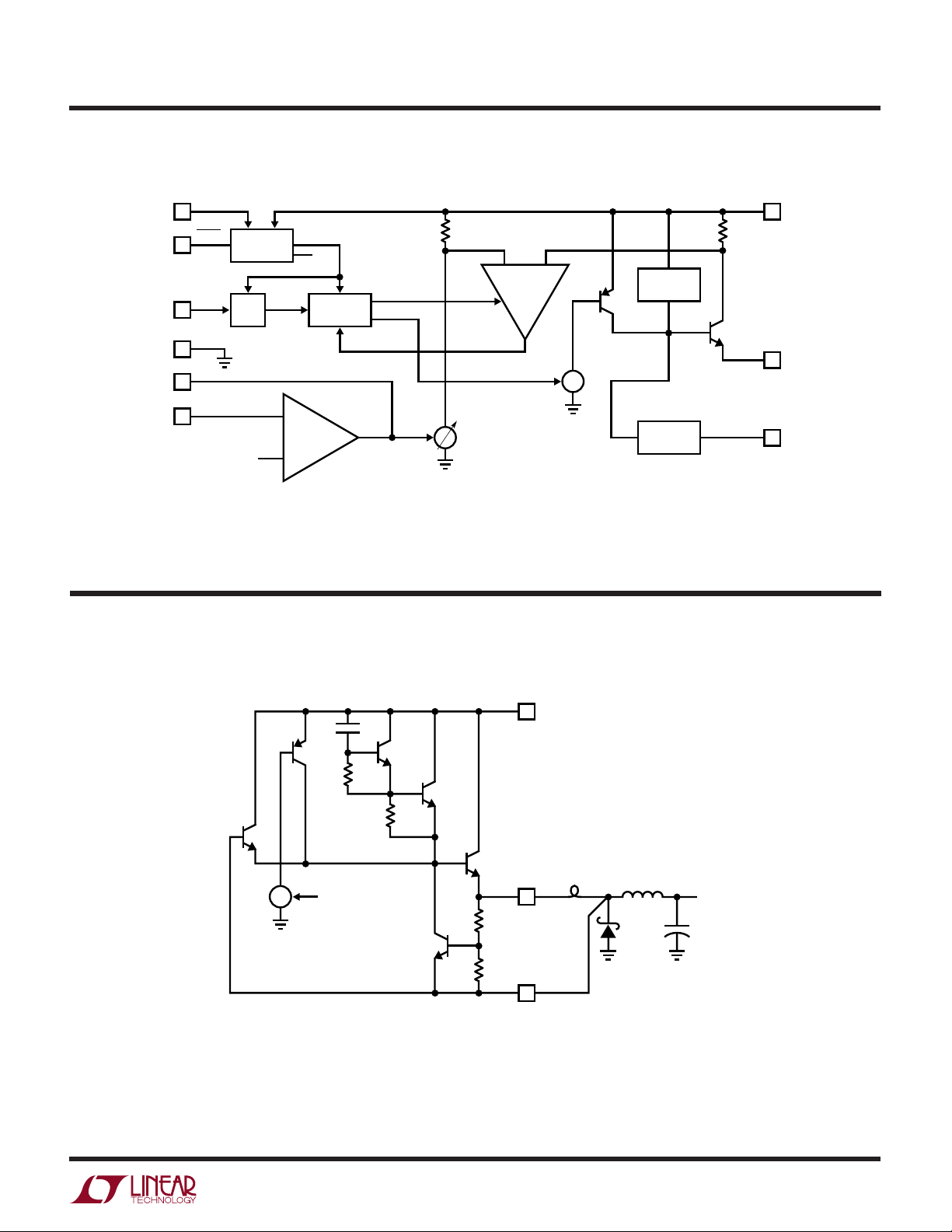
BLOCK DIAGRA
LT1777
W
V
CC
4
V
V
BG
LOGIC
FEEDBACK
AMP
g
m
B
SWDR
SWON
SHDN
3
SYNC
12
SGND
7
V
C
14
FB
13
OSC
V
BG
BIAS
R1
I
I
2
WW
OUTPUT STAGE SI PLIFIED SCHE ATIC
I
COMP
V
IN
10
R
SENSE
–dV/dt
LIMITER
Q2
Q1
V
SW
6
I
1
I
V
±dI/dt
LIMITER
1777 BD
D
5
V
C1
Q3Q2
R1
Q4
R2
Q6
Q1
I
1
SWITCH ON
I
SIGNAL
R3
Q5
R4
IN
L
V
SW
SENSE
L
MAIN
V
OUT
+
V
D
1777 SS
NOTE: R3 = R4
7
Page 8

LT1777
OPERATIO
U
The LT1777 is a current mode step-down switcher regulator IC designed for low noise operation. The Block
Diagram shows an overall view of the system. The individual blocks are straightforward and similar to those
found in traditional designs, including: Internal Bias Regulator, Oscillator, Logic, and Feedback Amplifier. The novel
portion includes a specialized Output Switch section including circuits to limit the dI/dt and dV/dt switching rates.
The LT1777 operates much the same as traditional current
mode switchers, the major difference being its specialized
output switch section. Due to space constraints, this
discussion will not reiterate the basics of current mode
switcher/controllers and the “buck” topology. A good
source of information on these topics is Application Note
AN19.
A straightforward output stage is provided by current
source I1 driving the base of PNP transistor Q2. The
collector of Q2 in turn drives the base of NPN output device
Q1. The considerable base/collector capacitance of PNP
Q2 acts to limit dV/dt rate during switch turn-on. However,
when the switch is to be turned off, the only natural limit
to voltage slew rate would be the collector/base capacitance of Q1 providing drive for the same device. While
dependent upon output load level and Q1’s β, the turn-off
voltage slew rate would be typically much faster than the
turn-on rate. To limit the voltage slew rate on switch turnoff, an extra function is supplied. This is denoted by the
block labeled “–dV/dt Limiter.”
The details of the – dV/dt Limiter can be seen in the Output
Stage Simplified Schematic. Transistors Q3 and Q4 are
connected in a Darlington configuration whose input is
coupled with small-valued capacitor C1 to the VIN supply
rail. The product of negative voltage slew rate times this
capacitor value equals current, and when this current
through emitter/base resistor R1 exceeds a diode drop, Q3
and then Q4 turn on supplying base drive to output device
Q1 to limit –dV/dt rate.
In addition to voltage rates, the current slew rate also
needs to be controlled for reduced noise behavior. This is
provided by the section in the Block Diagram labeled
“±dI/dt Limiter.” The details of this circuit can be seen in
the Output Stage Simplified Schematic. Note that an extra,
small-valued inductor, termed the “sense inductor” has
been added to the classic buck topology. As this inductor
is external to the LT1777, its value can be chosen by the
user allowing for optimization on a per application basis.
Operation of the current slew limiter is as follows: The
product of the sense inductor times the dI/dt through it
generates a voltage according to the well known formula
V = (L)(dI/dt). The remainder of the circuit is configured
such that when the voltage across the sense inductor
reaches ±2VBE, drive current will be supplied or removed
as necessary to limit current slew rate. The actual sensing
is performed between the output node labeled VSW and a
new node labeled VD.
In the case of switch turn-on, current drive is provided by
PNP Q2. If the voltage at VSW reaches 2VBE above that at
VD, transistor Q5 turns on and removes a portion of Q2’s
drive from Q1’s base. Similarly for turn-off, as the V
node goes 2VBE below VD, transistor Q6 then turns on to
drive Q1’s base as needed. The net effect is that of limiting
the switch node dI/dt in both directions at a rate inversely
proportional to the external sense inductor value.
SW
8
Page 9

LT1777
+
+
LT1777
V
IN
C1
D1
V
OUT
1777 F01
C2
L
SENSE
L
MAIN
U
WUU
APPLICATIONS INFORMATION
Basics of Low Noise Operation
Switching power supply circuits are often preferred over
linear topologies for their improved efficiency (P
However, their typically rapid voltage and current slew
rates often cause “radio frequency” interference problems, commonly referred to as “RFI”. The LT1777 is
designed to provide a less aggressive voltage slew rate
and a user-programmable current slew rate to eliminate
the highest frequency harmonics of RFI emissions. These
highest frequency components are typically the most
troublesome. Optimum behavior is obtained by a combination of proper circuit design, which includes passive
component selection, and proper printed circuit board
layout technique.
There are two types of RFI emissions, i.e.,
radiated
. Conducted interference travels directly through
conducted
“wires”, as opposed to radiated interference, which travels
through the air. Conducted RFI can be created by a
switching power supply at its input voltage supply node,
its output node(s) or both. It is typically caused by pulsatile
current flow through the residual high frequency impedance (ESR) of bypass capacitors.
Radiated interference can be of two types: electric (E field)
or magnetic (B field). E field interference is caused by stray
capacitance coupling of the node(s) which swing rapidly
over a large voltage excursion. In the LT1777, this includes the VSW and VD nodes. E field radiation is kept low
by minimizing the length and area of all traces connected
to these nodes. A ground plane should always be used
under the switcher circuitry to prevent interplane coupling. Although these nodes swing over a voltage range
roughly equal to the input voltage, the limited dV/dt rate of
the LT1777 reduces the highest frequency components of
the generated E field RFI.
OUT
/ PIN).
and
external sense inductor to set a maximum allowed dI/dt
rate. This attenuates the highest frequency components of
generated B field RFI. Minimal lead length in the path is
also essential to minimize generated RFI.
A second potential source of magnetic RFI is the main
(power) inductor. Fortunately, the natural triangular behavior of the current waveform in the main inductor tends
to generate magnetic field energy concentrated in the
fundamental and lower harmonics. Nevertheless, the relatively intense magnetic field present in the main inductor
can cause coupling problems, especially if the main inductor is of an open construction type. So called rod or barrel
inductors may be the physically smallest and most effective types, but their magnetic field extends far beyond the
device itself. Closed type inductors, toroids for example,
contain the magnetic field nearly completely. These are
generally preferred for low noise behavior.
The sense inductor sees a much more rapid current slew
rate than does the main inductor. However the sense
inductor is physically smaller and of much lower inductance than the main inductor. These factors tend to reduce
its propensity to generate magnetic interference problems. Nevertheless, more sensitive applications can opt
for a closed type magnetic construction on the sense
inductor.
Figure 1. High Speed Current Switching Paths
B field RFI is simply coupling of high frequency magnetic
fields generated by the offending circuitry. High frequency
magnetic fields are created by relatively rapidly changing
currents, and the high speed current switching path in the
LT1777 is shown schematically in Figure 1. This includes
the input capacitor, output switch, sense inductor and
output diode. Normal switching supply operation requires
a rapid switching of current back and forth between the
output switch and output diode. The LT1777 uses the
Selecting Sense Inductor
The LT1777 uses an external sense inductor to set a
theoretical limit for current ramp rate according to the
formula:
V
2
L
SENSE
BE
Max dI dt
/ =
9
Page 10

LT1777
U
WUU
APPLICATIONS INFORMATION
Deciding upon a value for the sense inductor involves
evaluating the trade-off between overall efficiency (P
PIN) and switch current slew rate. Larger sense inductors
yield lower current slew rates which offer reduced high
frequency RFI emissions, but at the expense of poorer
efficiency.
The question is “What is the allowed range of values for a
sense inductor in a given application?” There is really no
minimum
limit to the sense inductor, i.e., its value is
allowed to be zero. (In other words, the physical sense
inductor ceases to exist and is replaced by a short circuit.)
This will yield the highest efficiency possible in a given
situation. Although an explicit current slew rate no longer
exists, the naturally less aggressive nature of the LT1777
will often yield quieter supply operation than other standard switching regulators.
As far as the
maximum
allowable value for the sense
inductor, this is dictated by the current ramp rate in the
main inductor during the conventional part of the switching cycle. It is generally overconservative to limit the
switch current slew rate to that exhibited by the main
inductor. This would potentially yield a triangular current
waveform. Efficiency would be greatly reduced at little
further gain in noise performance. Stated mathematically,
maximum slew rate in the main inductor occurs at maximum input voltage as:
OUT
/
As an example, a maximum input voltage of 36V, an output
voltage of 5V and a main inductor value of 220µH yields a
maximum suggested sense inductor value of 3.5µH.
Circuit behavior versus sense inductor value is shown in
the oscilloscope photos in Figure 2. The circuit and operating conditions are similar to the Typical Application on
the first page of this data sheet with the exception that the
sense inductor is allowed to assume the series of values:
0µH, 0.47µH, 1µH and 2.2µH. Figure 2a shows a close-up
of the leading edge (turn-on) of the current waveform.
Values of 0µH and 0.47µH are found to yield a dI/dt of
about 2.2A/µs, while 1µH yields 1.4A/µs and 2.2µH yields
0.6A/µs. Figure 2b shows the trailing edge (turn-off) of the
100mA/DIV
200ns/DIV
(a) Leading Edge
1777 F02a
Max V V
dI
=
dt
–
IN OUT
L
MAIN
The sense inductor experiences 2VBE of applied voltage.
This is perhaps 1.0V at a maximum hot condition. If we use
an additional factor of two to be conservative, this yields
a maximum sense inductor value as follows:
L
=
–
IN OUT
MAIN
Max V V
,
or
.
V
–
IN OUT
0505.
L
SENSE
Max L L
Max V V
V
=
SENSE MAIN
10
100mA/DIV
200ns/DIV
(b) Trailing Edge
Figure 2. VSW Node Current Behavior vs L
L
= 0µH, 0.47µH, 1.0µH and 2.2µH
SENSE
1777 F02b
SENSE
Value.
Page 11

LT1777
U
WUU
APPLICATIONS INFORMATION
current waveform. The four sense inductor values of 0µH,
0.47µH, 1µH and 2.2µH yield dI/dt rates of roughly
4.5A/µs, 2.2A/µs, 1.4A/µs and 0.6A/µs, respectively.
These photos show that there is a minimum effective value
for sense inductance, which is 0.47µH for a typical part at
room temperature as shown. This value inductor has a
small effect on the trailing edge rate, but essentially no
effect on the rising edge. Minimum effective sense inductance value means that inductors much smaller than this
value will have substantially the same performance as zero
inductance, such that these inductors serve no useful
purpose.
In summary,
1. The LT1777 uses an external sense inductor to set a
theoretical limit for current ramp rate according to the
formula:
V
2
L
=
BE
SENSE
05.
Max V V
IN OUT
V
–
Max dI dt
/ =
2. Allowable range for the sense inductor runs from a
minimum of 0 to a maximum of:
Max L L
SENSE MAIN
3. The minimum effective inductor size is typically 0.47µH.
Harmonic Behavior
The LT1676 is a high efficiency “cousin” to the LT1777. An
additional set of oscilloscope photographs in Figure 3
show the leading edge and trailing edge of the current
waveform when this part is substituted for the LT1777.
(No sense inductor is used with the LT1676.) The leading
and trailing edges of the LT1676 current waveform are
much faster than that of the LT1777, even when the
LT1777 uses a sense inductor of 0µH. The 10% to 90%
rise time/fall time is on the order of 10ns to 20ns, too fast
to measure accurately at the horizontal sweep rate of
200ns/DIV.
While this time-based analysis demonstrates that the
current waveform of the LT1777 is quieter than standard
high efficiency buck converters, some users may prefer to
see a direct comparison on a frequency domain basis.
Figures 4a, 4b, and 4c show a spectral analysis of the
current waveforms. The horizontal axis is 2MHz/DIV (0MHz
to 20MHz), and the vertical axis is 10dB/DIV. All photos
were taken with VIN = 24V and V
= 5V at 400mA. Figure
OUT
4a is of the LT1676 and is for comparison purposes.
Figures 4b and 4c are of the LT1777 with a sense inductor
of 0µH and 2.2µH, respectively. A decrease in high fre-
quency energy is seen when going from the LT1676 to the
LT1777 with no sense inductor, and a further improvement with a 2.2µH sense inductor. For example, at 10MHz,
the LT1777 shows an improvement of about –10dB with
0µH and perhaps –25dB with 2.2µH.
100mA/DIV
200ns/DIV
(a) Leading Edge
Figure 3. LT1676 Current Behavior for Comparison Purposes Only
1777 F03a
100mA/DIV
200ns/DIV
(b) Trailing Edge
1777 F03b
11
Page 12

LT1777
U
WUU
APPLICATIONS INFORMATION
10dB/DIV
0MHz to 20MHz (2MHz/DIV)
(a) LT1676 for Comparison
10dB/DIV
1777 F04a
voltage of 12V, and then 36V. Once again the circuit is the
Typical Application shown on the first page of this data
sheet, with an output load of 400mA.
Figure 5a, with VIN of 12V, shows a relatively rectangular
voltage waveform. The limited voltage slew rate still allows
for nearly vertical switching edges, so little power is
wasted. A positive-going step before the leading edge and
a negative-going step after the trailing edge can be seen.
These are evidence of the internal current limiting circuitry
at work.
Figure 5b, with VIN of 36V, shows a substantially
nonrectangular waveform. The limited voltage slew rate is
clearly evident as transitions take a few hundred nanoseconds. Efficiency (P
OUT/PIN
) is reduced as a result of the
slower transitions. For comparison purposes, the oscilloscope photo in Figure 6 shows the performance of the high
efficiency LT1676. Voltage transitions are well under
100ns and the waveform appears quite rectangular.
0MHz to 20MHz (2MHz/DIV)
(b) LT1777 with L
10dB/DIV
0MHz to 20MHz (2MHz/DIV)
(c) LT1777 with L
Figure 4. Spectral Analysis of Current Waveforms in
Figures 2 and 3. (VIN = 24V, V
SENSE
SENSE
OUT
= 0µH
= 2.2µH
= 5V, I
1777 F04b
1777 F04c
= 400mA)
OUT
Voltage Waveform Behavior
Unlike current behavior, voltage slew rate of the LT1777 is
not adjustable by the user. No component selection or
other action is required. Nevertheless, it is instructive to
examine typical behavior. The oscilloscope photos in
Figure 5 show the VSW voltage waveform with an input
2V/DIV
GND
1µs/DIV
(a) VIN = 12V
10V/DIV
GND
500ns/DIV
(b) VIN = 36V
Figure 5. VSW Node Voltage Behavior
1777 F05a
1777 F05b
12
Page 13

LT1777
U
WUU
APPLICATIONS INFORMATION
10V/DIV
GND
500ns/DIV
Figure 6. LT1676 VSW Node Voltage Behavior
for Comparison Purposes Only, VIN = 36V
Selecting Main Inductor
There are several parameters to consider when selecting
a main inductor. These include inductance value, peak
current rating (to avoid core saturation), DC resistance,
construction type, physical size, and of course, cost.
Once the inductance value is decided, inductor peak
current rating and resistance need to be considered. Here,
the inductor peak current rating refers to the onset of
saturation in the core material, although manufacturers
sometimes specify a “peak current rating” which is derived from a worst-case combination of core saturation
and self-heating effects. Inductor winding resistance alone
limits the inductor’s current carrying capability as the I2R
power threatens to overheat the inductor. Remember to
include the condition of output short circuit, if applicable.
Although the peak current rating of the inductor can be
exceeded in short-circuit operation, as core saturation per
se is not destructive to the core, excess resistive selfheating is still a potential problem.
The final inductor selection is generally based on cost,
which usually translates into choosing the smallest physical size part which meets the desired inductance value,
resistance and current carrying capability. An additional
factor to consider is that of physical construction. Briefly
stated, “open” inductors built on a rod- or barrel-shaped
core generally offer the smallest physical size and lowest
cost. However their open construction does not contain
the resulting magnetic field, and they may not be acceptable in RFI-sensitive applications. (A mitigating factor is
that, as mentioned previously, the AC current passing
1777 F06
through the main inductor has most of its energy concentrated in the fundamental and lower harmonics.) Toroidal
style inductors, many available in surface mount configuration, offer a reduced external magnetic field, generally at
an increase in cost and physical size. Although custom
design is always a possibility, most potential LT1777 applications can be handled by the array of standard, off-theshelf inductor products offered by the major suppliers.
Selecting Bypass Capacitors
The basic topology as shown in the Typical Application on
the first page uses two bypass capacitors, one for the V
input supply and one for the V
User selection of an appropriate output capacitor is relatively easy, as this capacitor sees only the AC ripple current
in the inductor L1. As the LT1777 is designed for buck or
step-down applications, output voltage will nearly always
be compatible with tantalum type capacitors, which are
generally available in ratings up to 35V or so. These
tantalum types offer good volumetric efficiency, and many
are available with specified ESR performance. The product
of inductor AC ripple current and output capacitor ESR will
manifest itself as peak-to-peak voltage ripple on the output
node. (Note: If this ripple becomes too large, heavier
control loop compensation, at least at the switching frequency, may be required on the VC pin.)
The input bypass capacitor can present a more difficult
choice. In a typical application e.g., 24VIN to 5V
relatively heavy VIN current is drawn by the power switch
for only a small portion of the oscillator period (low ON
duty cycle). The resulting RMS ripple current, for which
the capacitor must be rated, can be several times the DC
average VIN current. The straightforward choice for a low
volume, surface mountable electrolytic capacitor with
good ESR/ripple current ratings is a tantalum type. However, worst-case (high) input voltage coupled with standard capacitor voltage derating may exceed the 35V or so
for which tantalum capacitors are generally available.
Relatively bulky “high frequency” aluminum electrolytic
types, specifically constructed and rated for switching
supply applications, may then be the only choice.
Additionally, it may be advantageous to parallel the input
and output capacitors with 0.1µF ceramic bypass capaci-
output supply.
OUT
OUT
IN
,
13
Page 14

LT1777
FB DIVIDER THEVENIN VOLTAGE (V)
0
0
f
OSC
(kHz)
20
40
60
80
100
120
0.25 0.50 0.75 1.00
1777 F07
1.25
R
TH
LT1777
FB
RTH = 10k RTH = 4.7k
R
TH
= 22k
U
WUU
APPLICATIONS INFORMATION
tors. Their relatively low ESR in the mid-MHz region can
further attenuate high speed glitches.
Maximum Load/Short-Circuit Considerations
The LT1777 is a current mode controller. It uses the V
node voltage as an input to a current comparator, which
turns off the output switch on a cycle-by-cycle basis as
this peak current is reached. The internal clamp on the V
node, nominally 2.0V, then acts as an output switch peak
current limit. This action becomes the switch current limit
specification. The maximum available output power is
then determined by the switch current limit.
A potential controllability problem could occur under
short-circuit conditions. If the power supply output is
short circuited, the feedback amplifier responds to the low
output voltage by raising the control voltage, VC, to its
peak current limit value. Ideally, the output switch would
be turned on, and then turned off as its current exceeded
the value indicated by VC. However, there is finite response
time involved in both the current comparator and turn-off
of the output switch. These result in a minimum on time
t
ON(MIN)
. When combined with the large ratio of VIN to
(VF + I • R), the diode forward voltage plus inductor I • R
voltage drop, the potential exists for a loss of control.
Expressed mathematically the requirement to maintain
control is:
C
C
The solution to this dilemma is to slow down the oscillator
when the FB pin voltage is abnormally low thereby indicating some sort of short-circuit condition. Figure 7 shows
the typical response of oscillator frequency vs FB pin
voltage. Oscillator frequency is normal until FB voltage
drops to about half of its normal value. Below this point the
oscillator frequency decreases linearly down to a limit of
about 25kHz. This lower oscillator frequency during shortcircuit conditions can then maintain control with the
effective minimum on time.
A further potential problem with short-circuit operation
might occur if the user were operating the part with its
oscillator slaved to an external frequency source via the
SYNC pin. However, the LT1777 has circuitry to automatically disable the sync function when the oscillator is
slowed down due to abnormally low FB voltage.
ft
()( )
where:
f = switching frequency
tON = switch on time
VF = diode forward voltage
VIN = Input voltage
I • R = inductor I • R voltage drop
If this condition is not observed, the current will not be
limited at IPK, but will cycle-by-cycle ratchet up to some
higher value. Using the nominal LT1777 clock frequency
of 100kHz, a VIN of 48V and a (VF + I • R) of say, 0.7V, the
maximum tON to maintain control would be approximately
140ns, an unacceptably short time.
14
ON
VIR
+ •
F
≤
V
IN
Figure 7. Oscillator Frequency vs FB Divider
Thevenin Voltage and Impedance
Feedback Divider Considerations
An LT1777 application typically includes a resistive divider
between V
the FB pin to the reference voltage V
and ground, the center node of which drives
OUT
. This establishes
REF
a fixed ratio between the two resistors, but a second
degree of freedom is offered by the overall impedance
level of the resistor pair. The most obvious effect this has
is one of efficiency—a higher resistance feedback divider
will waste less power and offer somewhat higher efficiency, especially at light load.
Page 15

LT1777
U
WUU
APPLICATIONS INFORMATION
However, remember that oscillator slowdown to achieve
short-circuit protection (discussed above) is dependent
on FB pin behavior, and this in turn, is sensitive to FB node
external impedance. The graph in Figure 7 shows the
typical relationship between FB pin voltage, driving impedance and oscillator frequency. This shows that as
feedback network impedance increases beyond 10k, complete oscillator slowdown is not achieved, and shortcircuit protection may be compromised. And as a practical
matter, the product of FB pin bias current and larger FB
network impedances will cause increasing output voltage
error. (Nominal cancellation for 10k of FB Thevenin impedance is included internally.)
Thermal Considerations
Care should be taken to ensure that the worst-case input
voltage and load current conditions do not cause excessive die temperatures. The SO16 package is rated at
50°C/W when the four corner package pins are connected
to a good ground plane. (These corner pins are internally
fused to the die paddle for improved thermal performance.) Die junction temperature is then a function of
ambient temperature and internal dissipation as follows:
TJ = TA + θ
Total internally dissipated power is composed of three
parts, quiescent power, DC switch loss and AC switch
loss. The AC switch loss will often dominate the total
dissipation, and this is unfortunately difficult to estimate
accurately.
Two options are suggested to the potential user. The first
is to observe the graphical data presented in the Typical
Applications section. Internal LT1777 dissipation vs load
current is given for output voltages of 5V and 3.3V, with
input voltages of 12V, 24V and 36V, and with sense
inductors of 0µH, 1µH, and 2.2µH (Figures 9 and 11).
While it is true that the user’s ultimate circuit may use
somewhat different passive components than the examples given, it turns out that internal IC dissipation is not
very sensitive to these changes.
In cases where the user’s potential circuit differs significantly from the examples given, an empirical method is
JA
• P
INT
suggested. Operate the proposed power supply over the
applicable input voltage and load current ranges. Measure
the input power and output power, and calculate the
difference as “lost power.” This measured lost power
minus estimated inductor and diode dissipation yields a
figure for internal LT1777 dissipation. Fortunately, as
LT1777 internal dissipation dominates total lost power,
inductor and diode power need not be estimated very
accurately. Inductor power may be estimated as I2R where
I is the load current and R is the DC resistance of the
inductor. (Loss in the sense inductor is usually so small
that only the main inductor must be considered.) Diode
power may be estimated as 1/2 • VF • I • DC, where VF is the
diode forward voltage, I is the load current and DC is the
duty cycle percentage when the diode is conducting.
Frequency Compensation
Loop frequency compensation is performed by connecting a capacitor, or in most cases a series R/C, from the
output of the error amplifier (VC pin) to ground. Proper
loop compensation may be obtained by empirical methods as described in detail in Application Note AN19.
Briefly, this involves applying a load transient and observing the dynamic response over the expected range of V
and I
As a practical matter, a second small capacitor, directly
from the VC pin to ground is generally recommended to
attenuate capacitive coupling from the VSW and VD pins. A
typical value for this capacitor is 100pF. (See Switch Node
Considerations).
Switch Node Considerations
In spite of the fact that the LT1777 is a low noise converter,
it is still possible for the part to cause problems by
“coupling to itself.” Specifically, this can occur if the V
pin is allowed to capacitively couple in an uncontrolled
manner to the part’s high impedance nodes, i.e., SHDN,
SYNC, VC and FB. This can cause erratic operation such as
odd/even cycle behavior, pulse width “nervousness”, improper output voltage and/or premature current limit
action.
LOAD
values.
IN
SW
15
Page 16

LT1777
U
WUU
APPLICATIONS INFORMATION
As an example, assume that the capacitance between the
VSW node and a high impedance pin node is 0.1pF, and that
the high impedance node in question exhibits a capacitance of 1pF to ground. Also assume a “typical” 36VIN to
5V
application. Due to the large voltage excursion at
OUT
the VSW node, this will couple a 3.5V(!) transient to the
high impedance pin, causing abnormal operation. An
explicit 100pF capacitor added to the node will reduce the
amplitude of the disturbance to more like 35mV (although
settling
time
will increase).
Specific pin recommendations are as follows:
SHDN: If unused, add a 100pF capacitor to ground.
SYNC: Ground if unused.
VC: Add a capacitor directly to ground in addition to the
explicit compensation network. A value of one-tenth of
the main compensation capacitor is recommended, up
to a maximum of 100pF.
FB: Assuming the VC pin is handled properly, this pin
usually requires no explicit capacitor of its own, but
keep this node physically small to minimize stray
capacitance.
16
Page 17

U
TYPICAL APPLICATIONS
LT1777
Basic 5V Output Application
Figure 8 shows a basic application that produces 5V at up
to 500mA I
. Efficiency and Internal Power Dissipation
OUT
graphs are shown in Figure 9 for input voltages of 12V,
24V and 36V, and for sense inductor values of 0µH, 1µH
and 2.2µH. Be aware that continuous operation at the
combination of high input voltage, large sense inductor
and high output current may not be possible due to
thermal constraints. (Brief transients in input voltage or
V
10V TO 40V
IN
+
C1
39µF
63V
C1: PANASONIC HFQ ELECTROLYTIC
C2: AVX D CASE TPSD107M010R0080
C3, C4, C5: NPO OR X7R
C6, C7: Z5U
D1: MOTOROLA 100V, 1A SMD SCHOTTKY
MBRS1100
C6
0.1µF
C4
100pF
C5
100pF
R3
12k
C3
2200pF
3
12
14
10
V
IN
V
SHDN
SYNC
V
CC
LT1777
V
SW
V
C
D
FB
SGND
7
L1: SENSE INDUCTOR CAN VARY FROM 0µH TO 2.2µH
AS PER APPLICATION. GRAPHICAL DATA TAKEN WITH:
1µH = D01608C-102, COILCRAFT OR SIMILAR
2.2µH = D01608C-222, COILCRAFT OR SIMILAR (SEE TEXT)
L2: COILCRAFT D03316-224 OR SIMILAR (SEE TEXT)
output current should not present a problem, though.) As
shown, the SHDN and SYNC pins are unused, however
either (or both) can be optionally driven by external signals
as desired.
The data as shown were performed using an off-the-shelf
Coilcraft DO3316-224 as the main inductor. This is a
cost-effective inductor using an open style of construction. For a toroidal style inductor, the Coiltronics
CTX250-4 or similar may be substituted.
4
L1
0µH TO 2.2µH
(SEE BELOW)
6
5
13
220µH
D1
L2
V
OUT
+
C2
100µF
10V
C7
0.1µF
R1
36.5k
1%
R2
12.1k
1%
1777 F08
5V
Figure 8. Basic 5V Output Application
17
Page 18

LT1777
I
OUT
(mA)
0
0.6
0.4
0.2
1.4
1.2
1.0
0.8
1777 F09b
INTERNAL DISSIPATION (W)
10
1000
100
1µH
0µH
L
SENSE
=
2.2µH
VIN = 12V
V
OUT
= 5V
T
A
= 25°C
I
OUT
(mA)
0
0.6
0.4
0.2
1.4
1.2
1.0
0.8
1777 F09d
INTERNAL DISSIPATION (W)
10
1000
100
1µH
0µH
L
SENSE
=
2.2µH
VIN = 24V
V
OUT
= 5V
T
A
= 25°C
I
OUT
(mA)
0
0.6
0.4
0.2
1.4
1.2
1.0
0.8
1777 F09f
INTERNAL DISSIPATION (W)
10
1000
100
1µH
0µH
L
SENSE
=
2.2µH
VIN = 36V
V
OUT
= 5V
T
A
= 25°C
U
TYPICAL APPLICATIONS
VIN = 12V
VIN = 24V
90
VIN = 12V
V
OUT
80
= 25°C
T
A
70
60
50
EFFICIENCY (%)
40
30
20
1
90
VIN = 24V
V
OUT
80
T
= 25°C
A
70
60
50
EFFICIENCY (%)
40
Efficiency
= 5V
10 100 1000
I
(mA)
LOAD
= 5V
L
L
SENSE
SENSE
0µH
0µH
Internal Dissipation
=
1µH
2.2µH
1777 F09a
=
1µH
2.2µH
VIN = 36V
30
20
90
80
70
60
50
EFFICIENCY (%)
40
30
20
1
1
VIN = 36V
V
OUT
= 25°C
T
A
Figure 9. Efficiency and LT1777 Internal Dissipation for the Basic 5V Output Application
10 100 1000
I
(mA)
LOAD
= 5V
10 100 1000
I
(mA)
LOAD
L
SENSE
0µH
1777 F09c
=
1µH
2.2µH
1777 F09e
18
Page 19

U
TYPICAL APPLICATIONS
LT1777
Basic 3.3V Output Application
Figure 10 shows a circuit similar to the previous example,
but modified for a 3.3V output. Once again, Efficiency and
Internal Power Dissipation graphs are shown in Figure 11
for input voltages of 12V, 24V and 36V, and for sense
inductor values of 0µH, 1µH and 2.2µH. It is interesting to
note that internal LT1777 dissipation is very close to the
5V example. This confirms the fact that internal LT1777
V
10V TO 40V
IN
+
C1
39µF
63V
C1: PANASONIC HFQ ELECTROLYTIC
C2: AVX D CASE TPSD107M010R0080
C3, C4, C5: NPO OR X7R
C6, C7: Z5U
D1: MOTOROLA 100V, 1A SMD SCHOTTKY
MBRS1100
C4
100pF
C6
0.1µF
C5
100pF
R3
12k
C3
2200pF
3
12
14
10
V
IN
V
SHDN
SYNC
V
CC
LT1777
V
SW
V
C
D
FB
SGND
7
L1: SENSE INDUCTOR CAN VARY FROM 0µH TO 2.2µH
AS PER APPLICATION. GRAPHICAL DATA TAKEN WITH:
1µH = D01608C-102, COILCRAFT OR SIMILAR
2.2µH = D01608C-222, COILCRAFT OR SIMILAR (SEE TEXT)
L2: COILCRAFT D03316-154 OR SIMILAR (SEE TEXT)
dissipation is largely determined by input voltage, load
current and sense inductor, and is only a weak function of
output voltage.
The data as shown were performed using an off-the-shelf
Coilcraft DO3316-154 as the main inductor. This is a costeffective inductor using an open style of construction. For
a toroidal style inductor, the Coiltronics CTX150-4 or
similar may be substituted.
4
L1
0µH TO 2.2µH
(SEE BELOW)
6
5
13
L2
150µH
D1
V
OUT
+
C2
100µF
10V
C7
0.1µF
R1
20k
1%
R2
12.1k
1%
1777 F10
3.3V
Figure 10. Basic 3.3V Output Application
19
Page 20

LT1777
I
OUT
(mA)
0
0.6
0.4
0.2
1.4
1.2
1.0
0.8
1777 F11b
INTERNAL DISSIPATION (W)
10
1000
100
1µH
0µH
L
SENSE
=
2.2µH
VIN = 12V
V
OUT
= 3.3V
T
A
= 25°C
I
OUT
(mA)
0
0.6
0.4
0.2
1.4
1.2
1.0
0.8
1777 F11d
INTERNAL DISSIPATION (W)
10
1000
100
1µH
0µH
L
SENSE
=
2.2µH
VIN = 24V
V
OUT
= 3.3V
T
A
= 25°C
I
OUT
(mA)
0
0.6
0.4
0.2
1.4
1.2
1.0
0.8
1777 F11f
INTERNAL DISSIPATION (W)
10
1000
100
1µH
0µH
L
SENSE
=
2.2µH
VIN = 36V
V
OUT
= 3.3V
T
A
= 25°C
U
TYPICAL APPLICATIONS
VIN = 12V
VIN = 24V
90
VIN = 12V
V
OUT
80
= 25°C
T
A
70
60
50
EFFICIENCY (%)
40
30
20
1
90
VIN = 24V
V
OUT
80
= 25°C
T
A
70
60
50
EFFICIENCY (%)
40
Efficiency
= 3.3V
10 100 1000
I
(mA)
LOAD
= 3.3V
L
SENSE
L
SENSE
0µH
0µH
Internal Dissipation
=
1µH
2.2µH
1777 F11a
=
1µH
2.2µH
VIN = 36V
30
20
1
90
80
70
60
50
EFFICIENCY (%)
40
30
20
1
10 100 1000
I
(mA)
LOAD
VIN = 36V
= 3.3V
V
OUT
= 25°C
T
A
10 100 1000
I
(mA)
LOAD
Figure 11. Efficiency and LT1777 Internal Dissipation for the Basic 3.3V Output Application
L
SENSE
0µH
1777 F11c
=
1µH
2.2µH
1777 F11e
20
Page 21

U
TYPICAL APPLICATIONS
LT1777
Optional Input/Output Filtering
When minimum
conducted
noise is required, it is often
advantageous to add an explicit input and/or output filter
to the topology. This can be a cost-effective way to reduce
conducted noise on the input or output node by an order
of magnitude or more. The exact details involved are a bit
lengthy, so the user is referred to the thorough treatments
in Application Notes AN19 and AN44. However, an example will be given to illustrate the principles involved.
Figure 12 shows the previous “Basic 5V Output Application” modified with an additional input inductor and an
output L/C combination. The dramatic improvement in
noise performance is seen in the accompanying oscilloscope photos shown in Figures 13 and 14. Operating
conditions are VIN = 24V, I
= 400mA. The pair of scope
OUT
photos in Figure 13 show the response at the input node,
before and after the additional 33µH inductor is added. The
upper waveform shows an AC-coupled version of the
L3
33µH
V
IN
+
3
12
14
Figure 12. Basic 5V Application with Optional Input/Output Filters
SHDN
SYNC
V
C
V
IN
LT1777
SGND
10
4
V
CC
6
V
SW
5
V
D
13
FB
7
output voltage at 50mV/DIV, and the lower waveform is a
DC-coupled representation of current into the node at
50mA/DIV. Input voltage ripple is seen to decrease from
100mV
to perhaps 10mV
P-P
. Ripple current is also seen
P-P
to decrease dramatically. (This improvement in AC ripple
current actually affects
radiated
magnetic noise.)
The next pair of scope photos in Figure 14 show an
AC-coupled version of the output node at 2mV/DIV.
Voltage ripple is seen to be originally about 12mV
P-P
, with
most of the energy in the lowest harmonics. After the
addition of a 4.7µH inductor and a second 100µF output
capacitor, ripple is about 200µV
P-P
.
These input and output inductor requirements are typically
not very difficult to achieve, and inexpensive open style
DO1608C types were used in this example. Once again,
more costly closed-construction style inductors may be
employed, but these are usually not necessary, as the AC
fields generated by these inductors are typically small.
L4
4.7µH
+
D1
ADDITIONAL FILTER COMPONENTS
L3: COILCRAFT D01608C-333 OR SIMILAR
L4: COILCRAFT D01608C-472 OR SIMILAR
C8: AVX D CASE TPSD107M010R0080
1777 F12
V
OUT
+
C8
100µF
10V
VIN NODE VOLTAGE
AC COUPLED
50mV/DIV
VIN NODE CURRENT
DC COUPLED
50mA/DIV
GND, CH2
2µs/DIV
(a) Before Input Inductor
VIN NODE VOLTAGE
V
NODE CURRENT
IN
1777 F13a
Figure 13. Input Node Ripple
AC COUPLED
50mV/DIV
DC COUPLED
50mA/DIV
GND, CH2
2µs/DIV
(b) After Input Inductor
1777 F13b
21
Page 22

LT1777
U
TYPICAL APPLICATIONS
V
NODE
OUT
AC COUPLED
2mV/DIV
V
NODE
OUT
AC COUPLED
2mV/DIV
2µs/DIV
(a) Before Output Filter
1777 F13a
Figure 14. Output Node Ripple
User Programmable Undervoltage Lockout
Figure 15 uses a resistor divider between VIN and ground
to drive the SHDN node. This is a simple, cost-effective
way to add a user-programmable undervoltage lockout
(UVLO) function. Resistor R5 is chosen to have approximately 200µA through it at the nominal SHDN pin lockout
threshold of roughly 1.25V. The somewhat arbitrary value
of 200µA was chosen to be significantly above the SHDN
pin input current to minimize its error contribution, but
significantly below the typical 2.5mA the LT1777 draws in
lockout mode. Resistor R4 is then chosen to yield this
same 200µA, less 2.5µA, with the desired VIN UVLO voltage minus 1.25V across it. (The 2.5mA factor is an allowance to minimize error due to SHDN pin input current.)
2µs/DIV
(b) After Output Filter
1777 F14b
Behavior is as follows: Normal operation is observed at the
nominal input voltage of 24V. As the input voltage is
decreased to roughly 18V, switching action will stop, V
will drop to zero, and the LT1777 will draw its VIN and V
OUT
CC
quiescent currents from the VIN supply. At a lower input
voltage, typically 10V or so at 25°C, the voltage on the
SHDN pin will drop to the shutdown threshold, and the part
will draw its shutdown current only from the VIN rail. The
resistive divider of R4 and R5 will continue to draw power
from VIN. (The user should be aware that while the SHDN
pin
lockout
threshold is relatively accurate including
temperature effects, the SHDN pin shutdown threshold is
more coarse, and exhibits considerably more temperature
drift. Nevertheless the
shutdown
threshold will always be
well below the lockout threshold.)
22
V
IN
R4
84.5k
1%
R5
6.19k
1%
Figure 15. User Programmable UVLO
C5
100pF
LT1777
SHDN
1777 F15
Page 23

PACKAGE DESCRIPTION
U
Dimensions in inches (millimeters) unless otherwise noted.
S Package
16-Lead Plastic Small Outline (Narrow 0.150)
(LTC DWG # 05-08-1610)
0.386 – 0.394*
(9.804 – 10.008)
13
16
14
15
12
11
LT1777
10
9
0.010 – 0.020
(0.254 – 0.508)
0.008 – 0.010
(0.203 – 0.254)
*
DIMENSION DOES NOT INCLUDE MOLD FLASH. MOLD FLASH
SHALL NOT EXCEED 0.006" (0.152mm) PER SIDE
**
DIMENSION DOES NOT INCLUDE INTERLEAD FLASH. INTERLEAD
FLASH SHALL NOT EXCEED 0.010" (0.254mm) PER SIDE
×
°
45
0.016 – 0.050
(0.406 – 1.270)
0° – 8° TYP
0.228 – 0.244
(5.791 – 6.197)
0.053 – 0.069
(1.346 – 1.752)
0.014 – 0.019
(0.355 – 0.483)
TYP
0.150 – 0.157**
(3.810 – 3.988)
4
5
0.050
(1.270)
BSC
3
2
1
7
6
8
0.004 – 0.010
(0.101 – 0.254)
S16 1098
Information furnished by Linear Technology Corporation is believed to be accurate and reliable.
However, no responsibility is assumed for its use. Linear Technology Corporation makes no representation that the interconnection of its circuits as described herein will not infringe on existing patent rights.
23
Page 24

LT1777
TYPICAL APPLICATION
U
Minimum PC Board Size Application
The previously described basic applications employ power
path parts which are capable of delivering the full rated
input supply voltage and output current capabilities of the
LT1777. A substantial improvement in printed circuit
board area requirements can be achieved with the circuit
shown below. This uses a physically smaller and less
costly power inductor and a tantalum input capacitor. This
Minimum PC Board Area Application
V
10V TO 28V
IN
+
C1
22µF
35V
C1: AVX E CASE TPSE226M035R0300
C2: AVX D CASE TPSD107M010R0080
C3, C4, C5: NPO OR X7R
C6, C7: Z5U
D1: MOTOROLA 100V, 1A SMD SCHOTTKY
MBRS1100
C4
100pF
C6
0.1µF
C5
100pF
R3
12k
C3
2200pF
3
12
14
10
V
IN
V
SHDN
SYNC
V
CC
LT1777
V
SW
V
C
D
FB
SGND
7
L1: SENSE INDUCTOR CAN VARY FROM 0µH TO 2.2µH
AS PER APPLICATION. SEE PREVIOUS SCHEMATICS
FOR EXAMPLES
L2: COILCRAFT CTX200-1 OR SIMILAR
circuit is capable of delivering up to 300mA at 5V, from
input voltages as high as 28V. The only disadvantage is
that due to the increased resistance in the inductor, the
circuit is no longer capable of withstanding indefinite short
circuits to ground. The LT1777 will still current limit at its
nominal I
value, but this will overheat the inductor.
LIM
Momentary short circuits of a few seconds or less can still
be tolerated.
4
L1
0µH TO 2.2µH
(SEE BELOW)
6
5
13
200µH
D1
L2
V
OUT
+
C2
100µF
10V
C7
0.1µF
R1
36.5k
1%
R2
12.1k
1%
1777 TA03
5V
RELATED PARTS
PART NUMBER DESCRIPTION COMMENTS
LT1076 100kHz, 2A Step-Down Switching Regulator Integrated 2A Switch, VIN Up to 46V
LT1533 Ultralow Noise 1A Switching Regulator Push-Pull Design for Low Noise Isolated Supplies
LT1534 Ultralow Noise 2A Switching Regulator Ultralow Noise Regulator for Boost Topologies
LT1576 200kHz, 1.5A Step-Down Switching Regulator Output Up to 1.25A, Integrated Switch, SO-8 Package
LTC1622 Low VIN Step-Down DC/DC Controller Fixed Frequency 550kHz Operation, MSOP Package
LTC1624 High Efficiency SO-8 DC/DC Controller 200kHz Operation, VIN from 3.5V to 36V, SO-8 Package
LT1676/LT1776 Wide Input Range, High Efficiency, Step-Down Voltage Regulator 7.4V to 60V Input, 100/200kHz Operation, 700mA Internal Switch
1777f LT/TP 0899 4K • PRINTED IN USA
LINEAR TECHNOLOGY CORPORATION 1999
24
Linear Technology Corporation
1630 McCarthy Blvd., Milpitas, CA 95035-7417
(408) 432-1900 ● FAX: (408) 434-0507
●
www.linear-tech.com
 Loading...