

Page 1
FEATURES
■
Wide Input Range: 7.4V to 40V
■
Tolerates Input Transients to 60V
■
700mA Peak Switch Rating
■
Adaptive Switch Drive Maintains Efficiency at High
Load Without Pulse Skipping at Light Load
■
True Current Mode Control
■
200kHz Fixed Operating Frequency
■
Synchronizable to 400kHz
■
Low Supply Current in Shutdown: 30µA
■
Available in 8-Pin SO and PDIP Packages
U
APPLICATIO S
■
Automotive DC/DC Converters
■
Cellular Phone Battery Charger Accessories
■
IEEE 1394 Step-Down Converters
LT1776
Wide Input Range,
High Efficiency, Step-Down
Switching Regulator
U
DESCRIPTIO
The LT®1776 is a wide input range, high efficiency Buck
(step-down) switching regulator. The monolithic die includes all oscillator, control and protection circuitry. The
part can accept input voltages as high as 60V and contains
an output switch rated at 700mA peak current. Current
mode control delivers excellent dynamic input supply
rejection and short-circuit protection.
The LT1776 contains several features to enhance efficiency. The internal control circuitry is normally powered
via the VCC pin, thereby minimizing power drawn directly
from the VIN supply (see Applications Information). The
action of the LT1776 switch circuitry is also load dependent. At medium to high loads, the output switch circuitry
maintains fast rise time for good efficiency. At light loads,
rise time is deliberately reduced to avoid pulse skipping
behavior.
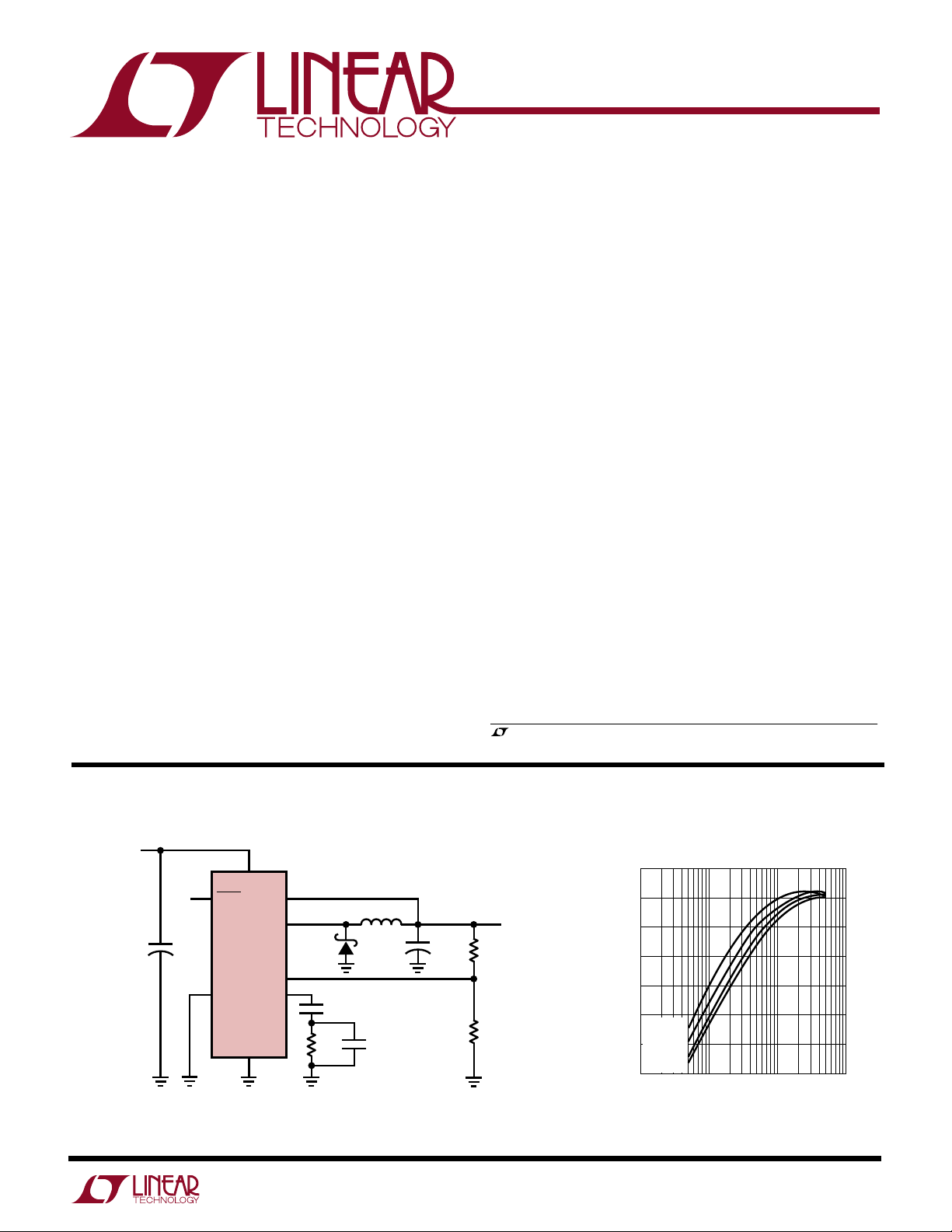
TYPICAL APPLICATIO
V
IN
8V TO 40V
1
+
39µF
63V
6
SHDN
SYNC
V
IN
LT1776
GND
5
4
V
CC
V
SW
FB
V
C
Figure 1
U
2
3
7
8
2200pF
22k
*43T #30 ON MAGNETICS
MPP #55030
100µH*
MBR160
100pF
The available SO-8 package and 200kHz switching frequency allow for minimal PC board area requirements.
, LTC and LT are registered trademarks of Linear Technology Corporation.
Efficiency vs VIN and I
90
80
5V
+
100µF
10V
36.5k
1%
12.1k
1%
1776 F01
400mA
70
60
50
EFFICIENCY (%)
40
VIN = 10V
V
= 20V
IN
30
VIN = 30V
V
= 40V
IN
20
1
10 100 1000
LOAD CURRENT (mA)
LOAD
1776 TA01
1
Page 2
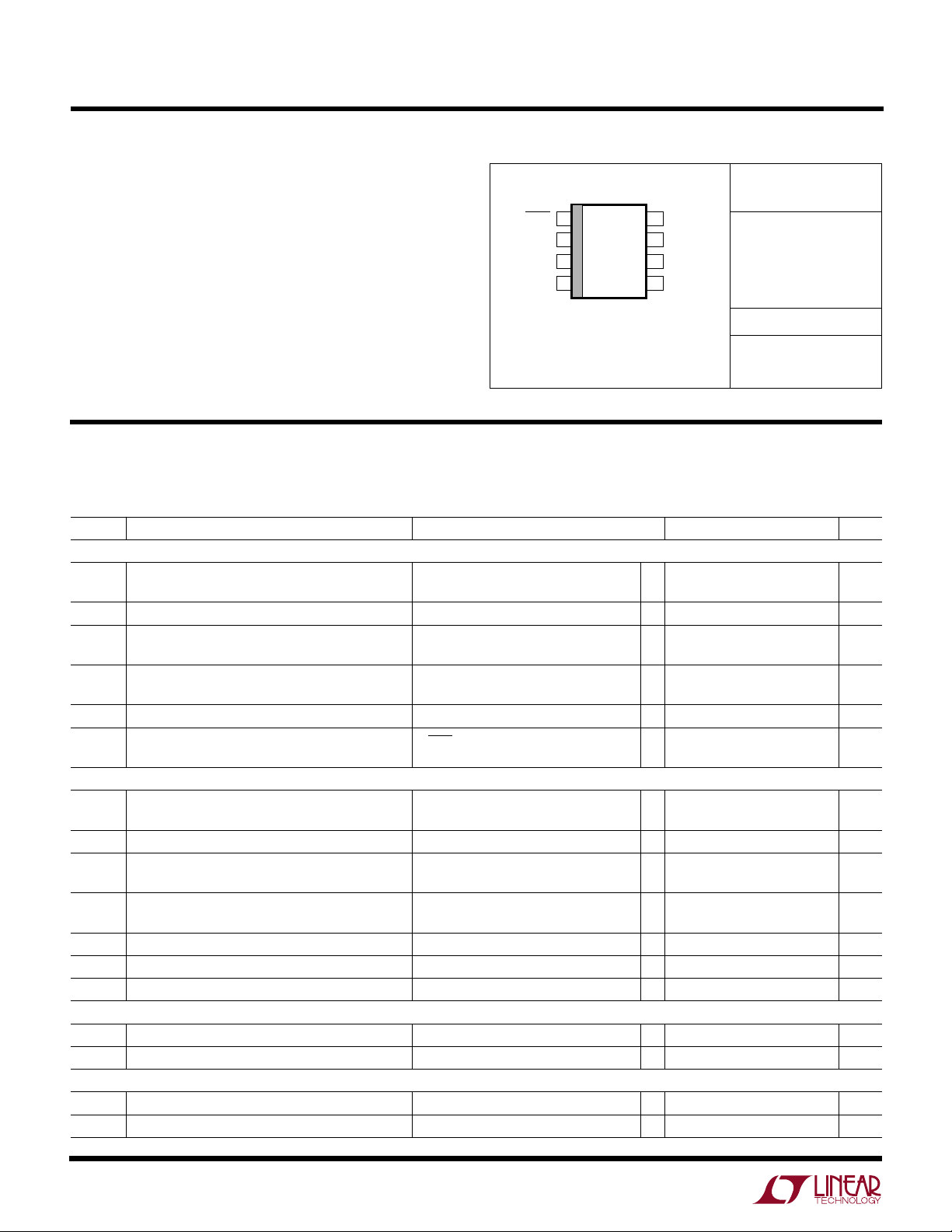
LT1776
1
2
3
4
8
7
6
5
TOP VIEW
V
C
FB
SYNC
V
IN
SHDN
V
CC
V
SW
GND
N8 PACKAGE
8-LEAD PDIP
S8 PACKAGE
8-LEAD PLASTIC SO
WW
W
ABSOLUTE MAXIMUM RA TIN GS
U
U
W
PACKAGE/ORDER INFORMA TION
(Note 1)
Supply Voltage (Note 5) .......................................... 60V
Switch Voltage (Note 5)........................................... 60V
SHDN, SYNC Pin Voltage........................................... 7V
VCC Pin Voltage ....................................................... 30V
FB Pin Voltage ........................................................... 3V
Operating Junction Temperature Range
LT1776C................................................0°C to 125°C
LT1776I............................................ –40°C to 125°C
Storage Temperature Range................. –65°C to 150°C
Lead Temperature (Soldering, 10 sec)..................300°C
T
= 125°C, θJA = 130°C/W (N8)
JMAX
T
= 125°C, θJA = 110°C/W (S8)
JMAX
Consult factory for Military grade parts.
ORDER PART
NUMBER
LT1776CN8
LT1776CS8
LT1776IN8
LT1776IS8
S8 PART MARKING
1776
1776I
ELECTRICAL CHARACTERISTICS
The ● denotes specifications which apply over the full operating temperature range, otherwise specifications are TA = 25°C.
VIN = 40V, VSW open, VCC = 5V, VC = 1.4V unless otherwise noted.
SYMBOL PARAMETER CONDITIONS MIN TYP MAX UNITS
Power Supplies
V
IN(MIN)
I
VIN
I
VCC
V
VCC
Feedback Amplifier
V
REF
I
IN
g
m
I
, I
SRC
V
CL
Output Switch
V
ON
I
LIM
Current Amplifier
2
Minimum Input Voltage 6.7 7.0 V
● 7.4 V
Thermally Limited Continuous Operating Voltage ● 40 V
VIN Supply Current VC = 0V 620 800 µA
● 900 µA
VCC Supply Current VC = 0V 3.2 4.0 mA
● 5.0 mA
VCC Dropout Voltage (Note 2) 2.8 3.1 V
Shutdown Mode I
Reference Voltage 1.225 1.240 1.255 V
FB Pin Input Bias Current 600 1500 nA
Feedback Amplifier Transconductance ∆lc = ±10µA 400 650 1000 µmho
Feedback Amplifier Source or Sink Current 60 100 170 µA
SNK
Feedback Amplifier Clamp Voltage 2.0 V
Reference Voltage Line Regulation 12V ≤ VIN ≤ 60V ● 0.01 %/V
Voltage Gain 200 600 V/V
Output Switch On Voltage ISW = 0.5A 1.0 1.5 V
Switch Current Limit (Note 3) ● 0.55 0.70 1.0 A
Control Pin Threshold Duty Cycle = 0% 0.9 1.1 1.25 V
Control Voltage to Switch Transconductance 2 A/V
VIN
V
= 0V 30 50 µA
SHDN
● 75 µA
● 1.215 1.265 V
● 200 1500 µmho
● 45 220 µA
U
Page 3
LT1776
ELECTRICAL CHARACTERISTICS
The ● denotes specifications which apply over the full operating temperature range, otherwise specifications are TA = 25°C.
VIN = 40V, VSW open, VCC = 5V, VC = 1.4V unless otherwise noted.
SYMBOL PARAMETER CONDITIONS MIN TYP MAX UNITS
Timing
f Switching Frequency 180 200 220 kHz
● 170 230 kHz
Maximum Switch Duty Cycle ● 85 90 %
t
ON(MIN)
Boost Operation
Sync Function
SHDN Pin Function
V
SHDN
I
SHDN
Note 1: Absolute Maximum Ratings are those values beyond which the life
of a device may be impaired.
Note 2: Control circuitry powered from V
Note 3: Switch current limit is DC trimmed and tested in production.
Inductor dl/dt rate will cause a somewhat higher current limit in actual
application.
Note 4: Minimum switch on time is production tested with a 39Ω resistive
load to ground.
Minimum Switch On Time High dV/dt Mode, RL = 39Ω (Note 4) 300 ns
VC Pin Boost Threshold 1.35 V
dV/dt Below Threshold 0.2 V/ns
dV/dt Above Threshold 1.6 V/ns
Minimum Sync Amplitude ● 1.5 2.2 V
Synchronization Range (Note 6) ● 250 400 kHz
SYNC Pin Input R 40 kΩ
Shutdown Mode Threshold 0.5 V
● 0.2 0.8 V
Upper Lockout Threshold Switching Action On 1.260 V
Lower Lockout Threshold Switching Action Off 1.245 V
Shutdown Pin Current V
.
CC
= 0V 12 20 µA
SHDN
= 1.25V 2.5 10 µA
V
SHDN
Note 5: Parts are guaranteed to survive 60V on VIN and VSW. However,
thermal constraints will limit V
on maximum output current and switching frequency. See Applications
section for more information.
Note 6: Internal oscillator is guaranteed to sync up to 400kHz. However,
thermal constraints and/or controllability issues may place a lower limit on
switching frequency in actual usage. See Applications section for more
information.
in some applications, depending primarily
IN
3
Page 4
LT1776
UW
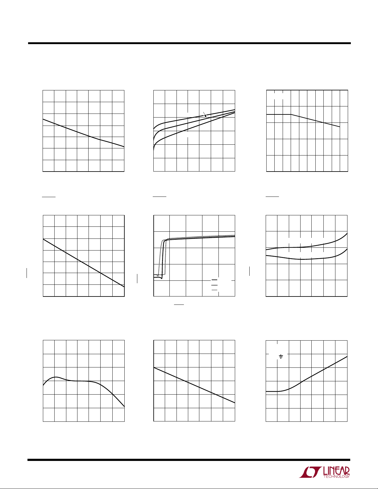
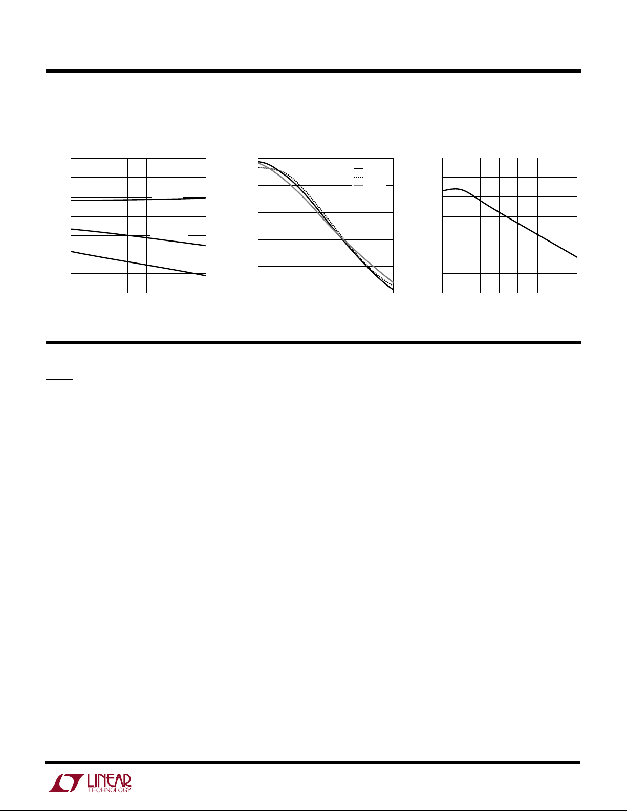
TYPICAL PERFORMANCE CHARACTERISTICS
Minimum Input Voltage vs
Temperature
7.4
7.2
7.0
6.8
6.6
INPUT VOLTAGE (V)
6.4
6.2
6.0
–50
–25 0
TEMPERATURE (°C)
50 100 125
25 75
SHDN Pin Shutdown Threshold
vs Temperature
900
800
700
600
500
400
SHDN PIN VOLTAGE (mV)
300
200
–50
–25 0
TEMPERATURE (°C)
50 100 125
25 75
1776 G01
LT1776 G04
Switch-On Voltage vs
Switch Current
1.50
1.25
1.00
0.75
0.50
SWITCH VOLTAGE (V)
0.25
0
0
–55°C
125°C
100 200
SWITCH CURRENT (mA)
SHDN Pin Input Current
vs Voltage
5
0
–5
–10
–15
SHDN PIN INPUT CURRENT (µA)
–20
1
0
SHDN PIN VOLTAGE (V)
25°C
400 600 700
300 500
3
2
25°C
–55°C
125°C
4
1776 G02
1776 G05
Switch Current Limit vs
Duty Cycle
1000
TA = 25°C
800
600
400
200
SWITCH CURRENT LIMIT (mA)
0
2010 30 50 70 90
0
DUTY CYCLE (%)
60
80
40
100
1776 G03
SHDN Pin Lockout Thresholds
vs Temperature
1.30
1.28
UPPER THRESHOLD
1.26
LOWER THRESHOLD
1.24
SHDN PIN VOLTAGE (V)
1.22
5
1.20
–50
–25 0
TEMPERATURE (°C)
50 100 125
25 75
LT1776 G06
Switching Frequency
vs Temperature
215
210
205
200
195
SWITCHING FREQUENCY (kHz)
190
185
–50 25 75
–25 0
TEMPERATURE (°C)
4
50 100 125
1776 G07
Minimum Synchronization Voltage
vs Temperature
2.25
2.00
1.75
1.50
1.25
1.00
MINIMUM SYNCHRONIZATION VOLTAGE (V)
0.75
–50 25 75
–25 0
TEMPERATURE (°C)
50 100 125
1776 G08
Switch Minimum On-Time
vs Temperature
600
V
= 40V
IN
= 39Ω
R
L
500
FB =
400
300
200
100
SWITCH MINIMUM ON-TIME (ns)
0
–50 25 75
–25 0
TEMPERATURE (°C)
50 100 125
1776 G09
Page 5
UW
TYPICAL PERFORMANCE CHARACTERISTICS
VC Pin Switching Threshold,
Boost Threshold, Clamp Voltage
vs Temperature
2.2
2.0
1.8
1.6
1.4
PIN VOLTAGE (V)
C
V
1.2
1.0
0.8
–50
–25 0
25 75
TEMPERATURE (°C)
CLAMP
VOLTAGE
THRESHOLD
SWITCHING
THRESHOLD
50 100 125
BOOST
LT1776 G10
Feedback Amplifier Output
Current vs FB Pin Voltage
100
50
0
–50
–100
FEEDBACK AMPLIFIER OUTPUT CURRENT (µA)
–150
1.0
1.1
1.2
FB PIN VOLTAGE (V)
1.3
1.4
UUU
PIN FUNCTIONS
25°C
–55°C
125°C
1776 G11
1.5
LT1776
Error Amplifier Transconductance
vs Temperature
750
700
650
600
550
500
TRANSCONDUCTANCE (µmho)
450
400
–50
–25 0
TEMPERATURE (°C)
50 100 125
25 75
LT1776 G12
SHDN (Pin 1): When pulled below the shutdown mode
threshold, nominally 0.30V, this pin turns off the regulator
and reduces VIN input current to a few tens of microamperes (shutdown mode).
When this pin is held above the shutdown mode threshold,
but below the lockout threshold, the part will be operational with the exception that output switching action will
be inhibited (lockout mode). A user-adjustable undervoltage lockout can be implemented by driving this pin from
an external resistor divider to VIN. This action is logically
“ANDed” with the internal UVLO, set at nominally 6.7V,
such that minimum VIN can be increased above 6.7V, but
not decreased (see Applications Information).
If unused, this pin should be left open. However, the high
impedance nature of this pin renders it susceptible to
coupling from the high speed VSW node, so a small
capacitor to ground, typically 100pF or so is recommended when the pin is left “open”.
VCC (Pin 2): This pin is used to power the internal control
circuitry off of the switching supply output. Proper use of
this pin enhances overall power supply efficiency. During
start-up conditions, internal control circuitry is powered
directly from VIN.
If the output capacitor is located more than one inch from
the VCC pin, a separate 0.1µF bypass capacitor to ground
may be required right at the pin.
VSW (Pin 3): This is the emitter node of the output switch
and has large currents flowing through it. This node
moves at a high dV/dt rate, especially when in “boost”
mode. Keep the traces to the switching components as
short as possible to minimize electromagnetic radiation
and voltage spikes.
GND (Pin 4): This is the device ground pin. The internal
reference and feedback amplifier are referred to it. Keep
the ground path connection to the FB divider and the V
C
compensation capacitor free of large ground currents.
VIN (Pin 5): This is the high voltage supply pin for the
output switch. It also supplies power to the internal control
circuitry during start-up conditions or if the VCC pin is left
open. A high quality bypass capacitor which meets the
input ripple current requirements is needed here. (See
Applications Information).
SYNC (Pin 6): Pin used to synchronize internal oscillator
to the external frequency reference. It is directly logic
compatible and can be driven with any signal between
5
Page 6
LT1776
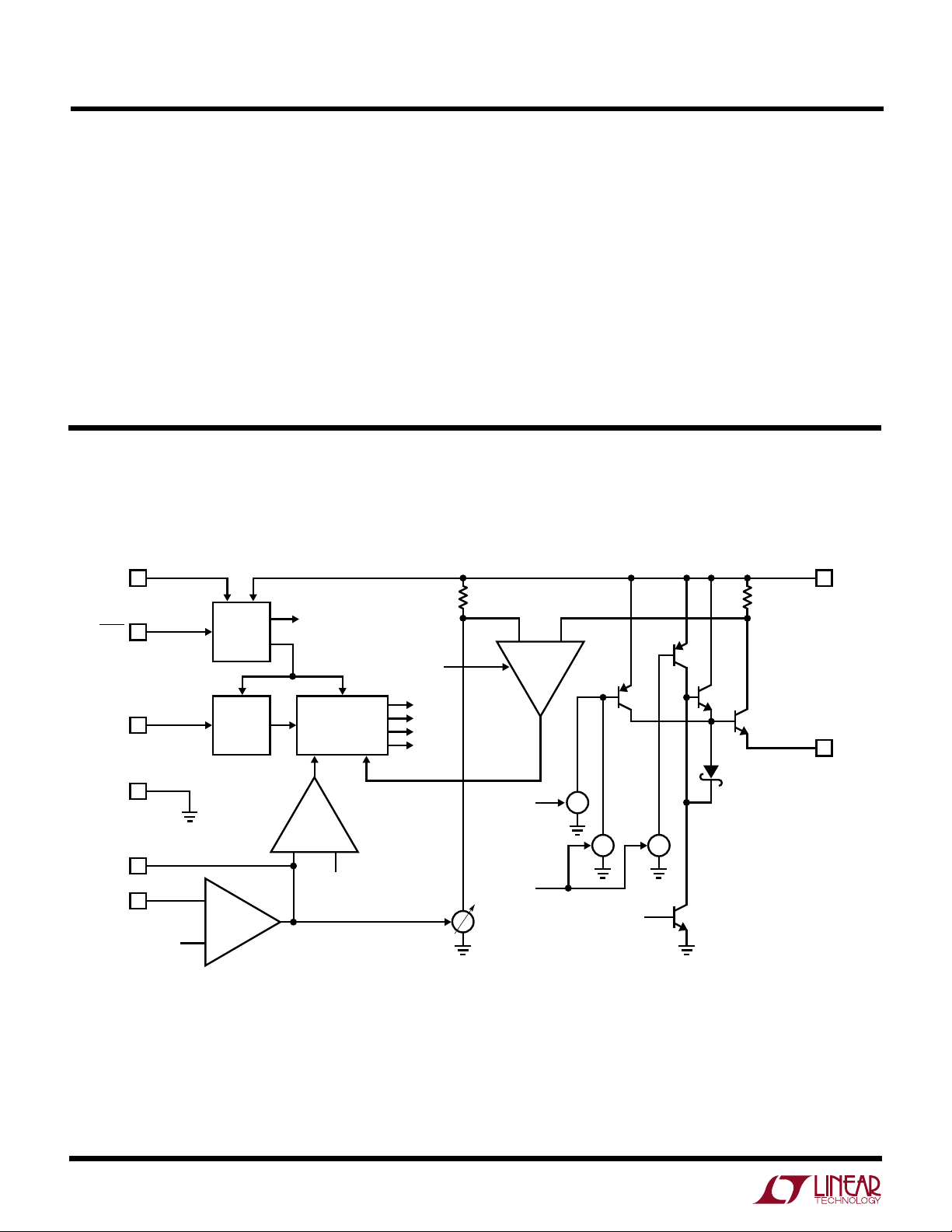
SWDR
SWDR
SWON
SWON
BOOST
1776 BD
BOOST
SWOFF
SWOFF
LOGICOSC
BIAS
V
TH
V
B
V
BG
V
BG
FB
V
C
GND
SYNC
SHDN
V
CC
FB
AMP
BOOST
COMP
gm
I
I
I I
R1 R
SENSE
I
COMP
Q4
Q3
Q2
Q1
Q5
V
SW
D1
V
IN
5
3
2
1
6
4
8
7
UUU
PIN FUNCTIONS
10% and 90% duty cycle. The sync function is internally
disabled if the FB pin voltage is low enough to cause
oscillator slowdown. If unused, this pin should be grounded.
FB (Pin 7): This is the inverting input to the feedback
amplifier. The noninverting input of this amplifier is internally tied to the 1.24V reference. This pin also slows down
the frequency of the internal oscillator when its voltage is
W
BLOCK DIAGRA
abnormally low, e.g., 2/3 of normal or less. This feature
helps maintain proper short-circuit protection.
VC (Pin 8): This is the control voltage pin which is the
output of the feedback amplifier and the input of the
current comparator. Frequency compensation of the overall loop is effected by placing a capacitor, (or in most cases
a series RC combination) between this node and ground.
6
Page 7

WUW
TIMING DIAGRAMS
LT1776
Low dV/dt ModeHigh dV/dt Mode
V
IN
V
SW
0
SWDR
SWON
BOOST
SWOFF
1776 TD01
U
OPERATIO
The LT1776 is a current mode switching regulator IC that
has been optimized for high efficiency operation in high
input voltage, low output voltage buck topologies. The
Block Diagram shows an overall view of the system.
Several of the blocks are straightforward and similar to
those found in traditional designs, including: Internal Bias
Regulator, Oscillator and Feedback Amplifier. The novel
portion includes an elaborate Output Switch section and
Logic Section to provide the control signals required by
the switch section.
The LT1776 operates much the same as traditional
current mode switchers, the major difference being its
specialized output switch section. Due to space constraints, this discussion will not reiterate the basics of
current mode switcher/controllers and the “buck” topology. A good source of information on these topics is
Application Note 19.
Output Switch Theory
One of the classic problems in delivering low output
voltage from high input voltage at good efficiency is that
minimizing AC switching losses requires very fast voltage (dV/dt) and current (dI/dt) transition at the output
device. This is in spite of the fact that in a bipolar
implementation, slow lateral PNPs must be included in
the switching signal path.
V
IN
V
SW
0
SWDR
SWON
BOOST
SWOFF
1776 TD02
Fast positive-going slew rate action is provided by lateral
PNP Q3 driving the Darlington arrangement of Q1 and Q2.
The extra β available from Q2 greatly reduces the drive
requirements of Q3.
Although desirable for dynamic reasons, this topology
alone will yield a large DC forward voltage drop. A second
lateral PNP, Q4, acts directly on the base of Q1 to reduce
the voltage drop after the slewing phase has taken place.
To achieve the desired high slew rate, PNPs Q3 and Q4 are
“force-fed” packets of charge via the current sources
controlled by the boost signal.
Please refer to the High dV/dt Mode Timing Diagram. A
typical oscillator cycle is as follows: The logic section first
generates an SWDR signal that powers up the current
comparator and allows it time to settle. About 1µs later, the
SWON signal is asserted and the BOOST signal is pulsed
for a few hundred nanoseconds. After a short delay, the
VSW pin slews rapidly to VIN. Later, after the peak switch
current indicated by the control voltage VC has been
reached (current mode control), the SWON and SWDR
signals are turned off, and SWOFF is pulsed for several
hundred nanoseconds. The use of an explicit turn-off
device, i.e., Q5, improves turn-off response time and thus
aids both controllability and efficiency.
7
Page 8

LT1776
OPERATIO
U
The system as previously described handles heavy loads
(continuous mode) at good efficiency, but it is actually
counterproductive for light loads. The method of jamming charge into the PNP bases makes it difficult to turn
them off rapidly and achieve the very short switch ON
times required by light loads in discontinuous mode.
Further
adversely affects light load controllability.
The solution is to employ a “boost comparator” whose
inputs are the VC control voltage and a fixed internal
threshold reference, VTH. (Remember that in a current
mode switching topology, the VC voltage determines the
peak switch current.) When the VC signal is above VTH, the
previously described “high dV/dt” action is performed.
When the VC signal is below VTH, the boost pulses are
absent, as can be seen in the Low dV/dt Mode Timing
Diagram. Now the DC current, activated by the SWON
more, the high leading edge dV/dt rate similarly
U
WUU
APPLICATIONS INFORMATION
signal alone, drives Q4 and this transistor drives Q1 by
itself. The absence of a boost pulse, plus the lack of a
second NPN driver, result in a much lower slew rate which
aids light load controllability.
A further aid to overall efficiency is provided by the
specialized bias regulator circuit, which has a pair of
inputs, VIN and VCC. The VCC pin is normally connected to
the switching supply output. During start-up conditions,
the LT1776 powers itself directly from VIN. However, after
the switching supply output voltage reaches about 2.9V,
the bias regulator uses this supply as its input. Previous
generation buck controller ICs without this provision
typically required hundreds of milliwatts of quiescent
power when operating at high input voltage. This both
degraded efficiency and limited available output current
due to internal heating.
Selecting a Power Inductor
There are several parameters to consider when selecting
a power inductor. These include inductance value, peak
current rating (to avoid core saturation), DC resistance,
construction type, physical size, and of course, cost.
In a typical application, proper inductance value is dictated
by matching the discontinuous/continuous crossover point
with the LT1776 internal low-to-high dV/dt threshold. This
is the best compromise between maintaining control with
light loads while maintaining good efficiency with heavy
loads. The fixed internal dV/dt threshold has a nominal
value of 1.4V, which referred to the VC pin threshold and
control voltage to switch transconductance, corresponds
to a peak current of about 200mA. Standard buck converter theory yields the following expression for inductance at the discontinuous/continuous crossover:
L
=
V
OUT
•
fI
PK
–
VV
IN OUT
V
IN
For example, substituting 40V, 5V, 200mA and 200kHz
respectively for VIN, V
100µH. Note that the left half of this expression is indepen-
dent of input voltage while the right half is only a weak
function of VIN when VIN is much greater than V
means that a single inductor value will work well over a
range of “high” input voltage. And although a progressively smaller inductor is suggested as VIN begins to
approach V
under these conditions are much more forgiving with
respect to controllability and efficiency issues. Therefore
when a wide input voltage range must be accommodated,
say 10V to 40V for 5V
inductance value based on the maximum input voltage.
Once the inductance value is decided, inductor peak
current rating and resistance need to be considered. Here,
the inductor peak current rating refers to the onset of
saturation in the core material, although manufacturers
sometimes specify a “peak current rating” which is derived from a worst-case combination of core saturation
and self-heating effects. Inductor winding resistance alone
, note that the much higher ON duty cycles
OUT
, IPK and f yields a value of about
OUT
OUT
, the user should choose an
OUT
. This
8
Page 9

LT1776
U
WUU
APPLICATIONS INFORMATION
limits the inductor’s current carrying capability as the I2R
power threatens to overheat the inductor. If applicable,
remember to include the condition of output short circuit.
Although the peak current rating of the inductor can be
exceeded in short-circuit operation, as core saturation per
se is not destructive to the core, excess resistive selfheating is still a potential problem.
The final inductor selection is generally based on cost,
which usually translates into choosing the smallest physical size part that meets the desired inductance value,
resistance and current carrying capability. An additional
factor to consider is that of physical construction. Briefly
stated, “open” inductors built on a rod- or barrel-shaped
core generally offer the smallest physical size and lowest
cost. However their open construction does not contain
the resulting magnetic field, and they may not be acceptable in RFI-sensitive applications. Toroidal style inductors, many available in surface mount configuration, offer
improved RFI performance, generally at an increase in
cost and physical size. And although custom design is
always a possibility, most potential LT1776 applications
can be handled by the array of standard, off-the-shelf
inductor products offered by the major suppliers.
Selecting Freewheeling Diode
Highest efficiency operation requires the use of a Schottky
type diode. DC switching losses are minimized due to its
low forward voltage drop, and AC behavior is benign due
to its lack of a significant reverse recovery time. Schottky
diodes are generally available with reverse voltage ratings
of 60V and even 100V, and are price competitive with other
types.
The use of so-called “ultrafast” recovery diodes is generally not recommended. When operating in continuous
mode, the reverse recovery time exhibited by “ultrafast”
diodes will result in a slingshot type effect. The power
internal switch will ramp up VIN current into the diode in an
attempt to get it to recover. Then, when the diode has
finally turned off, some tens of nanoseconds later, the V
node voltage ramps up at an extremely high dV/dt, perhaps 5 to even 10V/ns! With real world lead inductances,
the VSW node can easily overshoot the VIN rail. This can
SW
result in poor RFI behavior and if the overshoot is severe
enough, damage the IC itself.
Selecting Bypass Capacitors
The basic topology as shown in Figure 1 uses two bypass
capacitors, one for the VIN input supply and one for the
V
output supply.
OUT
User selection of an appropriate output capacitor is relatively easy, as this capacitor sees only the AC ripple current
in the inductor. As the LT1776 is designed for buck or
step-down applications, output voltage will nearly always
be compatible with tantalum type capacitors, which are
generally available in ratings up to 35V or so. These
tantalum types offer good volumetric efficiency and many
are available with specified ESR performance. The product
of inductor AC ripple current and output capacitor ESR will
manifest itself as peak-to-peak voltage ripple on the output
node. (Note: If this ripple becomes too large, heavier
control loop compensation, at least at the switching frequency, may be required on the VC pin.) The most demanding applications, requiring very low output ripple,
may be best served not with a single extremely large
output capacitor, but instead by the common technique of
a separate L/C lowpass post filter in series with the output.
(In this case, “Two caps are better than one”.)
The input bypass capacitor is normally a more difficult
choice. In a typical application e.g., 40VIN to 5V
relatively heavy VIN current is drawn by the power switch
for only a small portion of the oscillator period (low ON
duty cycle). The resulting RMS ripple current, for which
the capacitor must be rated, is often several times the DC
average VIN current. Similarly, the “glitch” seen on the V
supply as the power switch turns on and off will be related
to the product of capacitor ESR, and the relatively high
instantaneous current drawn by the switch. To compound
these problems is the fact that most of these applications
will be designed for a relatively high input voltage, for
which tantalum capacitors are generally unavailable. Relatively bulky “high frequency” aluminum electrolytic types,
specifically constructed and rated for switching supply
applications, may be the only choice.
OUT
,
IN
9
Page 10

LT1776
U
WUU
APPLICATIONS INFORMATION
Input Voltage vs Operating Frequency Considerations
The absolute maximum input supply voltage for the LT1776
is specified at 60V. This is based solely on internal semiconductor junction breakdown effects. Due to internal
power dissipation, the actual maximum VIN achievable in
a particular application may be less than this.
A detailed theoretical basis for estimating internal power
loss is given in the section, Thermal Considerations. Note
that AC switching loss is proportional to both operating
frequency and output current. The majority of AC switching loss is also proportional to the square of input voltage.
For example, while the combination of VIN = 40V, V
5V at 500mA and f
simultaneously raising VIN to 60V and f
not possible. Nevertheless, input voltage
60V can usually be accommodated, assuming the resulting increase in internal dissipation is of insufficient time
duration to raise die temperature significantly.
A second consideration is controllability. A potential limitation occurs with a high step-down ratio of VIN to V
as this requires a correspondingly narrow minimum switch
ON time. An approximate expression for this (assuming
continuous mode operation) is given as follows:
= 200kHz may be easily achievable,
OSC
to 400kHz is
OSC
transients
=
OUT
up to
OUT
,
resulting ramping current behavior helps overdrive the
current comparator (current mode switching) and reduce
its propagation delay, hastening output switch turnoff.
Second, and more importantly, actual power supply operation involves a feedback amplifier that adjusts the V
node control voltage to maintain proper output voltage. As
progressively shorter ON times are required, the feedback
loop acts to reduce VC, and the resulting overdrive further
reduces the propagation delay in the current comparator.
A suggested worst-case limit for minimum switch ON time
in actual operation is 350ns.
A potential controllability problem arises if the LT1776 is
called upon to produce an ON time shorter than its ability.
Feedback loop action will lower then reduce the VC control
voltage to the point where some sort of cycle-skipping or
odd/even cycle behavior is exhibited.
In summary:
1. Be aware that the simultaneous requirements of high
VIN, high I
practice due to internal dissipation. The Thermal Considerations section offers a basis to estimate internal
power. In questionable cases a prototype supply should
be built and exercised to verify acceptable operation.
and high f
OUT
may not be achievable in
OSC
C
VV
+
ON
OUT F
Vf
()
IN OSC
SW
M
in t =
where:
VIN = input voltage
V
= output voltage
OUT
VF = Schottky diode forward drop
f
= switching frequency
OSC
It is important to understand the nature of minimum
switch ON time as given in the data sheet. This test is
intended to mimic behavior under short-circuit conditions. It is performed with the VC control voltage at its
clamp level (VCL) and uses a fixed resistive load from V
to ground for simplicity. The resulting ON time behavior is
overconservative as a general operating design value for
two reasons. First, actual power supply application circuits present an inductive load to the VSW node. The
2. The simultaneous requirements of high VIN, low V
and high f
minimum switch ON time. Cycle skipping and/or odd/
even cycle behavior will result although correct output
voltage is usually maintained.
Minimum Load Considerations
As discussed previously, a lightly loaded LT1776 with V
pin control voltage below the boost threshold will operate
in low dV/dt mode. This affords greater controllability at
light loads, as minimum tON requirements are relaxed.
However, some users may be indifferent to pulse skipping
behavior, but instead may be concerned with maintaining
maximum possible efficiency at light loads. This requirement can be satisfied by forcing the part into Burst Mode
operation. The use of an external comparator whose
Burst Mode is a trademark of Linear Technology Corporation.
can result in an unacceptably short
OSC
OUT
C
TM
10
Page 11

LT1776
FB DIVIDER THEVENIN VOLTAGE (V)
0
f
OSC
(kHz)
0
50
100
150
200
0.25 0.50 0.75 1.00
1776 F02
1.25
R
TH
LT1776
FB
RTH = 22k
R
TH
= 10k
R
TH
= 4.7k
U
WUU
APPLICATIONS INFORMATION
output controls the shutdown pin allows high efficiency at
light loads through Burst Mode operation behavior (see
Typical Applications and Figure 8).
Maximum Load/Short-Circuit Considerations
The LT1776 is a current mode controller. It uses the V
node voltage as an input to a current comparator which
turns off the output switch on a cycle-by-cycle basis as
this peak current is reached. The internal clamp on the V
node, nominally 2V, then acts as an output switch peak
current limit. This action becomes the switch current limit
specification. The maximum available output power is
then determined by the switch current limit.
A potential controllability problem could occur under
short-circuit conditions. If the power supply output is
short circuited, the feedback amplifier responds to the low
output voltage by raising the control voltage, VC, to its
peak current limit value. Ideally, the output switch would
be turned on, and then turned off as its current exceeded
the value indicated by VC. However, there is finite response
time involved in both the current comparator and turnoff
of the output switch. These result in a minimum ON time
t
ON(MIN)
. When combined with the large ratio of VIN to
(VF + I • R), the diode forward voltage plus inductor I • R
voltage drop, the potential exists for a loss of control.
Expressed mathematically the requirement to maintain
control is:
C
C
The solution to this dilemma is to slow down the oscillator
when the FB pin voltage is abnormally low thereby indicating some sort of short-circuit condition. Figure 2 shows
the typical response of Oscillator Frequency vs FB divider
Thevenin voltage and impedance. Oscillator frequency is
unaffected until FB voltage drops to about 2/3 of its normal
value. Below this point the oscillator frequency decreases
roughly linearly down to a limit of about 30kHz. This lower
oscillator frequency during short-circuit conditions can
then maintain control with the effective minimum ON time.
A further potential problem with short-circuit operation
might occur if the user were operating the part with its
oscillator slaved to an external frequency source via the
SYNC pin. However, the LT1776 has circuitry that automatically disables the sync function when the oscillator is
slowed down due to abnormally low FB voltage.
VIR
•≤+
ft
•
ON
F
V
IN
where:
f = switching frequency
tON = switch ON time
VF = diode forward voltage
VIN = Input voltage
I • R = inductor I • R voltage drop
If this condition is not observed, the current will not be
limited at IPK, but will cycle-by-cycle ratchet up to some
higher value. Using the nominal LT1776 clock frequency
of 200KHz, a VIN of 40V and a (VF + I • R) of say 0.7V, the
maximum tON to maintain control would be approximately
90ns, an unacceptably short time.
Figure 2. Oscillator Frequency vs FB Divider
Thevenin Voltage and Impedance
Feedback Divider Considerations
An LT1776 application typically includes a resistive divider
between V
the FB pin to the reference voltage V
and ground, the center node of which drives
OUT
. This establishes
REF
a fixed ratio between the two resistors, but a second
degree of freedom is offered by the overall impedance level
of the resistor pair. The most obvious effect this has is one
of efficiency — a higher resistance feedback divider will
waste less power and offer somewhat higher efficiency,
especially at light load.
11
Page 12

LT1776
U
WUU
APPLICATIONS INFORMATION
However, remember that oscillator slowdown to achieve
short-circuit protection (discussed above) is dependent
on FB pin behavior, and this in turn, is sensitive to FB node
external impedance. Figure 2 shows the typical relationship between FB divider Thevenin voltage and impedance,
and oscillator frequency. This shows that as feedback
network impedance increases beyond 10k, complete oscillator slowdown is not achieved, and short-circuit protection may be compromised. And as a practical matter,
the product of FB pin bias current and larger FB network
impedances will cause increasing output voltage error.
(Nominal cancellation for 10k of FB Thevenin impedance
is included internally.)
Thermal Considerations
Care should be taken to ensure that the worst-case input
voltage and load current conditions do not cause excessive die temperatures. The packages are rated at 110°C/W
for the 8-pin SO (S8) and 130°C/W for 8-pin PDIP (N8).
Quiescent power is given by:
PQ = IIN • VIN + I
(This assumes that the VCC pin is connected to V
Power loss internal to the LT1776 related to actual output
current is composed of both DC and AC switching losses.
These can be roughly estimated as follows:
VCC
• V
OUT
OUT
.)
PAC = 1/2 • V
tr = (VIN/1.6)ns in high dV/dt mode
(VIN/0.16)ns in low dV/dt mode
tf = (VIN/1.6)ns (irrespective of dV/dt mode)
f = switching frequency
Total power dissipation of the die is simply the sum of
quiescent, DC and AC losses previously calculated.
P
D(TOTAL)
Frequency Compensation
Loop frequency compensation is performed by connecting a capacitor, or in most cases a series RC, from the
output of the error amplifier (VC pin) to ground. Proper
loop compensation may be obtained by empirical methods as described in detail in Application Note 19. Briefly,
this involves applying a load transient and observing the
dynamic response over the expected range of VIN and
I
values.
LOAD
As a practical matter, a second small capacitor, directly
from the VC pin to ground is generally recommended to
attenuate capacitive coupling from the V
value for this capacitor is 100pF. (See Switch Node Considerations).
Switch Node Considerations
• I
IN
= PQ + PDC + P
• (tr + tf + 30ns) • f
OUT
AC
pin. A typical
SW
DC switching losses are dominated by output switch “ON
voltage”, i.e.,
PDC = V
VON = Output switch ON voltage, typically 1V at 500mA
I
= Output current
OUT
DC = ON duty cycle
AC switching losses are typically dominated by power lost
due to the finite rise time and fall time at the VSW node.
Assuming, for simplicity, a linear ramp up of both voltage
and current and a current rise/fall time equal to 15ns,
ON
• I
OUT
• DC
12
For maximum efficiency, switch rise and fall times are
made as short as practical. To prevent radiation and high
frequency resonance problems, proper layout of the components connected to the IC is essential, especially the
power path. B field (magnetic) radiation is minimized by
keeping output diode, switch pin and input bypass capacitor leads as short as possible. E field radiation is kept low
by minimizing the length and area of all traces connected
to the switch pin (VSW). A ground plane should always be
used under the switcher circuitry to prevent interplane
coupling.
Page 13

LT1776
U
WUU
APPLICATIONS INFORMATION
The high speed switching current path is shown schematically in Figure 3. Minimum lead length in these paths is
essential to ensure clean switching and minimal EMI. The
paths containing the input capacitor, output switch and
output diode are the only ones containing nanosecond rise
and fall times. Keep these paths as short as possible.
V
IN
+
V
IN
Figure 3. High Speed Current Switching Paths
Additionally, it is possible for the LT1776 to cause EMI
problems by “coupling to itself”. Specifically, this can
occur if the VSW pin is allowed to capacitively couple in an
uncontrolled manner to the part’s high impedance nodes,
i.e., SHDN, SYNC, VC and FB. This can cause erratic
operation such as odd/even cycle behavior, pulse width
“nervousness”, improper output voltage and/or premature current limit action.
LT1776
C1
V
SW
+
D1
V
OUT
C2
1776 F03
As an example, assume that the capacitance between the
VSW node and a high impedance pin node is 0.1pF, and
further assume that the high impedance node in question
exhibits a capacitance of 1pF to ground. Due to the high
dV/dt, large excursion behavior of the VSW node, this will
couple a nearly 4V transient to the high impedance pin,
causing abnormal operation. (This assumes the “typical”
40VIN to 5V
application.) An explicit 100pF capacitor
OUT
added to the node will reduce the amplitude of the disturbance to more like 50mV (although settling time will
increase).
Specific pin recommendations are as follows:
SHDN: If unused, add a 100pF capacitor to ground.
SYNC: Ground if unused.
VC: Add a capacitor directly to ground in addition to the
explicit compensation network. A value of one-tenth of
the main compensation capacitor is recommended, up
to a maximum of 100pF.
FB: Assuming the VC pin is handled properly, this pin
usually requires no explicit capacitor of its own, but
keep this node physically small to minimize stray
capacitance.
13
Page 14

LT1776
U
TYPICAL APPLICATIONS
Minimum Component Count Application
Figure 4a shows a basic “minimum component count”
application. The circuit produces 5V at up to 500mA I
OUT
with input voltages in the range of 10V to 40V. The typical
P
OUT/PIN
efficiency is shown in Figure 4b. As shown, the
SHDN and SYNC pins are unused, however either (or both)
can be optionally driven by external signals as desired.
V
IN
10V TO
40V
1
+
C1
39µF
63V
C1: PANASONIC HFQ
C2: AVX D CASE TPSD107M010R0080
C4, C5: X7R OR COG/NPO
D1: MOTOROLA 100V, 1A, SMD SCHOTTKY
L1: COILCRAFT DO3316P-104
C5
100pF
6
SHDN
SYNC
V
IN
LT1776
GND
5
V
CC
V
SW
FB
V
C
4
User-Programmable Undervoltage Lockout
Figure 5 adds a resistor divider to the basic application.
This is a simple, cost-effective way to add a userprogrammable undervoltage lockout (UVLO) function.
Resistor R5 is chosen to have approximately 200µA
through it at the nominal SHDN pin lockout threshold of
1.25V. The somewhat arbitrary value of 200µA was
2
V
R1
36.5k
1%
R2
12.1k
1%
1776 F04a
OUT
5V
0mA to 500mA
3
D1
MBRS1100
7
8
C3
2200pF
X7R
R3
22k
5%
FOR 3.3V V
R1: 24.3K, R2: 14.7k
L1: 68µH, DO3316P-683
I
OUT
VERSION:
OUT
: 0mA TO 500mA
L1
100µH
C4
100pF
+
C2
100µF
10V
Figure 4a. Minimum Component Count Application
90
80
70
60
50
EFFICIENCY (%)
40
VIN = 10V
30
= 20V
V
IN
= 30V
V
IN
20
1
Figure 4b. P
V
= 40V
IN
10 100 1000
I
(mA)
LOAD
OUT/PIN
Efficiency
1776 F04b
14
Page 15

U
TYPICAL APPLICATIONS
V
IN
R4
158k
1%
R5
6.19k
1%
Figure 5. User Programmable Undervoltage Lockout
LT1776
+
C1
1
C5
6
SHDN
SYNC
V
IN
LT1776
GND
5
2
V
CC
3
V
SW
7
FB
8
V
C
C3
4
R3
L1
D1
+
C2
C4
R1
R2
1776 F05
V
OUT
chosen to be significantly above the SHDN pin input
current to minimize its error contribution, but significantly below the typical 3.8mA the LT1776 draws in
lockout mode. Resistor R4 is then chosen to yield this
same 200µA, less 2.5µA, with the desired VIN UVLO
voltage minus 1.25V applied across it. (The 2.5µA factor
is an allowance to minimize error due to SHDN pin input
current.)
Behavior is as follows: Normal operation is observed at the
nominal input voltage of 40V. As the input voltage is
decreased to roughly 32V, switching action will stop, V
will drop to zero, and the LT1776 will draw its VIN and V
OUT
CC
quiescent currents from the VIN supply. At a much lower
input voltage, typically 14V or so at 25°C, the voltage on
the SHDN pin will drop to the shutdown threshold, and the
part will draw its shutdown current only from the VIN rail.
The resistive divider of R4 and R5 will continue to draw
power from VIN. (The user should be aware that while the
SHDN pin
ing temperature effects, the SHDN pin
lockout
threshold is relatively accurate includ-
shutdown
threshold is more coarse, and exhibits considerably more
temperature drift. Nevertheless the shutdown threshold
will always be well below the lockout threshold.)
Minimum Size Inductor Application
Figure 4a employs power path parts that are capable of
delivering the full rated output capability of the LT1776.
Potential users with low output current requirements may
be interested in substituting a physically smaller and less
costly power inductor. The circuit shown in Figure 6a is
topologically identical to the basic application, but specifies a much smaller inductor. This circuit is capable of
delivering up to 400mA at 5V, or, up to 500mA at 3.3V. The
only disadvantage is that due to the increased resistance
in the inductor, the circuit is no longer capable of withstanding indefinite short circuits to ground. The LT1776
will still current limit at its nominal I
value, but this will
LIM
overheat the inductor. Momentary short circuits of a few
seconds or less can still be tolerated. Typical efficiency is
shown in Figure 6b.
15
Page 16

LT1776
U
TYPICAL APPLICATIONS
V
IN
10V TO
40V
+
C1
C1: PANASONIC HFQ 39µF AT 63V
C2: AVX D CASE 100µF 10V
TPSD107M010R0080
C3: 2200pF, X7R
5
V
IN
1
SHDN
C5
LT1776
6
SYNC
GND
C4, C5: 100pF, X7R OR COG/NPO
D1: MOTOROLA 100V, 1A, SMD SCHOTTKY
MBRS1100 (T3)
L1: COILCRAFT DO1608C-683
2
V
CC
3
V
SW
7
FB
8
V
C
4
R3
22k
5%
L1
68µH
+
C2
C4
D1
C3
V
OUT
5V
0mA to 400mA
R1
36.5k
1%
R2
12.1k
1%
1776 F06a
FOR 3.3V V
I
OUT
L1: 47µH, DO1608C-473
R1: 24.3K, R2: 14.7k
VERSION:
OUT
: 0mA TO 500mA
(a)
90
80
70
60
50
EFFICIENCY (%)
VIN = 10V
40
= 20V
V
IN
30
V
= 30V
IN
20
1
= 40V
V
IN
10 100 1000
LOAD CURRENT (mA)
Figure 6. Minimum Inductor Size Application
Burst Mode Operation Configuration
Figure 4b demonstrates that power supply efficiency degrades with lower output load current. This is not surprising, as the LT1776 itself represents a fixed power overhead.
A possible way to improve light load efficiency is in Burst
Mode operation.
Figure 7 shows the LT1776 configured for Burst Mode
operation. Output voltage regulation is now provided in a
1776 F06b
(b)
“bang-bang” digital manner, via comparator U2, an
LTC1440. Resistor divider R3/R4 provides a scaled version of the output voltage, which is compared against U2’s
internal reference. Intentional hysteresis is set by the R5/
R6 divider. As the output voltage falls below the regulation
range, the LT1776 is turned on. The output voltage rises,
and as it climbs above the regulation range, the LT1776 is
turned off. Efficiency is maximized, as the LT1776 is only
powered up while it is providing heavy output current.
16
Page 17

U
TYPICAL APPLICATIONS
LT1776
V
IN
+
C1
R7
10M
Q1
PN2484
Q2
2N2369
NC
C1: PANASONIC HFQ 39µF AT 63V
C2: AVX D CASE 100µF 10V
TPSD107M010R0080
D1: MOTOROLA 100V, 1A,
SMD SCHOTTKY
MBRS1100 (T3)
L1: COILCRAFT DO3316-104
5
V
IN
4
7
+
HYST
GND
V
V
REF
2
CC
3
SW
7
FB
8
V
C
3
+
IN
4
–
IN
6
5
12
D1
C3
100pF
L1
R5
22k
R6
2.4M
V
OUT
+
R1
C2
39k
5%
R2
10k
5%
5V
R3
323k
1%
R4
100k
1%
1776 F07a
6
SYNC
U1
LT1776
1
SHDN
GND
V
8
OUT
U2
LTC1440
–
V
(a)
90
80
VIN = 10V
70
60
50
EFFICIENCY (%)
40
30
20
VIN = 40V
VIN = 30V
V
= 20V
IN
1
10 100 1000
LOAD CURRENT (mA)
1776 F07b
(b)
Figure 7. Burst Mode Operation Configuration for High Efficiency at Light Load
17
Page 18

LT1776
U
TYPICAL APPLICATIONS
Figure 7b shows that efficiency is typically maintained at
75% or better down to a load current of 10mA. Even at a
load of 1mA, efficiency is still a respectable 58% to 68%,
depending on VIN.
Resistor divider R1/R2 is still present, but does not
directly influence output voltage. It is chosen to ensure
that the LT1776 delivers high output current throughout
the voltage regulation range. Its presence is also required
to maintain proper short-circuit protection. Transistors
Q1, Q2 and resistor R7 form a high VIN, low quiescent
current voltage regulator to power U2.
Wide VIN Range, High Efficiency Battery Charger
The circuit on the final page of this data sheet shows the
LT1776 configured as a constant-current/constant-voltage battery charger. An LT1620 rail-to-rail, current sense
amplifier (U2) monitors the differential voltage across
current sense resistor R4. As this equals and exceeds the
voltage set across resistor R5 in the R5/R6 divider, the
LT1620 responds by sinking current at its I
connected to the VC control node of the LT1776 and
therefore acts to reduce the amount of power delivered to
the load. The overall constant-current/constant-voltage
behavior can be seen in the graph titled Battery Charger
Output Voltage vs Output Current.
Target voltage and current limits are independently programmable. Output voltage, presently 6V, is set by the
R1/R2 divider and the internal reference of the LT1776.
Output current, presently 200mA, is set by current sense
resistor R4 and the R5-R6 divider.
The circuit, as shown, accommodates an input voltage
range of 10V to 30V. The accompanying graphs display
efficiency for input voltages of 12V and 24V. The upper
input voltage limit of 30V is determined not by the LT1776,
but by the LT1121-5 regulator (U3). (A regulated 5V is
required by the LT1620.) This regulator was chosen for its
pin. This is
OUT
micropower behavior, which helps maintain good overall
efficiency. However, the basic catalog part is only rated to
30V. Substitution of the industry standard LM317, for
example, extends the allowable input voltage to 40V (or
more with the HV part), but its greater quiescent current
drain degrades efficiency from that shown.
A related concern in charger applications is the current
drain seen at the battery when charger power is removed.
Strictly speaking, this can occur in three separate ways:
the VIN supply can go to zero (VIN = short circuit), the V
supply can be disconnected (VIN = open circuit) or the
SHDN function can be asserted. The worst-case is generally VIN = 0V, and this situation will be assumed.
A diode is then required in the battery charger power path
to prevent reverse current flow. There are three logical
places for this diode. The first is directly in series with the
VSW node. This has the advantage of smallest efficiency
penalty, as the diode forward drop subtracts from the
input voltage. A disadvantage is that the battery must still
power the LT1776 VCC pin, yielding a current drain of
several mA. In this position the diode is called upon to
switch on and off rapidly, so a Schottky type, similar to that
used as the freewheeling diode (D1), is recommended.
Placing the diode between output filter capacitor C2 and
feedback divider R1/R2 limits the current drain to only the
current drawn by the feedback divider, perhaps 100µA or
so. However, the efficiency penalty is greater, as the diode
forward drop is now in series with the output voltage.
When absolute minimal battery drain is required, the diode
may be placed between the R1/R2 feedback divider and
the battery itself. This limits current drain to just the
reverse leakage of the diode. In this case the feedback
divider must be adjusted for the nominal forward drop of
the diode. In either of these positions, a Schottky diode will
offer the least efficiency penalty, but a standard silicon
diode can be used in the most cost sensitive applications.
IN
18
Page 19

PACKAGE DESCRIPTION
U
Dimensions in inches (millimeters) unless otherwise noted.
N8 Package
8-Lead PDIP (Narrow 0.300)
(LTC DWG # 05-08-1510)
0.400*
(10.160)
MAX
876
0.255 ± 0.015*
(6.477 ± 0.381)
5
LT1776
12
0.300 – 0.325
(7.620 – 8.255)
0.065
(1.651)
0.009 – 0.015
(0.229 – 0.381)
+0.035
0.325
–0.015
+0.889
8.255
()
–0.381
*THESE DIMENSIONS DO NOT INCLUDE MOLD FLASH OR PROTRUSIONS.
MOLD FLASH OR PROTRUSIONS SHALL NOT EXCEED 0.010 INCH (0.254mm)
TYP
(2.540 ± 0.254)
0.045 – 0.065
(1.143 – 1.651)
0.100 ± 0.010
S8 Package
8-Lead Plastic Small Outline (Narrow 0.150)
(LTC DWG # 05-08-1610)
8
0.228 – 0.244
(5.791 – 6.197)
3
0.189 – 0.197*
(4.801 – 5.004)
7
6
4
0.130 ± 0.005
(3.302 ± 0.127)
0.125
(3.175)
MIN
0.018 ± 0.003
(0.457 ± 0.076)
5
0.150 – 0.157**
(3.810 – 3.988)
0.020
(0.508)
MIN
N8 1197
0.010 – 0.020
(0.254 – 0.508)
0.008 – 0.010
(0.203 – 0.254)
*
DIMENSION DOES NOT INCLUDE MOLD FLASH. MOLD FLASH
SHALL NOT EXCEED 0.006" (0.152mm) PER SIDE
**
DIMENSION DOES NOT INCLUDE INTERLEAD FLASH. INTERLEAD
FLASH SHALL NOT EXCEED 0.010" (0.254mm) PER SIDE
Information furnished by Linear Technology Corporation is believed to be accurate and reliable.
However, no responsibility is assumed for its use. Linear Technology Corporation makes no representation that the interconnection of its circuits as described herein will not infringe on existing patent rights.
× 45°
0°– 8° TYP
0.016 – 0.050
0.406 – 1.270
0.053 – 0.069
(1.346 – 1.752)
0.014 – 0.019
(0.355 – 0.483)
1
3
2
4
0.004 – 0.010
(0.101 – 0.254)
0.050
(1.270)
TYP
SO8 0996
19
Page 20

LT1776
OUTPUT CURRENT (mA)
0
1
0
OUTPUT VOLTAGE (V)
2
3
4
5
7
6
50 100 150 250200
1776 TA05
TYPICAL APPLICATION
U
V
IN
10V TO 30V
(SEE TEXT)
+
U3
LT1121-5
Battery Charger Efficiency—
Constant V
90
OUT
C1
39µF
63V
C6
0.33µF
Region
C5
100pF
Wide VIN Range, High Efficiency Battery Charger
5
V
IN
1
6
SHDN
SYNC
C7
0.1µF
LT1776
GND
7
FB
2
V
CC
U1
3
V
SW
8
V
1µF
R5
3k
R6
12k
C
C3
100pF
4
+
C8
8
AVG
LT1620
7
PROG
1
NC
SENSE
GND
C4
2200pF
R3
22k
6
V
CC
2
I
OUT
U2
5
+
IN
4
–
IN
3
L1
100µH
D1
MBRS1100
Battery Charger Efficiency—
Constant I
90
OUT
Region
R4
0.5Ω
R1
+
C2
100µF
10V
C1: PANASONIC HFQ
C2: AVX TPSD107M010R0080
L1: COILCRAFT DO3316P-104
1776 TA02
46.4k
1%
R2
12.1k
1%
Battery Charger Output Voltage
vs Output Current
BATTERY
80
70
60
50
EFFICIENCY (%)
40
30
20
RELATED PARTS
PART NUMBER DESCRIPTION COMMENTS
LT1076 2A, 100kHz Step-Down Switching Regulator Operation Up to 45V Input (64V for HV Version)
LTC®1149 High Efficiency Synchronous Step-Down Switching Regulator Operation Up to 48V Input, 95% Efficiency, 100% Duty Cycle
LT1374 4.5A, 500kHz Step-Down Switching Regulator Converts 12V to 3.3V at 2.5A in SO-8 Package
LT1375/LT1376 1.5A, 500kHz Step-Down Switching Regulators Operation Up to 25V Input, Synchronizable (LT1375)
LT1620 Rail-to-Rail Current Sense Amplifier Transforms Switching Regulators into High Efficiency
LT1676 Wide Input Range, High Efficiency, Step-Down Switching Regulator 7.4V to 60V Input, 100kHz Operation, 700mA Internal Switch
LT1777 Low Noise Buck Regulator Operation up to 48V, Controlled Voltage and Current
20
VIN = 12V
V
= 24V
IN
10
100
LOAD CURRENT (mA)
1000
1776 TA03
Linear Technology Corporation
1630 McCarthy Blvd., Milpitas, CA 95035-7417
(408) 432-1900 ● FAX: (408) 434-0507
●
www.linear-tech.com
80
70
60
50
EFFICIENCY (%)
40
30
20
0
VIN = 12V
12
OUTPUT VOLTAGE (V)
= 24V
V
IN
46
35
1776 TA04
Battery Chargers
Slew Rates
1776f LT/TP 0499 4K • PRINTED IN USA
LINEAR TECHNOLOGY CORPORATION 1998
 Loading...