

Page 1
UM11158
LPCXpresso55S69/55S28 Development Boards
Rev. 1.3 — 30 October 2019 User manual
Document information
Info Content
Keywords LPC55S69, LPC55S6x, LPCXpresso55S69, LPC55S69-EVK, LPC55S28,
LPCXpresso55S28, LPC55S28-EVK
Abstract LPCXpresso55S69/55S28 user manual
Page 2
NXP Semiconductors
UM11158
LPCXpresso55S69/55S28 Development Boards
Revision history
Rev Date Description
0.1 20180816 Initial internal release
0.2 20181015 Added official document number. Section 4 updated/corrected.
1.0 20190308 Added references in jumper/connector Indicators/buttons/connector table. Added notes
1.1 20190314 Additional information about expansion connectors and use of J-link. Updated board
1.2 20190425 Added note about SD1_POWER_EN control in expansion connectors section. Corrected
1.3 20191029 Manual now also covers LPCXpresso55S28. Updated P4 information (after Revision A1
about 3.3V only operation of Revision A/A1 boards. Added new figures for expansion
connectors.
images.
Red/Blue port pin assignments. Updated Figures 1 & 2.
boards, 1.8V option may be used). Corrected pin out diagrams for alternative I2C
connection on P19.
Contact information
For more information, please visit: http://www.nxp.com
For sales office addresses, please send an email to: [email protected]
UM11158 All information provided in this document is subject to legal disclaimers. © NXP B.V. 2019. All rights reserved.
User manual Rev. 1.3 — 30 October 2019 2 of 23
Page 3
NXP Semiconductors
1. Introduction
The LPCXpresso™ family of boards provides a powerful and flexible development system
for NXP's LPC Cortex®-M family of MCUs. They can be used with a wide range of
development tools, including NXP’s MCUXpresso IDE, Keil uVISION and IAR Embedded
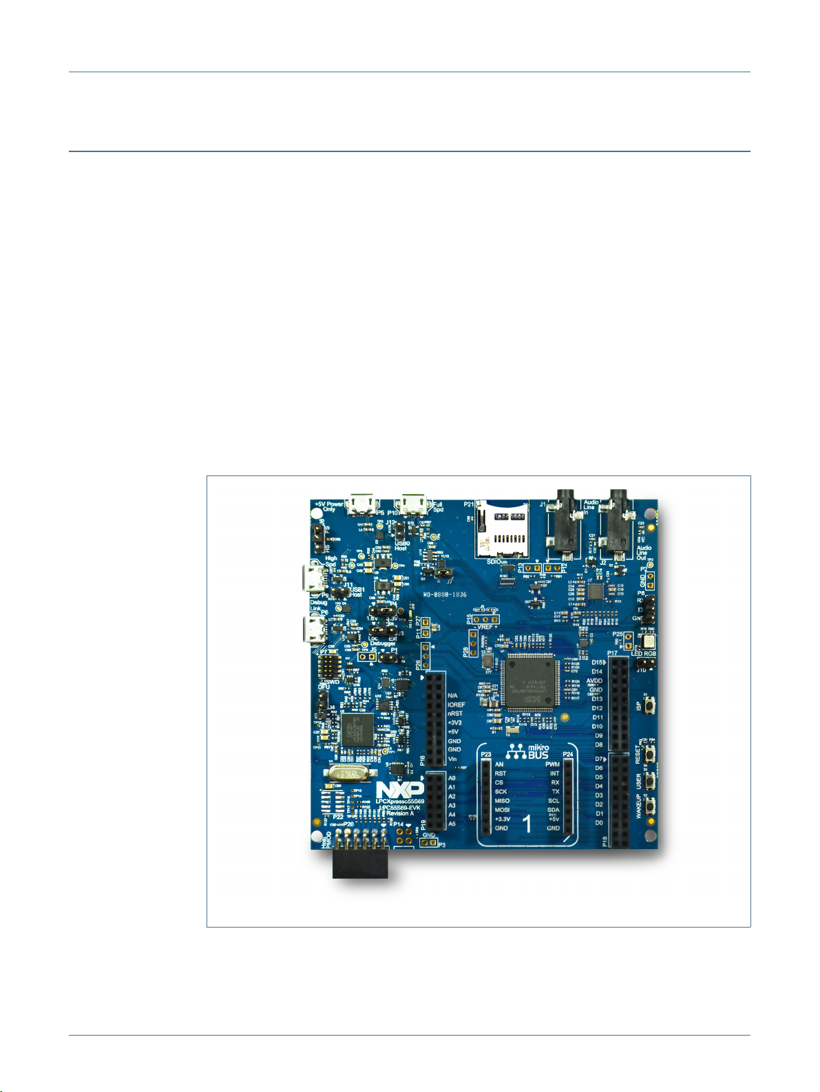
Workbench. The LPCXpresso55S69 board (order code LPC55S69-EVK) and
LPCXpresso55S28 board (order code LPC55S28-EVK) are the evaluation and
development platforms for the LPC55S6x and LPC55S2x/LPC552x families of MCUs
respectively.
See https://www.nxp.com/demoboard/LPC55S69-EVK or
https://www.nxp.com/demoboard/LPC55S69-EVK for more information on these boards,
including tutorial videos, development software and board hardware design files. Both
board designs are identical except for the LPC target MCU fitted; the information in this
manual applies to both board types unless otherwise noted. The abbreviation LPC55Sxx
is used to collectively refer to the LPC55S69 or LPC55S28 device on these boards. Note:
the schematics for this board indicate components that are not installed by default
with a red cross.
UM11158
LPCXpresso55S69/55S28 Development Boards
Fig 1. LPCXpresso55S69
The LPCXpresso55S69 and LPCXpresso55S28 boards include the following features:
• LPC55S69 Dual Cortex-M33 core processor or LPC55S28 Cortex-M33 processor
UM11158 All information provided in this document is subject to legal disclaimers. © NXP B.V. 2019. All rights reserved.
User manual Rev. 1.3 — 30 October 2019 3 of 23
Page 4

NXP Semiconductors
• Onboard, high-speed USB, Link2 debug probe with CMSIS-DAP and SEGGER J-Link
• UART and SPI port bridging from LPC55Sxx target to USB via the onboard debug
• Optional external debug probes with trace option (10 or 20 pin Cortex-M connectors)
• RGB user LED
• Reset, ISP, User/Wakeup and user buttons
• Multiple Expansion options, including Arduino UNO, Mikroe Click and PMod
• Micro SD card slot
• NXP MMA8652FCR1 accelerometer
• Stereo audio codec with line in/out
• High / full speed USB port with micro A/B connector for the host or device functionality
UM11158
LPCXpresso55S69/55S28 Development Boards
protocol options
probe
Reset button
UM11158 All information provided in this document is subject to legal disclaimers. © NXP B.V. 2019. All rights reserved.
User manual Rev. 1.3 — 30 October 2019 4 of 23
Page 5
NXP Semiconductors
2. Board layout and Settings
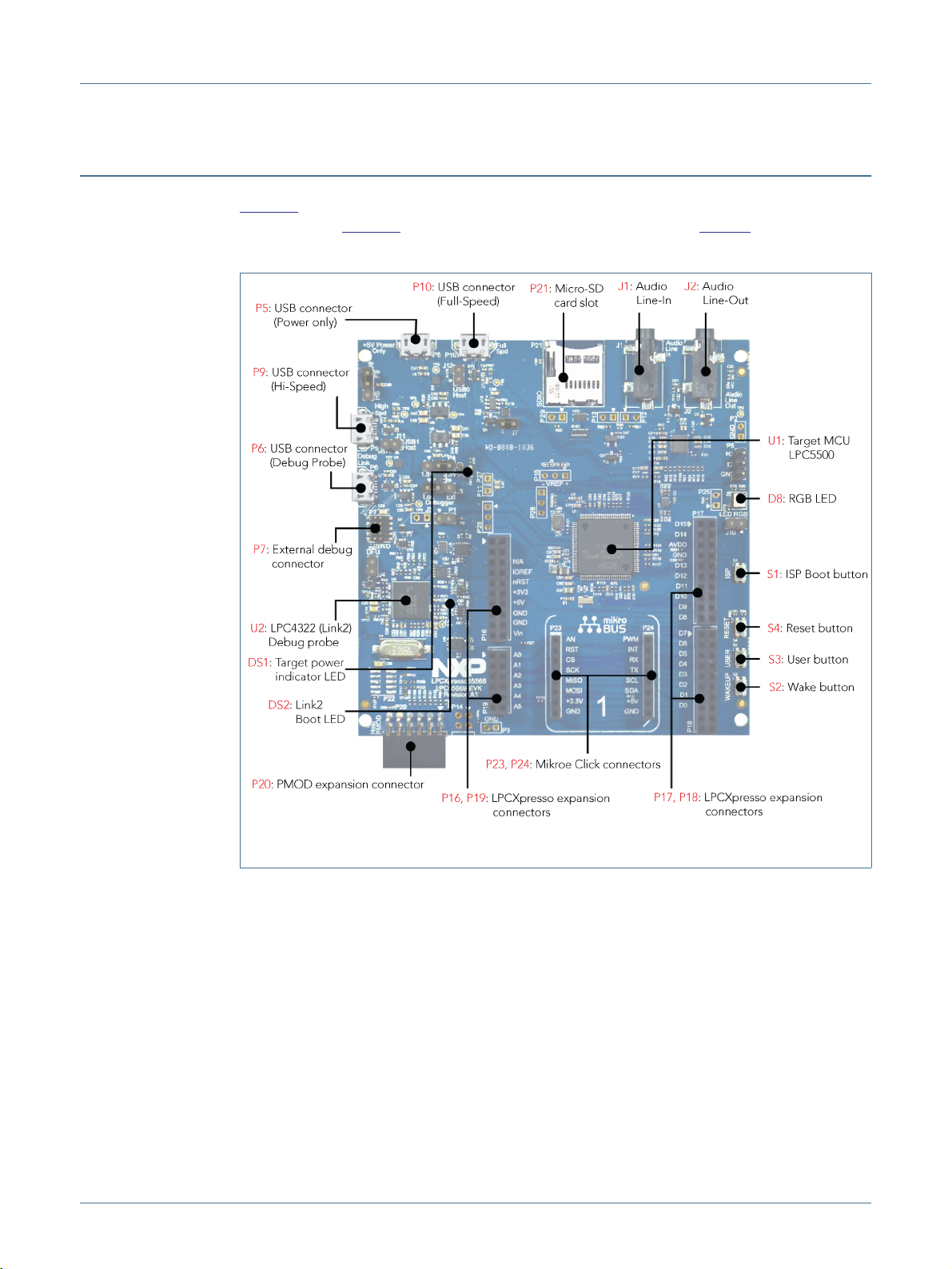
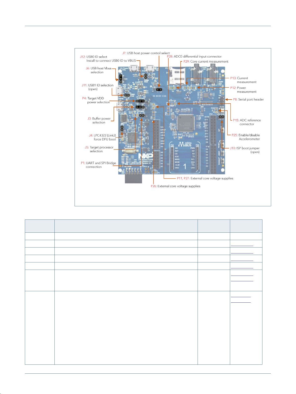
Figure 2 shows the layout of the board (top side), indicating location of the connectors and
buttons, while Figure 3 shows locations of jumpers and headers. Table 1 provides a
description of connectors, jumpers, LEDs and buttons.
UM11158
LPCXpresso55S69/55S28 Development Boards
Fig 2. Board connectors and buttons
UM11158 All information provided in this document is subject to legal disclaimers. © NXP B.V. 2019. All rights reserved.
User manual Rev. 1.3 — 30 October 2019 5 of 23
Page 6
NXP Semiconductors
UM11158
LPCXpresso55S69/55S28 Development Boards
Fig 3. Board jumpers and headers
Table 1. Indicators, buttons, connectors and LEDs
Circuit
reference
DS1 Target power indicator LED n/a n/a
DS2 Link2 boot LED n/a
D8 RGB User LED n/a Section 7.4
J1 Audio codec line input jack n/a Section 7.1
J2 Audio codec line output jack n/a Section 7.1
J3 Buffer Power Selection
J4 Link2 (LPC43xx) force DFU boot.
Description Default Reference
For On-board Target place in position 1-2 (default)
For Off-board Target place in position 2-3
Leave this jumper open (default) for Link2 to follow the normal boot
sequence. The Link2 will boot from internal flash if image is found
there. With the internal flash erased the Link2 normal boot sequence
will fall through to DFU boot.
Install this jumper to force the Link2 to DFU boot mode. Use this setting
to reprogram the Link2 internal flash with a new image (using the
LPCScrypt utility) or to use the MCUXpresso IDE with CMSIS-DAP
protocol.
Section 4.1
1-2
Open
Section 3.1,
Section 4.4
Section 3.,
Section 4.
Note that the Link2 flash is pre-programmed with a version of
CMSIS-DAP firmware by default.
UM11158 All information provided in this document is subject to legal disclaimers. © NXP B.V. 2019. All rights reserved.
User manual Rev. 1.3 — 30 October 2019 6 of 23
Page 7
NXP Semiconductors
LPCXpresso55S69/55S28 Development Boards
Table 1. Indicators, buttons, connectors and LEDs
Circuit
reference
J5 Target processor selection for the on-board Debug Probe.
J6 USB host Vbus selection
J7 USB host power control selection
J10 ISP boot jumper for LPC55Sxx. Installing this jumper ties port P0_5 to
J11 USB1 ID selection: USB1 ID is normally pulled to ground through a
J12 USB0 ID selection: USB1 ID is normally pulled to ground through a
P1 When open (default), the "Bridge" UART and SPI connections from the
P4 Target VDD power selection. For Revision A1 boards this jumper must
P5 External +5V power
P6 Link2 Debug Probe connector
P7 10 pin external debug probe / off board target connector
Description Default Reference
Jumper open (default) the LPC55Sxx Target SWD interface enabled.
Normal operating mode where the Target SWD is connected to either
the on-board Link2 Debug Probe or an external Debug Probe.
Jumper shunted, the LPC55Sxx Target SWD interface is disabled. Use
this setting only when the on-board Link2 Debug Probe is used to
debug an off-board target MCU.
Note that only one of USB0 or USB1 can be configured as a USB host
port at any given time (this is a board restriction, not a limitation of the
LPC55Sxx.)
Install jumper in position 1-2 for USB1 (High Speed) to provide Vbus
(i.e. enable USB host capability) (Default)
Install jumper in position 2-3 for USB0 (Full Speed) to provide Vbus (i.e.
enable USB host capability)
This jumper selects routing of USB port power and overcurrent detect
from either the USB0 or USB1 ports of the LPC55Sxx. Note that only
one of USB0 or USB1 can be configured as a USB host port at any
given time (this is a board restriction, not a limitation of the LPC55Sxx.)
Leave open when using USB1 (High Speed) as a USB host (Default)
Install jumper for USB0 (Full Speed) to provide Vbus (i.e. enable USB
host capability)
ground, forcing the LPC55Sxx into ISP mode whenever it is reset.
100Kohm resistor. Installing this jumper connects USB1 ID to VBUS.
100Kohm resistor. Installing this jumper connects USB0 ID to VBUS.
Link2 probe are driven to the LPC55Sxx target.
Install P1 when using the SPI interface at connector P20 and/or FC0
UART at P8. Note that this disables the Link2 SPI and UART (bridge)
connections.
be placed in the 3.3V position (2-3). An external supply voltage to the
LPC55Sxx can also be applied through pin 2 of this header
Micro USB connection for power to the LPC55Sxx target and peripheral
circuitry (excluding Link2 Debug Probe).
Micro USB type B connection for the on-board Link2 Debug Probe.
Note: do not use this connection when using an external Debug Probe.
This standard Cortex-M debug connector is used either to (1) connect
and off-board debug probe or (2) to connect an external debug target.
UM11158
Not installed Section 4.
1-2 (USB1) Section 6.1
Installed
(USB1)
Open Section 3.1,
Open Not required.
Open
Open
2-3 (3.3V) Section 5.
n/a Section 5.
n/a Section 4.
n/a Section 3.1.3
Section 6.1
Section 7.5.1
May be
removed in
future versions
Section 4.
UM11158 All information provided in this document is subject to legal disclaimers. © NXP B.V. 2019. All rights reserved.
User manual Rev. 1.3 — 30 October 2019 7 of 23
Page 8
NXP Semiconductors
UM11158
LPCXpresso55S69/55S28 Development Boards
Table 1. Indicators, buttons, connectors and LEDs
Circuit
reference
P8 Serial port header
P9 LPC55Sxx USB1 (high speed) micro AB port connector n/a Section 6.1
P10 LPC55Sxx USB0 (full speed) micro AB port connector n/a Section 6.1
P11, P26,
P27
P12 This header can be used to measure the voltage drop across a 2.43
P13 Current measurement header for LPC55Sxx. This header is in line with
P14 Host header for LPC55Sxx reset control.
P15 ADC reference connector
P16-P19 LPCXpresso expansion connectors, including Arduino R3 compatible
P20 PMod expansion connector / Host interface connector
P21 SD card slot
P23, P24 Mikroe Click site
P25 A header may be added at P25 to provide a convenient way to
P28 ADC0 differential input connector. This header provides access to the
Description Default Reference
0.1” header providing convenient access to Flexcom 0 USART (the
USART used for ISP boot). When using this port install jumper P1 to
disable the Link2 connection to this port.
Headers for external core voltage supplies (not installed). Do not use
these headers unless instructed to do so by NXP.
ohm resistor connected in line with the LPC55Sxx VDD supply, and
hence measure current consumption.
the VDD supply of the LPC55Sxx, with a zero ohm resistor (R92)
installed in parallel with it. To measure supply current to the LPC55Sxx,
remove R92 and insert an ammeter between the pins of P13.
This header is provided for convenient connection of a reset control
input to the LPC55Sxx from an off-board host.
This header provides an access point to inject positive and negative
voltage references for the LPC55Sxx ADC.
An external positive reference may be connected to pin 1. Note that a
solder jumper / zero ohm resistor must be in position 2-3 on J8.
An external negative reference may be connected to pin 3. Note that a
solder jumper / zero ohm resistor must be in position 2-3 on J9.
site. Provides connectivity to SPI (high speed SPI), USART (Flexcom
2), I2C (Flexcom 4 and Flexcom 1), I2S (Flexcom 7), ADC0, GPIO and
PLU pins.
This connector provides access to the SPI (Flexcom 3) and I2C
(Flexcom 1) ports that support LPC55Sxx ISP mode, along with 2 GPIO
lines. When using the SPI port at this connector ensure jumper P1 is
installed to disable the connection to the Link2 debug probe.
8-bit, full size card slot connected to the LPC55Sxx SD0 interface.
Supports 3.3V operation only.
Provides connectivity to standard Mikroe Click connectors. Shares SPI,
ADC, I2C and USART connections with the P16-P19 expansion
connectors.
enable/disable the on-board accelerometer. If this header is used,
remove the zero ohm resistor R20, which is in parallel with this header.
ADC0 negative and positive inputs, plus a ground pin.
n/a
n/a n/a
Not installed
Not installed
Not installed n/a
VREFP=VDD
VREFN=GND
n/a
Not installed
n/a Section 7.2
n/a
Not installed Section 7.3
n/a See schematic
Section 6.2
Section 5.1
Section 5.1
See schematic
Section 8.
Section 8.
Section 8.
UM11158 All information provided in this document is subject to legal disclaimers. © NXP B.V. 2019. All rights reserved.
User manual Rev. 1.3 — 30 October 2019 8 of 23
Page 9

NXP Semiconductors
Table 1. Indicators, buttons, connectors and LEDs
Circuit
reference
S1 ISP/User button
S2 Wake/User button
S3 User button
S4 Reset button
Description Default Reference
When pressed, this button connect sport pin P0_5 to ground. Hold this
button down while pressing and releasing Reset (S4) to force the
LPC55Sxx into ISP mode. Port P0_5 may also be reconfigured as a
GPIO in user application code to enable this button to be used for other,
user-defined purposes. A 2.2k ohm pull up is used to pull P0_5 high
when the button is not pressed.
This button, when pressed, pulls P1_18 to ground. A 100K ohm pull up
to VDD is connected to P1_18.
This button, when pressed, pulls P1_9 to ground. A 100K ohm pull up
to VDD is connected to P1_9, and this port is also connected to pin 1 of
expansion connector P18.
When pressed, reset is applied to the LPC55Sxx, expansion connector
(Arduino reset) P16, the Mikroe Click site reset, and U14 (debug
connector P7 reset when debugging an off-board target).
UM11158
LPCXpresso55S69/55S28 Development Boards
n/a
n/a Section 7.5.2
n/a
n/a
Section 7.5.1
Section 7.5.2
Section 7.5.3
3. Getting started
This section describes how to first power up the board and then how to start a first debug
session using the MCUXpresso SDK. The board is pre-programmed with a simple
program indicating that the target MCU is running. Connect a micro USB cable from
connector P5 to a host computer or power supply to power-up the board and run this
program.
The following debug probes can be used with those development and the board (check
compatibility between debug probe and IDE used, including support for Arm Cortex M33
cores):
• On-board debug probe (LPC4322 “Link2”)
• LPC-Link2 (OM13054) debug probe from NXP or Embedded Artists
• SEGGER J-link probes (version 9 and newer). Ensure driver version 6.44a or later is
• P&E Micro probes
• Keil ULINK2 probes
• IAR I-Jet probes
Other debug probes may also be supported by IAR and Keil tools and by other
IDEs/debug tools; refer the websites of these companies for further information.
installed.
3.1 Starting a debug session using the on-board (Link2) Debug Probe
By default, the Board is configured to use the on-board Debug Probe (Link2) to debug the
on-board target (LPC55Sxx), using the CMSIS-DAP debug protocol pre-programmed into
the Link2 Flash memory. The MCUXpresso IDE or other development tools that support
UM11158 All information provided in this document is subject to legal disclaimers. © NXP B.V. 2019. All rights reserved.
User manual Rev. 1.3 — 30 October 2019 9 of 23
Page 10

NXP Semiconductors
the CMSIS-DAP protocol can be used in the default configuration. Check with your
toolchain vendor for availability of specific device support packs for the LPC55Sxx series
devices.
Note that when using the MCUXpresso IDE, the on-board Link2 can also be booted in
DFU mode by installing a jumper on J4; if this is done then the IDE will download
CMSIS-DAP to the probe as needed. Using DFU boot mode will ensure that the most
up-to-date / compatible firmware image is used with the MCUXpresso IDE.
NOTE: if the Debug Probe is set up to boot in DFU mode, the USB bridge functions
(virtual COM port) and Debug Probe features will not be available if the board is not first
initialized by the MCUXpresso IDE.
3.1.1 Installation steps for use with MCUXpresso IDE
Download and install the MCUXpresso IDE.
Configure and download an SDK package (with the MCUXpresso IDE tool chain option
selected) from the MCUXpresso SDK Builder utility (http://mcuxpresso.nxp.com).
Recommended: Install J4 to force the Link2 Debug Probe to boot in DFU mode (see notes
above).
UM11158
LPCXpresso55S69/55S28 Development Boards
Ensure jumper -- is fitted in position -- (local target powered), and -- is not installed (target
SWD enabled). These are the default positions set during board manufacture.
Connect the board to the USB port of your host computer, connecting a micro USB cable
to connector P6. The board will boot and run the pre-installed demo.
Allow about 10 seconds for the LPCXpresso55S69/S28 Board to enumerate for the first
time; the device will appear as "LPC Device".
If the first attempt to debug a project fails in the IDE, cancel the debug session and
repower the board. On some machines the drivers take longer to enumerate for the first
time, so these steps should correct this issue.
The board is now ready to be used with the MCUXpresso SDK examples for the
LPCXpresso55S69/55S28.
When the board is used for the first time, it is recommended to force the LPC55Sxx target
into a known state by performing an ISP boot before attempting to run your first example
code. This can be achieved by pressing and holding down the ISP button while pressing
and releasing the reset button or installing the LPC55Sxx ISP jumper.
3.1.2 Installation steps to use Keil and IAR tools with on-board debug probe
Download and install LPCScrypt (https://www.nxp.com/lpcscrypt). This will install required
drivers for the board. Note that the Link2 (LPC4322 device) is pre-programmed with
CMSIS-DAP firmware. If you have previously installed LPCScrypt please ensure version
2.1 or later is installed.
Ensure jumper J3 is fitted in position 1-2 (local target powered), and J5 is not installed
(target SWD enabled). These are the default positions set during board manufacture.
UM11158 All information provided in this document is subject to legal disclaimers. © NXP B.V. 2019. All rights reserved.
User manual Rev. 1.3 — 30 October 2019 10 of 23
Page 11

NXP Semiconductors
The Link2 Debug Probe on the board will have been programmed with CMSIS-DSP
firmware during manufacture, but can also be updated with J-link OB for LPC-Link2. To
start the board with this firmware running, ensure J4 is not installed as power is
connected, so the Link2 Debug Probe boots from internal flash. If you wish to
update/change the Link2 firmware please follow the steps described in
Connect the Board to the USB port of your host computer, connecting a micro USB cable
to connector P6 ("Debug-Link"). The board will boot and run the pre-installed demo. Allow
about 30 seconds for the Link2 devices to enumerate for the first time. It is not necessary
to check the Hardware Manager on your host computer, however if this is done there will
be five devices (if using CMSIS-DAP protocol); four under Human Interface Devices
(CMSIS-DAP, LPC-SIO, two HID Compliant Devices, and a USB Input Device) and one
under Ports (LPC-LinkII Ucom.)
Your board is now ready to use with your 3rd party tool. Follow the instructions for those
tools for using a CMSIS-DAP probe. MCUXpresso IDE can also be used with the board
after setting up the board this way.
When the board is used for the first time, it is recommended to force the target into known
state by performing an ISP boot before attempting to run your first example code. This can
be achieved by pressing and holding down the ISP button while pressing and releasing
the reset button.
UM11158
LPCXpresso55S69/55S28 Development Boards
Section 4.2.
3.1.3 Starting a debug session using an external Debug Probe
Code running on the LPC55Sxx target can be debugged using an external Debug Probe
that conforms to the standard ARM Cortex-M debug connector. To use an external Debug
Probe connect the probe to the SWD connector (P7) and connect power via the micro
USB connector P5.
Note: The Debug link USB connector P6 must be left unconnected so that the Link2
Debug Probe is left unpowered and does not contend with the SWD interface signals from
the external Debug Probe. Also note that the VCOM function provided by the on-board
Debug Probe is not available when using an external debug probe.
UM11158 All information provided in this document is subject to legal disclaimers. © NXP B.V. 2019. All rights reserved.
User manual Rev. 1.3 — 30 October 2019 11 of 23
Page 12

NXP Semiconductors
4. On-board (Link2) Debug probe
This section describes the features provided by the on-board Link2 Debug Probe,
including how to use this to debug an exernal target.
The Link2 Debug Probe is implemented using an LPC432x MCU (circuit reference U2),
which provides a high speed USB port interface to the host computer that runs the
development tools. This device is not intended for developer use, and should only be used
with approved firmware images from NXP. The Link2 on-chip flash memory is factory
programmed with a firmware image that supports CMSIS-DAP debug protocol, but also
includes other USB end point functions:
• Virtual COM (VCOM) port: a serial device that can be used with any host computer
application design for serial port communication (e.g. Teraterm, puTTY, etc.) Set the
terminal program for baud rate to 115200, no parity, 8 bit data, 1 stop bit, no flow
control.
• SWO trace end point: this virtual device is used by MCUXpresso to retrieve SWO
trace data. See the MCUXpresso IDE documentation for more information.
• I2S/SPI bridges: bridge device from I2C and SPI ports of the LPC target.
UM11158
LPCXpresso55S69/55S28 Development Boards
All of these devices are independent of each other and of the CMSIS-DAP debug device
that is enumerated when the board is connected to a host computer; for example, the
VCOM port can be used if the board is running an application when no debugger is
running.
In order to correctly install and use the Link2 device on the LPCXpresso55S69 (required
for any debugging purpose) for Windows 7 or 8 host computers, install the drivers first.
These drivers will automatically be installed when MCUXpresso IDE has already been
installed. If these IDEs are not being used, it is recommended LPCScrypt be installed as
this also includes the required drivers. All these tools and utilities are available for free
download at https://www.nxp.com/lpcscrypt.
The CMSIS-DAP firmware image installed at the factory (and by LPCScrypt) will uniquely
identify itself to the host computer so that more than one board can be connected to that
host computer at any time. Some toolchains cannot discern between multiple debug
devices; refer to your toolchain documentation for more information (note the
MCUXpresso IDE does support multiple LPCXpresso board targets.)
Note: The Link2 only boots when the board is power cycled; the reset button on the board
does not reset the Link2.
When using MCUXpresso IDE, the Link2 can be automatically booted with the latest /
most appropriate firmware for that IDE version by installing J4 (DFU jumper) before
powering up the board. This is the recommended approach for the MCUXpresso IDE.
Note that if J4 is installed when powering the board then the VCOM port (and other
devices mentioned above) device will not appear until the MCUXpresso IDE boots the
Debug Probe. The Debug Probe is booted once a debug session is started (that is, the
IDE attempts to download code to the target).
UM11158 All information provided in this document is subject to legal disclaimers. © NXP B.V. 2019. All rights reserved.
User manual Rev. 1.3 — 30 October 2019 12 of 23
Page 13

NXP Semiconductors
4.1 Link2 boot LED
LED DS2 is the Link2 MCU BOOT0_LED indicator. This LED reflects the state of Link2
MCU pin P1_1. When the boot process fails, DS2 will toggle at a 1 Hz rate for 60
seconds. After 60 seconds, the Link2 MCU is reset.
4.2 Programming the Link2 firmware
As mentioned earlier in this section, it is not normally necessary to program the Link2
firmware. However, this can easily be accomplished using the supporting utility,
LPCScrypt.
To program the Link2 Flash the Link2 device (LPC432x) must be in DFU mode. If the
Link2 already has a valid image in the flash, it will need to be forced into DFU mode by
placing a jumper shunt on J4 (DFU), and power cycling (disconnecting then reconnecting
power via P6.) Link2 MCU programming is performed using the LPCScrypt utility (see
http://www.nxp.com/lpcscrypt). Instructions for using the tool are located at the same web
page
After installing LPCScrypt, use either the “Program LPC-Link2 with CMSIS-DAP” or
“Program LPC-Link2 with JLink” utilities provided in that installation to update the
firmware, following on-screen instructions.
UM11158
LPCXpresso55S69/55S28 Development Boards
4.3 VCOM port
The identifier of the VCOM port will vary between boards and hosts as each board will
enumerate with a unique identifier. On Windows, to determine the COM port, open the
Windows operating system Device Manager. This can be achieved by going to the
Windows operating system Start menu and typing “Device Manager” in the search bar. In
the device manager look under “Ports”; the LPC-LinkII UCom Port device and its name
should be visible. NOTE: this VCOM port will only appear if (a) the Debug Probe has been
programmed with the CMSIS-DAP firmware and the Debug Probe DFU link (J4) is
removed at power up, or (b) if the Debug Probe has been configured for DFU boot (J4
installed) at power up and MCUXpresso IDE has booted it (by starting a debug session.)
If the J-Link firmware image has been programmed into the Debug Probe and DFU boot
mode is not being used, then a VCOM device called Jlink CDC UART port will appear
instead of the LPC-LinkII UCom port.
Note that the VCOM port is not available when the Link2 Debug Probe is not powered.
4.4 Configuring the LPCXpresso55S69 to debug an off-board target
The LPCXpresso55S69 board’s Link2 Debug Probe may be used to debug an off-board
target MCU. The on-board Link2 Debug Probe is capable of debugging target MCU’s with
a VDDIO range of 1.6V to 3.6V. To keep the on-board target LPC55Sxx MCU from
interfering with the SWD interface, J5 must be fitted (note: the header for this jumper is not
installed during board production). The Link2 Debug Probe SWD should be connected by
a ribbon cable between the P1 connector to the off-board target MCU SWD interface.
Power the LPCXpresso55S69 board from the Link USB connector P6, and fit jumper J3
across pins 2 - 3 (External Target).
UM11158 All information provided in this document is subject to legal disclaimers. © NXP B.V. 2019. All rights reserved.
User manual Rev. 1.3 — 30 October 2019 13 of 23
Page 14

NXP Semiconductors
5. Board Power
The LPCXpresso55S69 board requires +5V input to power the on-board voltage low
dropout linear regulators, of which there are 3, all available from Torex Semiconductor.
The Link2 Debug probe has a 2.5V regulator (U10) which draws power from USB
connector P6 (“Debug Link”) only. The Debug Probe is unpowered if P6 is unconnected.
There are two other regulators, providing the option of 1.8V (U8) or 3.3V (U9) to the other
devices on the board; these regulators can be powered by any of the following (+5V)
sources:
• USB +5V Power only connector (P5)
• USB Full Speed connector for LPC55Sxx (P10)
• USB High Speed connector for LPC55Sxx (P9)
• USB Debug Link connector (P6)
The +5V sources above are connected via protection diodes to prevent reverse powering
of any of them by another source. The +5V output of these combined sources is also
connected to the Arduino and Mikroe expansion sites. Note that if P9 or P10 is configured
as a USB host port then those connectors will not supply power to the board and another
source must be provided.
UM11158
LPCXpresso55S69/55S28 Development Boards
LPCXpresso55S69 Revision A1 boards (with LPC55S69 revision 0A silicon) require a
minimum supply voltage of 1.85V, so jumper P4 must be set in the 3.3V position, or an
external supply provided to the center pin of P4. For Revision A2 (or later)
LPCXpresso55S69 boards and all LPCXpresso55S28 boards P4 may be set in the 1.8V
or 3.3V position.
Note that the MMA8652 Accelerometer and use of most SD cards requires the board to
be configured for 3.3V operation. The power connection to the Accelerometer may be
disconnected by removing R20; installing header P25 provides a convenient way to
connect/disconnect this.
For further details, refer to the board schematics.
5.1 Measuring LPC55Sxx device supply current
Current supply to the LPC55Sxx Core can be measured via P29 (supply into VDDA and
the on-board DC-DC converter) by removing R85. Supply current into the entire device
(VDDA, DC-DC and I/O) can be measured via P13 (removing R92), or by measuring the
voltage drop across the 2.43 ohm resistor (R91) which is accessible at P12.
6. Board serial connections
This section describes connections between LPC55Sxx on-board serial peripherals and
connectors for use with off-board devices.
UM11158 All information provided in this document is subject to legal disclaimers. © NXP B.V. 2019. All rights reserved.
User manual Rev. 1.3 — 30 October 2019 14 of 23
Page 15

NXP Semiconductors
6.1 LPC55Sxx USB Ports
The Board incorporates micro AB connectors for both of USB0 (Full Speed, connector
P10) and USB1 (High Speed, connector P9) ports of the LPCXpresso55S69. Both of
these ports are capable of operating as a device or a host, and this is why micro AB
connectors are used.
The Board can only be configured to support one of these ports as a host at a time (this is
a limitation of the board, not the LPC55Sxx). When either port is used as a host, power
must be supplied to the board via the +5V power only micro B USB port. Jumper J6 is
used to connect power from a load switch to the VBUS signal of the port selected; J6
should be placed in position 1-2 for USB1 or position 2-3 for USB0. If neither USB port is
being used as a USB host this jumper is not required.
6.2 USART header
Header P8 is provided as a convenient way to use an LPC55Sxx USART with a serial to
USB cable. Flexcom 0 ports (P0_29 and P0_30) are used for this feature, since these
ports are assigned for USART ISP mode. Note that these ports are shared with the Link2
debug probe (LPC4322) and PMod connector; when using this header ensure that there
is no conflicting device connected to the PMod connector and that jumper P1 is installed
to disable the connection to the Link2. Always ensure the serial cable is only connected
when the board is powered to prevent the LPC55S69 being powered through this
TXD/RXD pins. Note that there is no level shifter between the LPC55Sxx target and this
header, so a UART to serial cable with voltage levels matching the setting of the P4 power
supply voltage selection jumper must be used.
UM11158
LPCXpresso55S69/55S28 Development Boards
7. On-board peripherals
This section describes how the on-board peripheral devices of the Board are connected to
the LPC55Sxx and relevant configuration options. For full details of these devices please
refer to the individual device datasheets. For circuit further details, refer to the board
schematics.
7.1 Audio Codec
The LPCXpresso55S69 board incorporates a Cirrus Logic (Wolfson) WM8904 audio
codec. This codec has both I2C (for control) and I2S (for data) interfaces.
The I2C interface of the codec is routed to Flexcomm 4 of the LPC55Sxx, the same
connection as used for the other I2C devices on the board; the Codec has an address of
0b0011010.
The Flexcomm 6 and Flexcomm 7 interfaces of the LPC55Sxx are connected respectively
to the Codec for data sent to / receive from the Codec. The board design assumes pad
sharing between Flexcom 6 and Flexcom 7 for I2S connections.
Table 2. Audio Codec port connections
Circuit reference Port Flexcoms
I2S SCK P0_21 Flexcom 6 & 7, pad shared
I2S TX/RX Data P0_20 Flexcom 6 & 7, pad shared
UM11158 All information provided in this document is subject to legal disclaimers. © NXP B.V. 2019. All rights reserved.
User manual Rev. 1.3 — 30 October 2019 15 of 23
Page 16

NXP Semiconductors
Table 2. Audio Codec port connections
Circuit reference Port Flexcoms
I2S WS P0_19 Flexcom 6 & 7, pad shared
I2C SDA P1_21 Flexcom 4
I2C SCL P1_20 Flexcom 4
I2S connections from the LPC55Sxx are also connected to the Expansion connectors;
solder jumpers may be removed to disconnect the on-board codec if an external I2S
device is to be used instead.
Line input (J1) and line output (J2) 1/4” stereo jack sockets provide analog I/O
connections to the Codec. See schematic for further information.
7.2 Micro SD card slot
The micro SD card (P21) included in the LPCXpresso55S69 board provides a 4-bit SDIO
interface to support memory cards, plug-in WiFi modules, etc. Power enable to the socket
is provided via transistor enabled by P1_0.
Software drivers and related examples for the SD card are provided as part of the
MCUXpresso SDK.
Table 3. Micro SD card connections
SDIO interface signals Port Notes
SDIO Clock P0_7 IOCON function 2
SDIO Command P0_8 IOCON function 2
D0 P0_9 IOCON function 2
D1 P0_17 IOCON function 2
D2 P0_24 IOCON function 2
D3 P0_25 IOCON function 2
Card detect P0_21 IOCON function 2
Power enable P1_0 GPIO. Active low.
UM11158
LPCXpresso55S69/55S28 Development Boards
7.3 Accelerometer
The board includes an NXP MMA8652FCR1 accelerometer, interfaced to Flexcom 4
(ports P1_21 and P1_20) with its interrupt output connected to P1_19 (this signal is also
shared with the Expansion connector P18 via a 100 ohm resistor (R5).) The
accelerometer has an I2C address of 0b0011101.
Note that the accelerometer can only be used when the board is configured for 3.3V
operation. Resistor R20 may be removed to disconnect the MMA8652 from the supply
rail, and P25 may be installed to provide a convenient way to connect/disconnect it to/from
power.
Resistors R3 and R4 are zero ohm links, provided to enable the MMA8652 to be
disconnected from P1_20 and P1_21 to avoid leakage effects when the board is
configured for 1.8V operation.
I2C software drivers are provided as part of the MCUXpresso SDK, and example code is
provided to illustrate how to read values from the accelerometer.
UM11158 All information provided in this document is subject to legal disclaimers. © NXP B.V. 2019. All rights reserved.
User manual Rev. 1.3 — 30 October 2019 16 of 23
Page 17

NXP Semiconductors
7.4 RGB User LED
An User controlled RGB LED is provided on the Board, located on the right hand edge.
The LEDs in this device are controlled by LPC55Sxx ports P1_4 (Blue), P1_6 (Red), P1_7
(Green) with the LEDs being illuminated when the respective LED is pulled low. Note that
these port lines are also connected to expansion connector P18.
7.5 Buttons
Four buttons are provided on the LPCXpresso55S69, as described in this section.
7.5.1 ISP (S1)
P0_5 is pulled up to VDD via a 2.2 kohm resistor; pressing this button will pull P0_5 low.
This port is read by the LPC55Sxx boot code to determine if the MCU should enter In
System Programming (ISP) mode. The main purpose of this button is to force the
LPC55Sxx into ISP mode at boot time; to do this hold down this button while pressing and
releasing the Reset button, or while connecting power to the board. While the main
purpose of ISP mode is to program the flash of the LPC55Sxx, forcing the MCU into this
mode places it into a known state in which development tools can gain debug control. If an
application in flash is crashing or disabling the SWD port unintentionally, then ISP mode
can be useful to recover control of the board. Refer to the LPC55S6x/S2x/2x User Manual
for more information on ISP mode.
UM11158
LPCXpresso55S69/55S28 Development Boards
The ISP button can also be used in user application code. Care should be taken if P0_5 is
configured as an output driving high, since pressing this button will short it to ground.
Note that jumper J10 may also be used as a convenient way to always assert ISP when
the LPC55Sxx is reset or powered up. This jumper is in parallel with S1.
7.5.2 User (S3) and Wake (S2) buttons
The User (S3) and Wake (S2) buttons are intended for user application use. These
buttons pull ports P1_9 (User) and P1_18 (Wake) low when the button is pressed.
100kohm resistors are used to pull these two ports to VDD then the buttons are not
pressed.
7.5.3 Reset
Pressing this button will assert reset to the LPC55Sxx and to the Mikroe and Arduino
connector sites. Note that the Debug Probe (LPC4322) is not reset when this button is
pressed.
8. Expansion connectors
The LPCXpresso55S69 includes 3 expansion connector sets, incorporating support for
Arduino UNO R3, Mikroe Click and PMod standards. The Arduino UNO connector
footprint is surrounded by additional connectors that are compatible with other
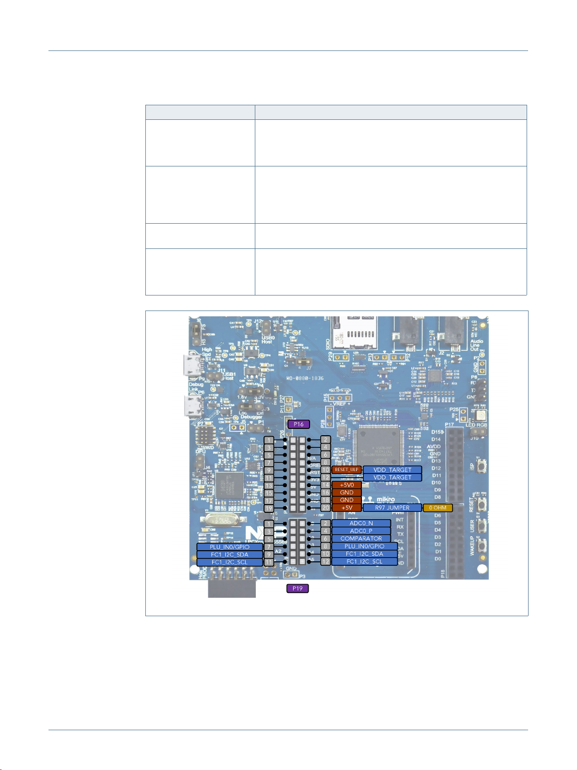
LPCXpresso V3 boards. Pin out diagrams are provided below in Figure 4 and Figure 5.
For further details, refer to the board schematics.
8.1 Mikroe Click Site
The connectors P23 and P24 provide a Mikroe Click module site for the wide range of
UM11158 All information provided in this document is subject to legal disclaimers. © NXP B.V. 2019. All rights reserved.
User manual Rev. 1.3 — 30 October 2019 17 of 23
Page 18

NXP Semiconductors
add-on modules available from MikroElektronika. Note that this site shares the same SPI,
I2C and UART connections as the Arduino/LPCXpresso V3 expansion connectors.
8.2 Host / PMod Connector
Connector P20 is a optional connector (not installed by default) which can provide
convenient access for a remote host to the SPI and I2C ports of the LPC55Sxx that
support ISP mode. When setting up the Board to be used with a host, jumper P1 must be
installed to prevent conflict with the Link2 (which can also emulate an SPI or I2C host).
Jumper J4 can be used to force the LPC55Sxx to boot in ISP mode, and connector P14
can be installed and used to provide an external reset control input from the host, The
connector footprint and connection can also be used to connect to external PMod
peripherals that follow the PMod I2C, or SPI (Type 2 or 2A) standards. Refer to the PMod
specifications from Digilent Inc. for more information.
Table 4. Micro SD card connections
SDIO interface signals Port Notes
SDIO Clock P0_7 IOCON function 2
SDIO Command P0_8 IOCON function 2
D0 P0_9 IOCON function 2
D1 P0_17 IOCON function 2
D2 P0_24 IOCON function 2
D3 P0_25 IOCON function 2
Card detect P0_21 IOCON function 2
Power enable P1_0 GPIO. Active low.
UM11158
LPCXpresso55S69/55S28 Development Boards
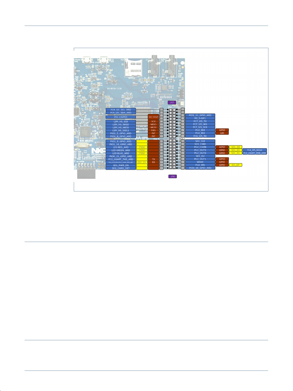
8.3 Arduino and LPCXpresso V3 expansion connectors
The connectors P16-P19 provide Arduino UNO R3 compatibility and access to several
other signals for use in prototyping. The overall footprint is compatible with the
LPCXpresso V3 expansion connector footprint used on other LPCXpresso boards of this
type. Note that some ports used on these connectors are shared with other
devices/connectors on the board, including the Mikroe Click site, audio codec and RGB
LED. Refer to the schematic for further information.
When using an Arduino shield with the Board, align P17 of the Arduino shield (SCL) with
pin 1 of connector P17 on the LPCXpresso55S69 board.
UM11158 All information provided in this document is subject to legal disclaimers. © NXP B.V. 2019. All rights reserved.
User manual Rev. 1.3 — 30 October 2019 18 of 23
Page 19
NXP Semiconductors
Table 5. Micro SD card connections
Expansion connector Port
P17 The odd number pins are compatible with Arduino Uno rev3 Digital
P18 The odd numbered pins 1 – 15 are compatible with Arduino Uno rev3
P16 The even numbered pins 6 – 20 are compatible with the Arduino Uno
P19 The even numbered pins 2 – 12 are compatible with Arduino Uno
UM11158
LPCXpresso55S69/55S28 Development Boards
15:8, AREF, SDA & SCL connector. The even numbered pins are
used for external access and expansion of LPC55Sxx signals not
used by the Arduino Uno rev3 compatible interface.
Digital 7:0 connector. The even numbered pins, and odd numbered
pins 17 and 19, are used for external access and expansion of
LPC55Sxx signals not used by the Arduino Uno rev3 compatible
interface.
rev3 Power connector standard.
rev3 Analog connector. The odd numbered pins are used for external
access and expansion of LPC55Sxx signals not used by the Arduino
Uno rev3 compatible interface.
Fig 4. P16 and P19 connector pinouts
UM11158 All information provided in this document is subject to legal disclaimers. © NXP B.V. 2019. All rights reserved.
User manual Rev. 1.3 — 30 October 2019 19 of 23
Page 20
NXP Semiconductors
UM11158
LPCXpresso55S69/55S28 Development Boards
SDIO port 1 of the LPC55Sxx is routed to the expansion connector to provide access to
this interface. Note that the power enable signal used for this SDIO interface is not one of
the port pins that supports in SD1_POWER_EN function; this because all port pins that
support this function are required for other features of the board. PIO1_16 is used instead
for the power enable function, configured as a GPIO.
9. Board Power
This section describes miscellaneous board features that we not covered elsewhere in
this manual.
9.1 LPC55Sxx ADC references and inputs
By default, the LPC55Sxx ADC positive reference is connected to VDDA and the negative
reference to ground. Different reference voltages may be used by moving the zero ohm
link J8 or J9 (for positive or negative reference respectively) from the 1-2 to the 2-3
position, and connecting an external reference to P15 (pin 1 for positive, pin 3 for
negative).
An external differential ADC input signal can be applied at P28 or at the P19 expansion
connector. This connection is routed to PIO0_16 and PIO0_23.
Fig 5. P17 and P18 connector pinouts
10. Notes on LPCXpresso55S69 Revision A1 boards
Initial production LPCXpresso55S69 boards, marked as Revision A1, use LPC55S69
revision 0A silicon. Please refer to errata documentation from NXP for full details of device
errata (https://www.nxp.com/docs/en/errata/ES_LPC55S6x.pdf)
UM11158 All information provided in this document is subject to legal disclaimers. © NXP B.V. 2019. All rights reserved.
User manual Rev. 1.3 — 30 October 2019 20 of 23
Page 21

NXP Semiconductors
11. Board operating conditions
These boards have been designed for use in laboratory conditions (0 to 50 degrees
Celsius) and should not be used for extended temperature testing. Refer to the data sheet
of the LPC55xx MCU being used for full operating conditions for that device.
UM11158
LPCXpresso55S69/55S28 Development Boards
UM11158 All information provided in this document is subject to legal disclaimers. © NXP B.V. 2019. All rights reserved.
User manual Rev. 1.3 — 30 October 2019 21 of 23
Page 22

NXP Semiconductors
UM11158
LPCXpresso55S69/55S28 Development Boards
12. Legal information
12.1 Definitions
Draft — The document is a draft version only. The content is still under internal review and subject to formal approval, which may result in modifications or
additions. NXP Semiconductors does not give any representations or warranties as to the accuracy or completeness of information included herein and shall
have no liability for the consequences of use of such information.
12.2 Disclaimers
Limited warranty and liability — Information in this document is believed to be accurate and reliable. However, NXP Semiconductors does not give any
representations or warranties, expressed or implied, as to the accuracy or completeness of such information and shall have no liability for the consequences of
use of such information.
In no event shall NXP Semiconductors be liable for any indirect, incidental, punitive, special or consequential damages (including - without limitation - lost profits,
lost savings, business interruption, costs related to the removal or replacement of any products or rework charges) whether or not such damages are based on
tort (including negligence), warranty, breach of contract or any other legal theory.
Notwithstanding any damages that customer might incur for any reason whatsoever, NXP Semiconductors’ aggregate and cumulative liability towards customer
for the products described herein shall be limited in accordance with the Terms and conditions of commercial sale of NXP Semiconductors.
Right to make changes — NXP Semiconductors reserves the right to make changes to information published in this document, including without limitation
specifications and product descriptions, at any time and without notice. This document supersedes and replaces all information supplied prior to the publication
hereof.
Suitability for use — NXP Semiconductors products are not designed, authorized or warranted to be suitable for use in life support, life-critical or safety-critical
systems or equipment, nor in applications where failure or malfunction of an NXP Semiconductors product can reasonably be expected to result in personal
injury, death or severe property or environmental damage. NXP Semiconductors accepts no liability for inclusion and/or use of NXP Semiconductors products in
such equipment or applications and therefore such inclusion and/or use is at the customer’s own risk.
Applications — Applications that are described herein for any of these products are for illustrative purposes only. NXP Semiconductors makes no representation
or warranty that such applications will be suitable for the specified use without further testing or modification.
Customers are responsible for the design and operation of their applications and products using NXP Semiconductors products, and NXP Semiconductors
accepts no liability for any assistance with applications or customer product design. It is customer’s sole responsibility to determine whether the NXP
Semiconductors product is suitable and fit for the customer’s applications and products planned, as well as for the planned application and use of customer’s third
party customer(s). Customers should provide appropriate design and operating safeguards to minimize the risks associated with their applications and products.
NXP Semiconductors does not accept any liability related to any default, damage, costs or problem which is based on any weakness or default in the customer’s
applications or products, or the application or use by customer’s third party customer(s). Customer is responsible for doing all necessary testing for the
customer’s applications and products using NXP Semiconductors products in order to avoid a default of the applications and the products or of the application or
use by customer’s third party customer(s). NXP does not accept any liability in this respect.
Export control — This document as well as the item(s) described herein may be subject to export control regulations. Export might require a prior authorization
from national authorities.
12.3 Trademarks
Notice: All referenced brands, product names, service names and trademarks are the property of their respective owners.
UM11158 All information provided in this document is subject to legal disclaimers. © NXP B.V. 2019. All rights reserved.
User manual Rev. 1.3 — 30 October 2019 22 of 23
Page 23

NXP Semiconductors
LPCXpresso55S69/55S28 Development Boards
13. Contents
1 Introduction . . . . . . . . . . . . . . . . . . . . . . . . . . . . 3
2 Board layout and Settings . . . . . . . . . . . . . . . . 5
3 Getting started . . . . . . . . . . . . . . . . . . . . . . . . . . 9
3.1 Starting a debug session using the on-board (Link2) Debug Probe 9
3.1.1 Installation steps for use with MCUXpresso IDE 10
3.1.2 Installation steps to use Keil and IAR tools with on-board debug probe 10
3.1.3 Starting a debug session using an external Debug Probe 11
4 On-board (Link2) Debug probe. . . . . . . . . . . . 12
4.1 Link2 boot LED . . . . . . . . . . . . . . . . . . . . . . . 13
4.2 Programming the Link2 firmware . . . . . . . . . . 13
4.3 VCOM port . . . . . . . . . . . . . . . . . . . . . . . . . . . 13
4.4 Configuring the LPCXpresso55S69 to debug an off-board target 13
5 Board Power. . . . . . . . . . . . . . . . . . . . . . . . . . . 14
5.1 Measuring LPC55Sxx device supply current . 14
6 Board serial connections . . . . . . . . . . . . . . . . 14
6.1 LPC55Sxx USB Ports . . . . . . . . . . . . . . . . . . . 15
6.2 USART header . . . . . . . . . . . . . . . . . . . . . . . 15
7 On-board peripherals . . . . . . . . . . . . . . . . . . . 15
7.1 Audio Codec . . . . . . . . . . . . . . . . . . . . . . . . . . 15
7.2 Micro SD card slot . . . . . . . . . . . . . . . . . . . . . 16
7.3 Accelerometer. . . . . . . . . . . . . . . . . . . . . . . . . 16
7.4 RGB User LED . . . . . . . . . . . . . . . . . . . . . . . . 17
7.5 Buttons . . . . . . . . . . . . . . . . . . . . . . . . . . . . . . 17
7.5.1 ISP (S1) . . . . . . . . . . . . . . . . . . . . . . . . . . . . . 17
7.5.2 User (S3) and Wake (S2) buttons. . . . . . . . . . 17
7.5.3 Reset . . . . . . . . . . . . . . . . . . . . . . . . . . . . . . . 17
8 Expansion connectors . . . . . . . . . . . . . . . . . . 17
8.1 Mikroe Click Site . . . . . . . . . . . . . . . . . . . . . . . 17
8.2 Host / PMod Connector . . . . . . . . . . . . . . . . . 18
8.3 Arduino and LPCXpresso V3 expansion connectors 18
9 Board Power. . . . . . . . . . . . . . . . . . . . . . . . . . . 20
9.1 LPC55Sxx ADC references and inputs. . . . . . 20
10 Notes on LPCXpresso55S69 Revision A1 boards 20
11 Board operating conditions . . . . . . . . . . . . . . 21
12 Legal information. . . . . . . . . . . . . . . . . . . . . . . 22
12.1 Definitions . . . . . . . . . . . . . . . . . . . . . . . . . . . . 22
12.2 Disclaimers . . . . . . . . . . . . . . . . . . . . . . . . . . . 22
12.3 Trademarks. . . . . . . . . . . . . . . . . . . . . . . . . . . 22
13 Contents . . . . . . . . . . . . . . . . . . . . . . . . . . . . . . 23
UM11158
UM11158 All information provided in this document is subject to legal disclaimers. © NXP B.V. 2019. All rights reserved.
User manual Rev. 1.3 — 30 October 2019 23 of 23
 Loading...