

Page 1
LP2950/LP2951
Series of Adjustable Micropower Voltage Regulators
General Description
The LP2950 and LP2951 are micropower voltage regulators
with very low quiescent current (75µA typ.) and very low
dropout voltage (typ. 40mV at light loads and 380mV at
100mA). They are ideally suited for use in battery-powered
systems. Furthermore, the quiescent current of the LP2950/
LP2951 increases only slightly in dropout, prolonging battery
life.
The LP2950-5.0 is available in the surface-mount D-Pak
package, and in the popular 3-pin TO-92 package for pincompatibility with older 5V regulators. The 8-lead LP2951 is
available in plastic, ceramic dual-in-line, or metal can packages and offers additional system functions.
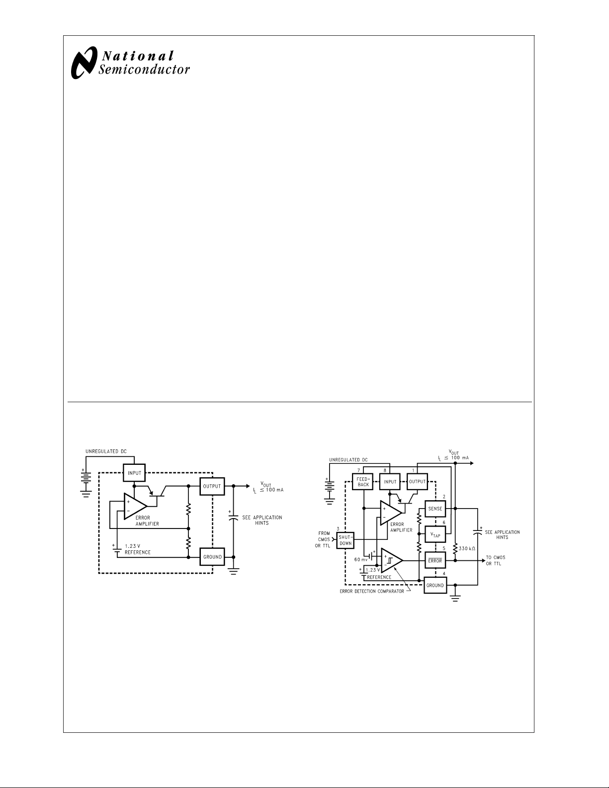
One such feature is an error flag output which warns of a low
output voltage, often due to falling batteries on the input. It
may be used for a power-on reset. A second feature is the
logic-compatible shutdown input which enables the regulator
to be switched on and off. Also, the part may be pin-strapped
for a 5V, 3V, or 3.3V output (depending on the version), or
programmed from 1.24V to 29V with an external pair of
resistors.
Careful design of the LP2950/LP2951 has minimized all
contributions to the error budget. This includes a tight initial
tolerance (.5% typ.), extremely good load and line regulation
(.05% typ.) and a very low output voltage temperature coefficient, making the part useful as a low-power voltage reference.
Features
n 5V, 3V, and 3.3V versions available
n High accuracy output voltage
n Guaranteed 100mA output current
n Extremely low quiescent current
n Low dropout voltage
n Extremely tight load and line regulation
n Very low temperature coefficient
n Use as Regulator or Reference
n Needs minimum capacitance for stability
n Current and Thermal Limiting
n Stable with low-ESR output capacitors
LP2951 versions only
n Error flag warns of output dropout
n Logic-controlled electronic shutdown
n Output programmable from 1.24 to 29V
LP2950/LP2951 Series of Adjustable Micropower Voltage Regulators
May 2003
Block Diagram and Typical Applications
LP2950 LP2951
00854625
00854601
© 2003 National Semiconductor Corporation DS008546 www.national.com
Page 2
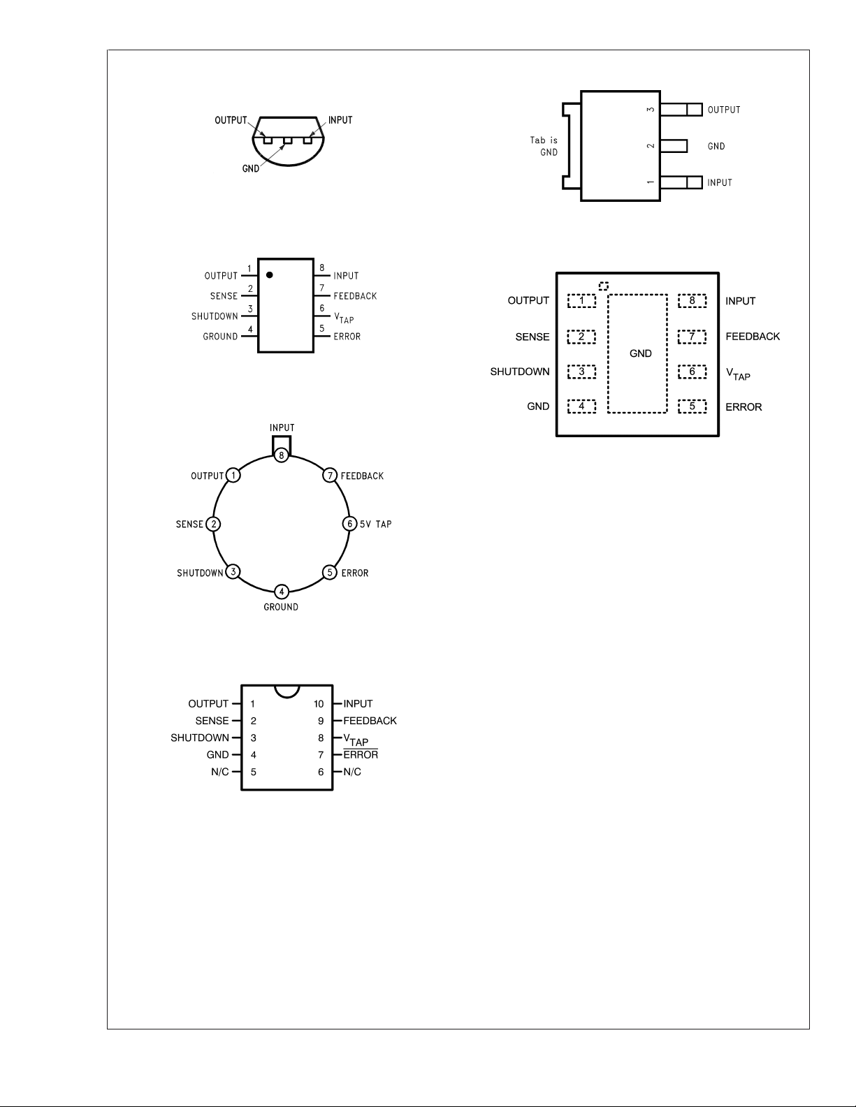
Connection Diagrams
TO-92 Plastic Package (Z)
LP2950/LP2951
TO-252 (D-Pak)
Bottom View
00854602
Dual-In-Line Packages (N, J)
Surface-Mount Package (M, MM)
00854626
Top View
Metal Can Package (H)
Front View
00854670
8-Lead LLP
00854671
Pin 4 is fused to center DAP
Top View
Top View
00854619
10-Lead Ceramic Surface-Mount Package (WG)
Top View
00854664
www.national.com 2
Page 3
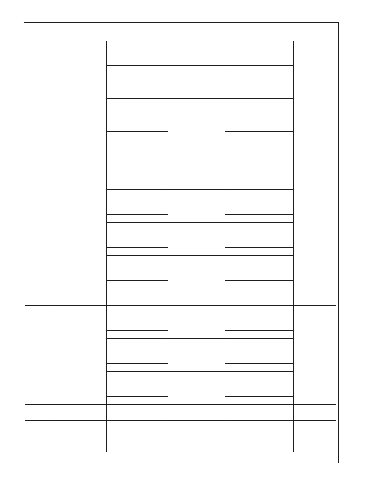
Ordering Information
LP2950/LP2951
Package Temperature
Range
<
<
−40
<
<
<
−40
<
<
−55<T
T
J
T
J
T
J
T
J
T
J
T
J
T
J
J
TO-92 (Z) −40
TO-252
(D-Pak)
N (N-08E) −40
M (M08A) −40
MM
(MUA08A)
J (J08A) −55
H (H08C) −55
WG
(WG10A)
Part Number Package Marking Transport Media NSC Drawing
<
125 LP2950ACZ-3.0 2950A CZ3.0 Bag Z03A
LP2950CZ-3.0 2950 CZ3.0 Bag
LP2950ACZ-3.3 2950A CZ3.3 Bag
LP2950CZ-3.3 2950 CZ3.3 Bag
LP2950ACZ-5.0 2950A CZ5.0 Bag
LP2950CZ-5.0 2950 CZ5.0 Bag
<
125 LP2950CDT-3.0 LP2950CDT-3.0 75 Units/Rail TD03B
LP2950CDTX-3.0 2.5k Units Tape and Reel
LP2950CDT-3.3 LP2950CDT-3.3 75 Units/Rail
LP2950CDTX-3.3 2.5k Units Tape and Reel
LP2950CDT-5.0 LP2950CDT-5.0 75 Units/Rail
LP2950CDTX-5.0 2.5k Units Tape and Reel
<
125 LP2951ACN-3.0 LP2951ACN-3.0 40 Units/Rail N08E
LP2951CN-3.0 LP2951CN-3.0 40 Units/Rail
LP2951ACN-3.3 LP2951ACN-3.3 40 Units/Rail
LP2951CN-3.3 LP2951CN-3.3 40 Units/Rail
LP2951ACN LP2951ACN 40 Units/Rail
LP2951CN LP2951CN 40 Units/Rail
<
125 LP2951ACM-3.0 2951ACM30DD 95 Units/Rail M08A
LP2951ACMX-3.0 2.5k Units Tape and Reel
LP2951CM-3.0 2951CM30DD 95 Units/Rail
LP2951CMX-3.0 2.5k Units Tape and Reel
LP2951ACM-3.3 2951ACM33DD 95 Units/Rail
LP2951ACMX-3.3 2.5k Units Tape and Reel
LP2951CM-3.3 2951CM33DD 95 Units/Rail
LP2951CMX-3.3 2.5k Units Tape and Reel
LP2951ACM 2951ACMDD 95 Units/Rail
LP2951ACMX 2.5k Units Tape and Reel
LP2951CM 2951CMDD 95 Units/Rail
LP2951CMX 2.5k Units Tape and Reel
<
125 LP2951ACMM-3.0 L0BA 1k Units Tape and Reel MUA08A
LP2951ACMMX-3.0 3.5k Units Tape and Reel
LP2951CMM-3.0 L0BB 1k Units Tape and Reel
LP2951CMMX-3.0 3.5k Units Tape and Reel
LP2951ACMM-3.3 L0CA 1k Units Tape and Reel
LP2951ACMMX-3.3 3.5k Units Tape and Reel
LP2951CMM-3.3 L0CB 1k Units Tape and Reel
LP2951CMMX-3.3 3.5k Units Tape and Reel
LP2951ACMM L0DA 1k Units Tape and Reel
LP2951ACMMX 3.5k Units Tape and Reel
LP2951CMM L0DB 1k Units Tape and Reel
LP2951CMMX 3.5k Units Tape and Reel
<
150 LP2951J/883 See MIL/AERO
Datasheet
<
150 LP2951H/883 See MIL/AERO
Datasheet
<
150 LP2951WG/883 See MIL/AERO
Datasheet
40 Units/Rail J08A
Tray H08C
Tray WG10A
www.national.com3
Page 4
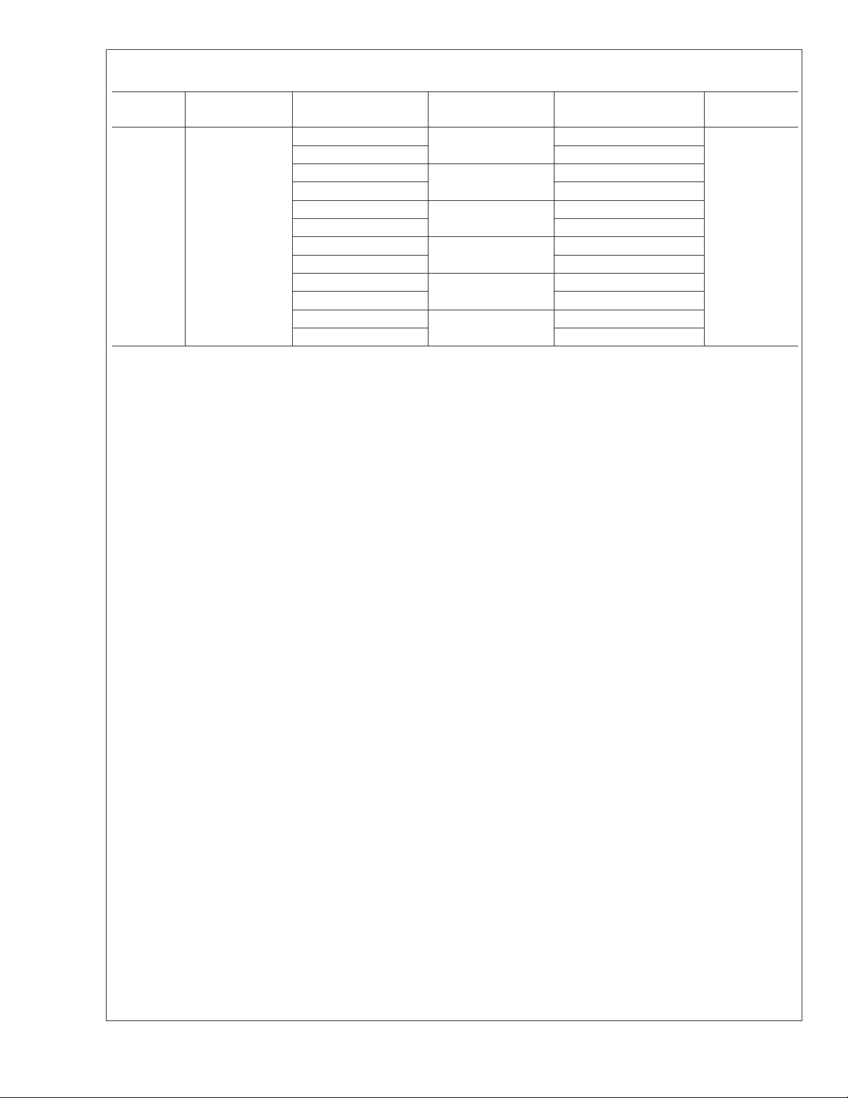
Ordering Information (Continued)
Package Temperature
8-lead LLP −40<T
LP2950/LP2951
Part Number Package Marking Transport Media NSC Drawing
Range
<
125 LP2951ACLD-3.0 L002A 1k Units Tape and Reel LDA08A
J
LP2951ACLDX-3.0 4.5k Units Tape and Reel
LP2951CLD-3.0 L002B 1k Units Tape and Reel
LP2951CLDX-3.0 4.5k Units Tape and Reel
LP2951ACLD-3.3 L003A 1k Units Tape and Reel
LP2951ACLDX-3.3 4.5k Units Tape and Reel
LP2951CLD-3.3 L003B 1k Units Tape and Reel
LP2951CLDX-3.3 4.5k Units Tape and Reel
LP2951ACLD-5.0 L027A 1k Units Tape and Reel
LP2951ACLDX-5.0 4.5k Units Tape and Reel
LP2951CLD-5.0 L027B 1k Units Tape and Reel
LP2951CLDX-5.0 4.5k Units Tape and Reel
www.national.com 4
Page 5
LP2950/LP2951
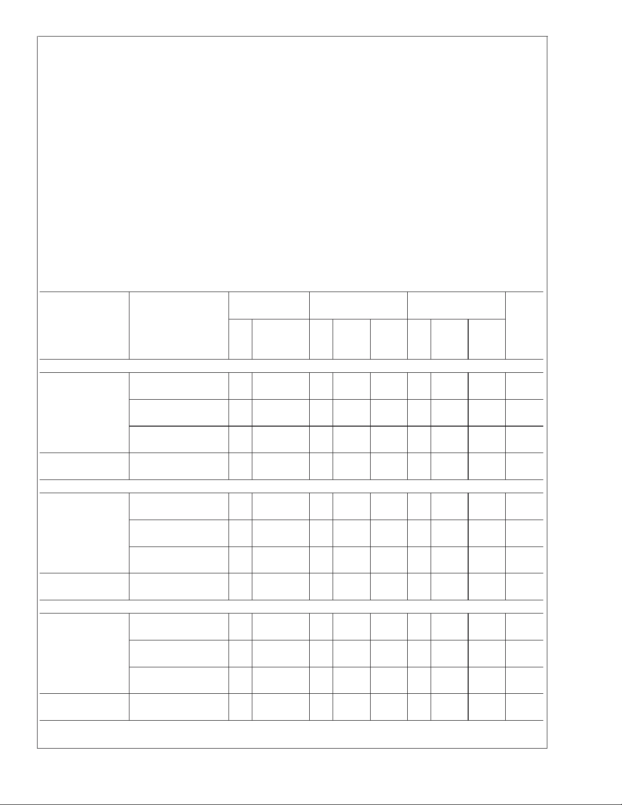
Absolute Maximum Ratings (Note 1)
If Military/Aerospace specified devices are required,
please contact the National Semiconductor Sales Office/
Distributors for availability and specifications.
Input Supply Voltage −0.3 to +30V
SHUTDOWN Input Voltage,
Error Comparator Output
Voltage, (Note 9)
FEEDBACK Input Voltage −1.5 to +30V
(Note 9) (Note 10)
Power Dissipation Internally Limited
Junction Temperature (T
) +150˚C
J
Ambient Storage Temperature −65˚ to +150˚C
Soldering Dwell Time, Temperature
Wave
Infrared
Vapor Phase
4 seconds, 260˚C
10 seconds, 240˚C
75 seconds, 219˚C
Electrical Characteristics (Note 2)
Parameter
3V Versions (Note 17)
Output Voltage T
Output Voltage 100µA ≤ I
3.3V Versions (Note 17)
Output Voltage T
Output Voltage 100µA ≤ I
5V Versions (Note 17)
Output Voltage T
Output Voltage 100µA ≤ I
Conditions
(Note 2)
= 25˚C 3.0 3.015 3.0 3.015 3.0 3.030 V max
J
−25˚C ≤ T
≤ 85˚C 3.0 3.0 3.030 3.0 3.045 V max
J
Typ Limit Typ Limit Limit Typ Limit Limit
Full Operating 3.0 3.036 3.0 3.036 3.0 3.060 V max
Temperature Range 2.964 2.964 2.940 V min
≤ 100mA 3.0 3.045 3.0 3.042 3.0 3.072 V max
L
T
≤ T
J
JMAX
= 25˚C 3.3 3.317 3.3 3.317 3.3 3.333 V max
J
−25˚C ≤ T
≤ 85˚C 3.3 3.3 3.333 3.3 3.350 V max
J
Full Operating 3.3 3.340 3.3 3.340 3.3 3.366 V max
Temperature Range 3.260 3.260 3.234 V min
≤ 100mA 3.3 3.350 3.3 3.346 3.3 3.379 V max
L
T
≤ T
J
JMAX
= 25˚C 5.0 5.025 5.0 5.025 5.0 5.05 V max
J
−25˚C ≤ T
≤ 85˚C 5.0 5.0 5.05 5.0 5.075 V max
J
Full Operating 5.0 5.06 5.0 5.06 5.0 5.1 V max
Temperature Range 4.94 4.94 4.9 V min
≤ 100mA 5.0 5.075 5.0 5.075 5.0 5.12 V max
L
T
≤ T
J
JMAX
ESD Rating
Human Body Model(Note 18) 2500V
Operating Ratings (Note 1)
Maximum Input Supply Voltage 30V
Junction Temperature Range
(T
) (Note 8)
J
LP2951 −55˚ to +150˚C
LP2950AC-XX, LP2950C-XX,
LP2951AC-XX, LP2951C-XX −40˚ to +125˚C
LP2951 LP2950AC-XX LP2950C-XX
LP2951AC-XX LP2951C-XX
Tested Tested Design Tested Design
(Notes 3, 16) (Note 3) (Note 4) (Note 3) (Note 4)
2.985 2.985 2.970 V min
2.970 2.955 V min
2.955 2.958 2.928 V min
3.284 3.284 3.267 V min
3.267 3.251 V min
3.251 3.254 3.221 V min
4.975 4.975 4.95 V min
4.95 4.925 V min
4.925 4.925 4.88 V min
Units
www.national.com5
Page 6
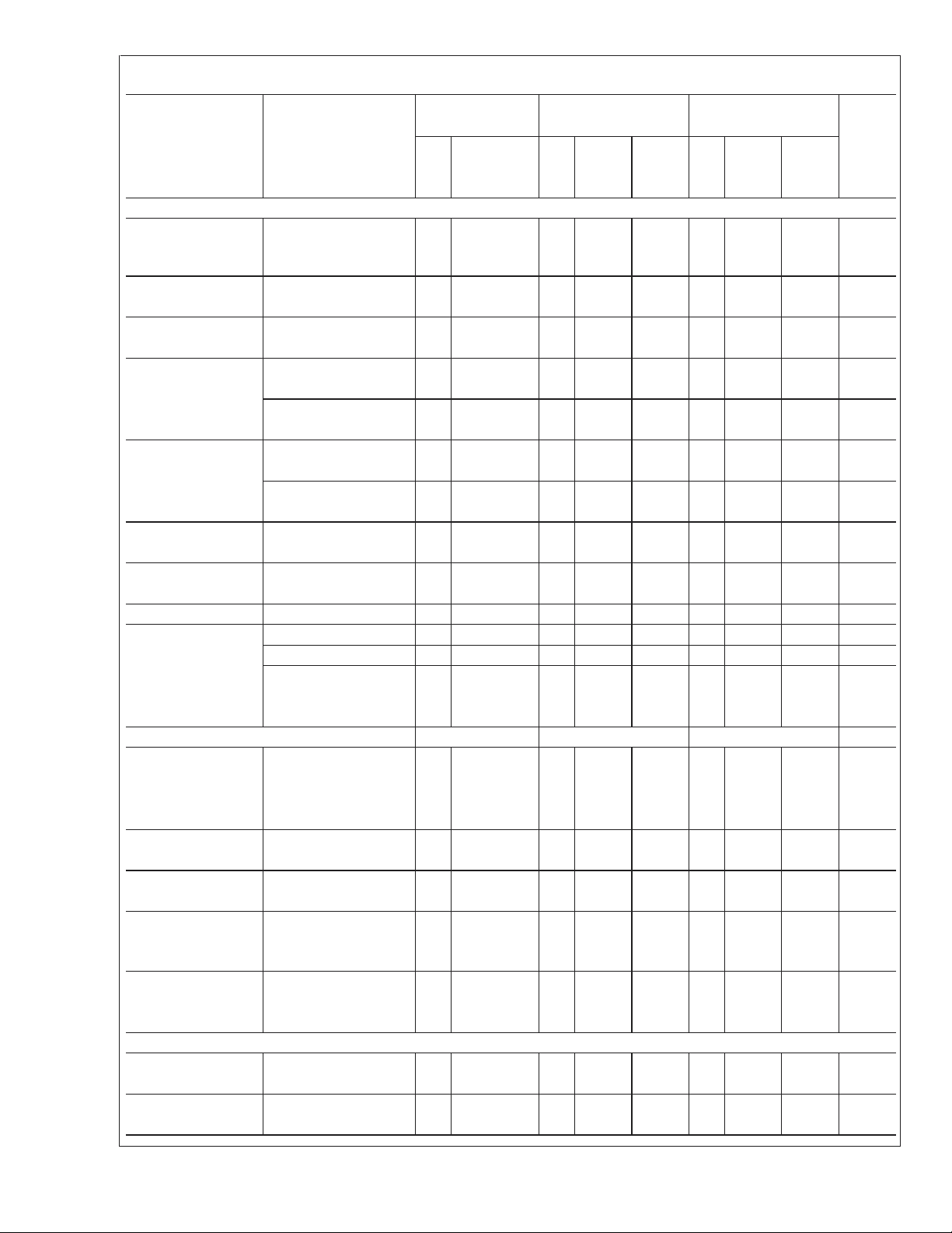
Electrical Characteristics (Note 2) (Continued)
LP2951 LP2950AC-XX LP2950C-XX
Parameter
LP2950/LP2951
Conditions
(Note 2)
Tested Tested Design Tested Design
Typ Limit Typ Limit Limit Typ Limit Limit
(Notes 3, 16) (Note 3) (Note 4) (Note 3) (Note 4)
All Voltage Options
Output Voltage
(Note 12) 20 120 20 100 50 150 ppm/˚C
Temperature
Coefficient
Line Regulation
(Note 14)
Load Regulation
(Note 14)
Dropout Voltage
(Note 5)
NOM + 1)V ≤ Vin≤
(V
O
30V (Note 15)
100µA ≤ I
I
= 100µA 80 80 80 mV max
L
I
= 100mA 450 450 450 mV max
L
≤ 100mA 0.04 0.1 0.04 0.1 0.1 0.2 % max
L
0.03 0.1 0.03 0.1 0.04 0.2 % max
0.5 0.2 0.4 % max
0.3 0.2 0.3 % max
50 150 50 150 50 150 mV max
380 600 380 600 380 600 mV max
Ground I
= 100µA 75 120 75 120 75 120 µA max
L
Current 140 140 140 µA max
I
= 100mA 8 12 8 12 8 12 mA max
L
14 14 14 mA max
Dropout V
Ground Current I
Current Limit V
=(VONOM − 0.5)V 110 170 110 170 110 170 µA max
in
= 100µA 200 200 200 µA max
L
= 0 160 200 160 200 160 200 mA max
out
220 220 220 mA max
Thermal Regulation (Note 13) 0.05 0.2 0.05 0.2 0.05 0.2 %/W max
Output Noise, C
10 Hz to 100 kHz C
= 1µF (5V Only) 430 430 430 µV rms
L
= 200µF 160 160 160 µV rms
L
C
= 3.3µF
L
(Bypass = 0.01µF 100 100 100 µV rms
Pins 7 to 1 (LP2951)
8-pin Versions Only LP2951 LP2951AC-XX LP2951C-XX
Reference 1.235 1.25 1.235 1.25 1.235 1.26 V max
Voltage 1.26 1.26 1.27 V max
1.22 1.22 1.21 V min
1.2 1.2 1.2 V min
Reference (Note 7) 1.27 1.27 1.285 V max
Voltage 1.19 1.19 1.185 V min
Feedback Pin 20 40 20 40 20 40 nA max
Bias Current 60 60 60 nA max
Reference Voltage (Note 12) 20 20 50 ppm/˚C
Temperature
Coefficient
Feedback Pin Bias 0.1 0.1 0.1 nA/˚C
Current Temperature
Coefficient
Error Comparator
Output Leakage V
= 30V 0.01 1 0.01 1 0.01 1 µA max
OH
Current 222µA max
Output Low V
Voltage I
=(VONOM − 0.5)V 150 250 150 250 150 250 mV max
in
= 400µA 400 400 400 mV max
OL
LP2951AC-XX LP2951C-XX
Units
www.national.com 6
Page 7
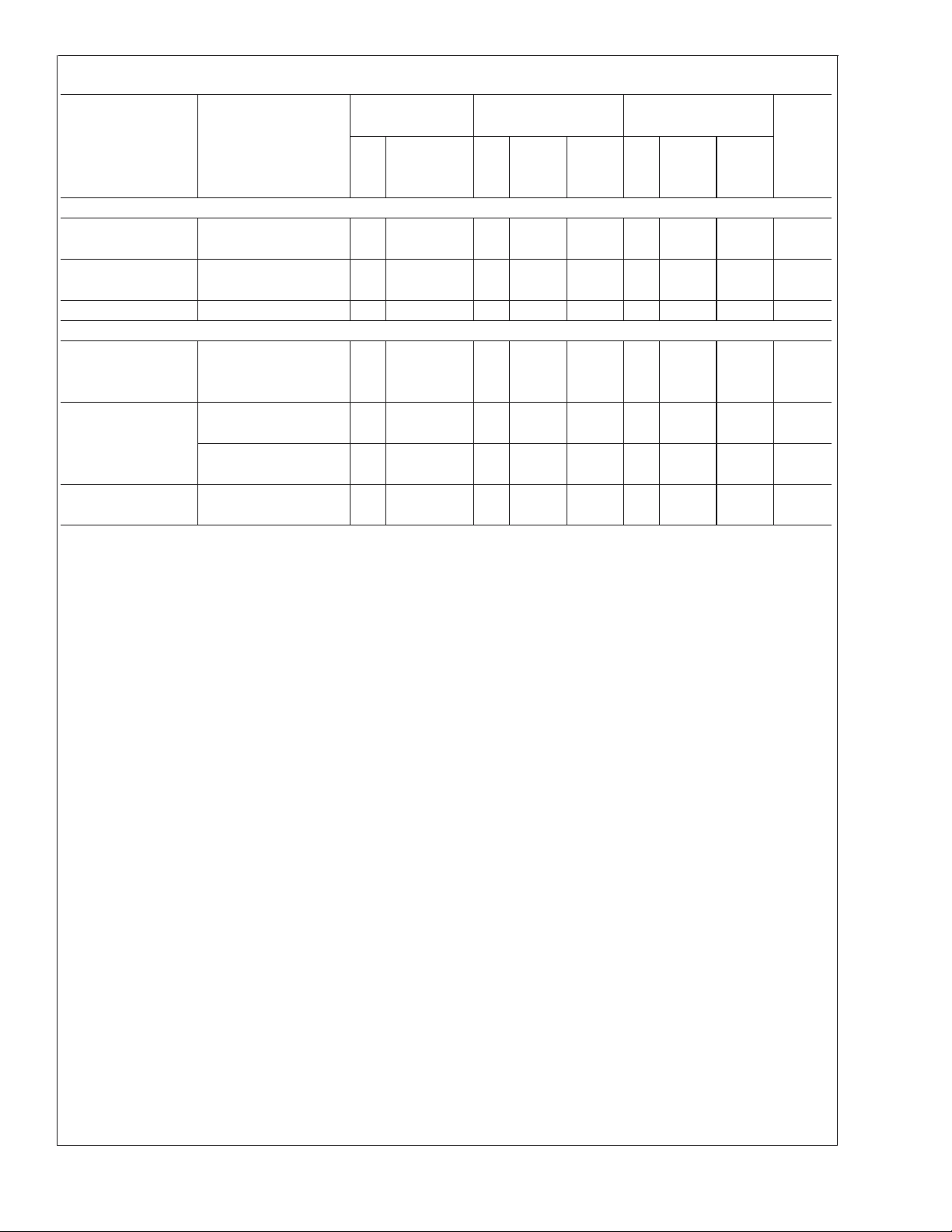
Electrical Characteristics (Note 2) (Continued)
LP2951 LP2950AC-XX LP2950C-XX
Parameter
Conditions
(Note 2)
Tested Tested Design Tested Design
Typ Limit Typ Limit Limit Typ Limit Limit
(Notes 3, 16) (Note 3) (Note 4) (Note 3) (Note 4)
Error Comparator
Upper Threshold (Note 6) 60 40 60 40 60 40 mV min
Voltage 25 25 25 mV min
Lower Threshold (Note 6) 75 95 75 95 75 95 mV max
Voltage 140 140 140 mV max
Hysteresis (Note 6) 15 15 15 mV
Shutdown Input
Input 1.3 1.3 1.3 V
Logic Low (Regulator ON) 0.6 0.7 0.7 V max
Voltage High (Regulator OFF) 2.0 2.0 2.0 V min
Shutdown Pin Input
Current
V
shutdown
V
shutdown
= 2.4V 30 50 30 50 30 50 µA max
100 100 100 µA max
= 30V 450 600 450 600 450 600 µA max
750 750 750 µA max
Regulator Output
Current in Shutdown
Note 1: Absolute Maximum Ratings are limits beyond which damage to the device may occur. Operating Ratings are conditions under which operation of the device
is guaranteed. Operating Ratings do not imply guaranteed performance limits. For guaranteed performance limits and associated test conditions, see the Electrical
Characteristics tables.
Note 2: Unless otherwise specified all limits guaranteed for V
Limits appearing in boldface type apply over the entire junction temperature range for operation. Limits appearing in normal type apply for T
conditions for the 8-pin versions are FEEDBACK tied to V
Note 3: Guaranteed and 100% production tested.
Note 4: Guaranteed but not 100% production tested. These limits are not used to calculate outgoing AQL levels.
Note 5: Dropout Voltage is defined as the input to output differential at which the output voltage drops 100 mV below its nominal value measured at 1V differential.
At very low values of programmed output voltage, the minimum input supply voltage of 2V (2.3V over temperature) must be taken into account.
Note 6: Comparator thresholds are expressed in terms of a voltage differential at the Feedback terminal below the nominal reference voltage measured at V
(V
NOM + 1)V. To express these thresholds in terms of output voltage change, multiply by the error amplifier gain = V
O
programmed output voltage of 5V, the Error output is guaranteed to go low when the output drops by 95mV x 5V/1.235V = 384 mV. Thresholds remain constant as
a percent of V
Note 7: V
Note 8: The junction-to-ambient thermal resistances are as follows: 180˚C/W and 160˚C/W for the TO-92 package with 0.40 inch and 0.25 inch leads to the printed
circuit board (PCB) respectively, 105˚C/W for the molded plastic DIP (N), 130˚C/W for the ceramic DIP (J), 160˚C/W for the molded plastic SOP (M), 200˚C/W for
the molded plastic MSOP (MM), and 160˚C/W for the metal can package (H). The above thermal resistances for the N, J, M, and MM packages apply when the
package is soldered directly to the PCB. Junction-to-case thermal resistance for the H package is 20˚C/W. Junction-to-case thermal resistance for the TO-252
package is 5.4˚C/W. The value of θ
thermal vias. For details of thermal resistance and power dissipation for the LLP package, refer to Application Note AN-1187.
Note 9: May exceed input supply voltage.
Note 10: When used in dual-supply systems where the output terminal sees loads returned to a negative supply, the output voltage should be diode-clamped to
ground.
Note 11: V
Note 12: Output or reference voltage temperature coefficient is defined as the worst case voltage change divided by the total temperature range.
Note 13: Thermal regulation is defined as the change in output voltage at a time T after a change in power dissipation is applied, excluding load or line regulation
effects. Specifications are for a 50mA load pulse at V
Note 14: Regulation is measured at constant junction temperature, using pulse testing with a low duty cycle. Changes in output voltage due to heating effects are
covered under the specification for thermal regulation.
Note 15: Line regulation for the LP2951 is tested at 150˚C for I
Performance Characteristics for line regulation versus temperature and load current.
Note 16: A Military RETS specification is available on request. At time of printing, the LP2951 RETS specification complied with the boldface limits in this column.
The LP2951H, WG, or J may also be procured as Standard Military Drawing Spec
Note 17: All LP2950 devices have the nominal output voltage coded as the last two digits of the part number. In the LP2951 products, the 3.0V and 3.3V versions
are designated by the last two digits, but the 5V version is denoted with no code at this location of the part number (refer to ordering information table).
Note 18: Human Body Model 1.5kΩ in series with 100pF.
out
≤ V
ref
shutdown
out
(Note 11) 3 10 3 10 3 10 µA max
20 20 20 µA max
=(V
IN
, OUTPUT tied to SENSE, and V
TAP
as V
is varied, with the dropout warning occurring at typically 5% below nominal, 7.5% guaranteed.
out
≤ (Vin− 1V), 2.3V ≤ Vin≤ 30V, 100µA ≤ IL≤ 100mA, TJ≤ T
for the LLP package is typically 51˚C/W but is dependent on the PCB trace area, trace material, and the number of layers and
JA
≥ 2V, Vin≤ 30V, V
= 0, Feedback pin tied to V
out
= 30V (1.25W pulse) for T = 10ms.
IN
= 1mA. For IL= 100µA and TJ= 125˚C, line regulation is guaranteed by design to 0.2%. See Typical
L
+ 1)V, IL= 100µA and CL= 1µF for 5V versions and 2.2µF for 3V and 3.3V versions.
ONOM
JMAX
.
TAP
#
LP2951AC-XX LP2951C-XX
SHUTDOWN
.
5962-3870501MGA, MXA, or MPA.
≤ 0.8V.
out/Vref
Units
= 25˚C. Additional
A=TJ
= (R1 + R2)/R2.For example, at a
in
=
LP2950/LP2951
www.national.com7
Page 8
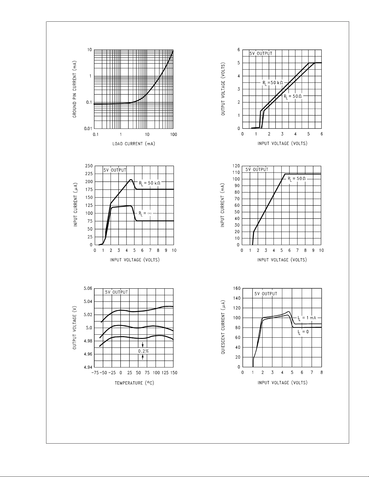
Typical Performance Characteristics
Quiescent Current Dropout Characteristics
LP2950/LP2951
00854627
Input Current Input Current
00854629
Output Voltage vs. Temperature of 3
Representative Units Quiescent Current
00854628
00854630
00854631
www.national.com 8
00854632
Page 9
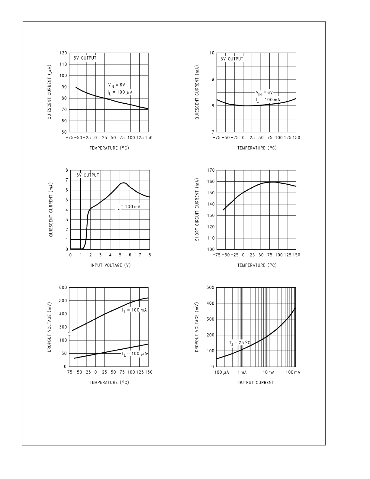
Typical Performance Characteristics (Continued)
Quiescent Current Quiescent Current
00854633 00854634
Quiescent Current Short Circuit Current
LP2950/LP2951
00854635
Dropout Voltage Dropout Voltage
00854637
00854636
00854638
www.national.com9
Page 10
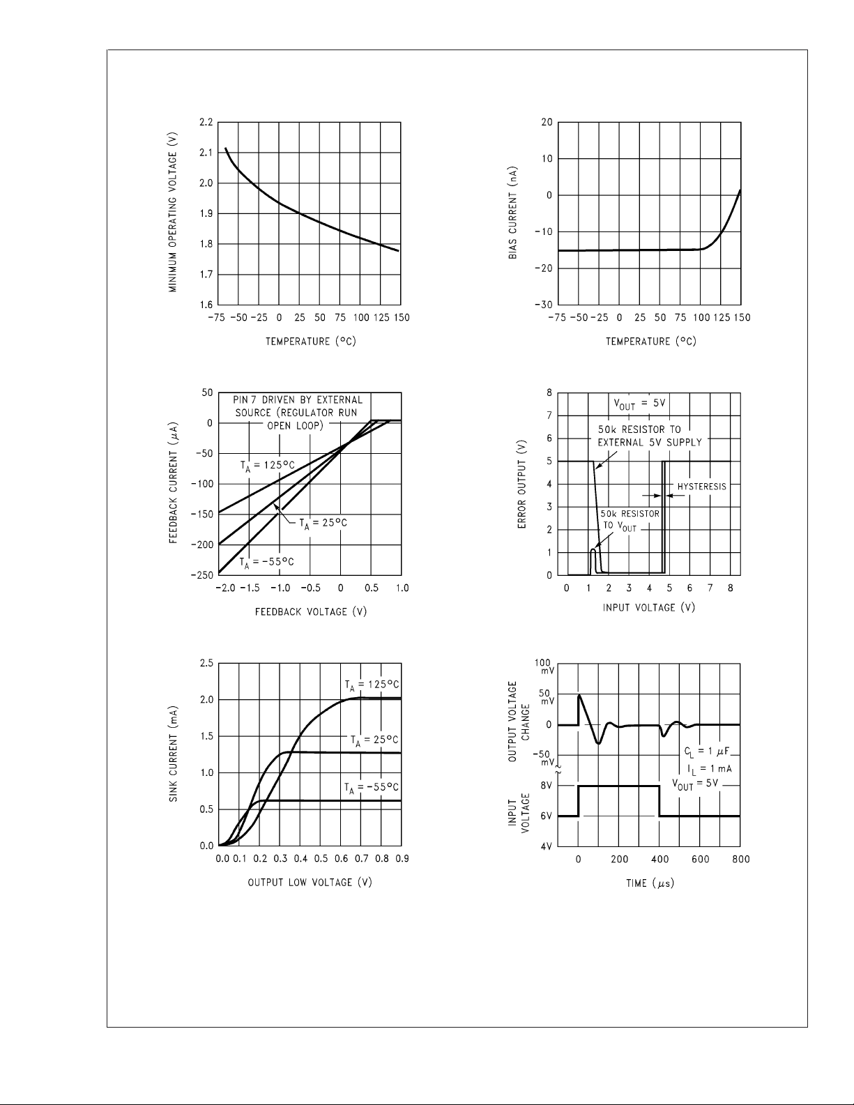
Typical Performance Characteristics (Continued)
LP2951 Minimum Operating Voltage LP2951 Feedback Bias Current
LP2950/LP2951
00854639 00854640
LP2951 Feedback Pin Current LP2951 Error Comparator Output
00854641
LP2951 Comparator Sink Current Line Transient Response
00854643
00854642
00854644
www.national.com 10
Page 11

Typical Performance Characteristics (Continued)
Load Transient Response Load Transient Response
00854645 00854646
LP2951 Enable Transient Output Impedance
LP2950/LP2951
00854647
Ripple Rejection Ripple Rejection
00854649 00854650
00854648
www.national.com11
Page 12
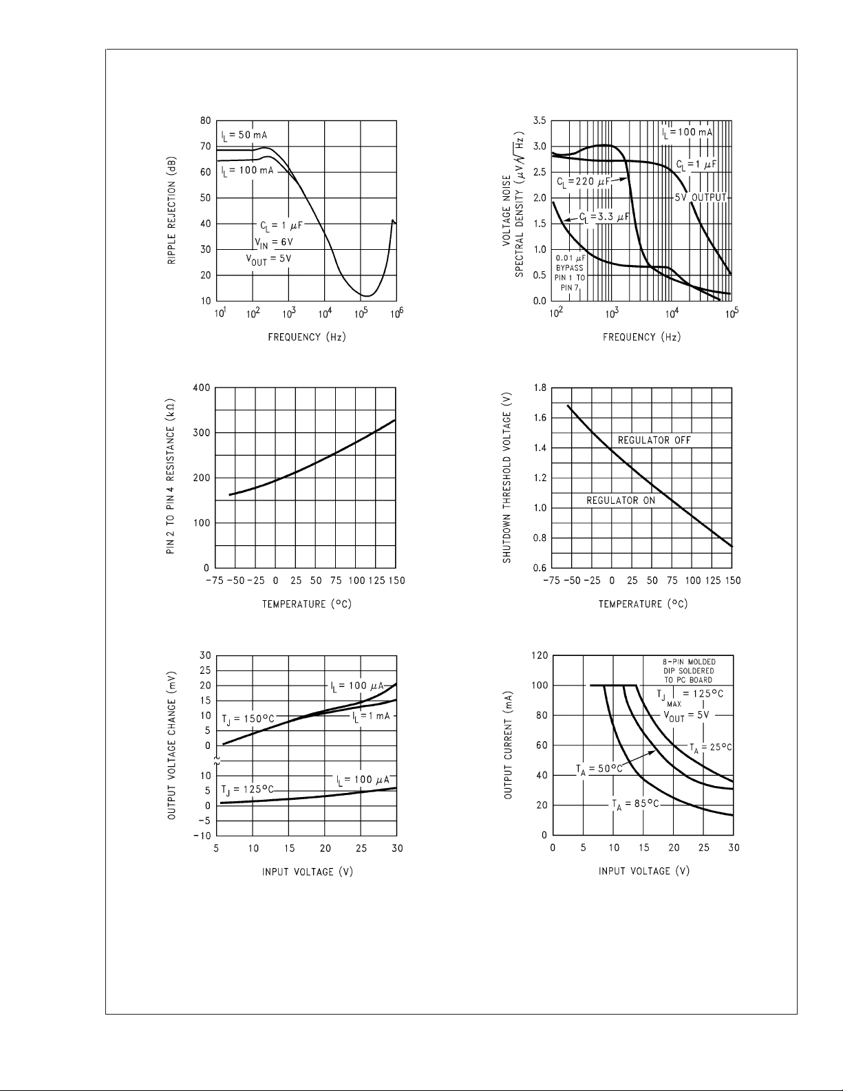
Typical Performance Characteristics (Continued)
Ripple Rejection LP2951 Output Noise
LP2950/LP2951
00854651 00854652
LP2951 Divider Resistance Shutdown Threshold Voltage
00854653
00854654
Line Regulation LP2951 Maximum Rated Output Current
00854655
00854656
www.national.com 12
Page 13
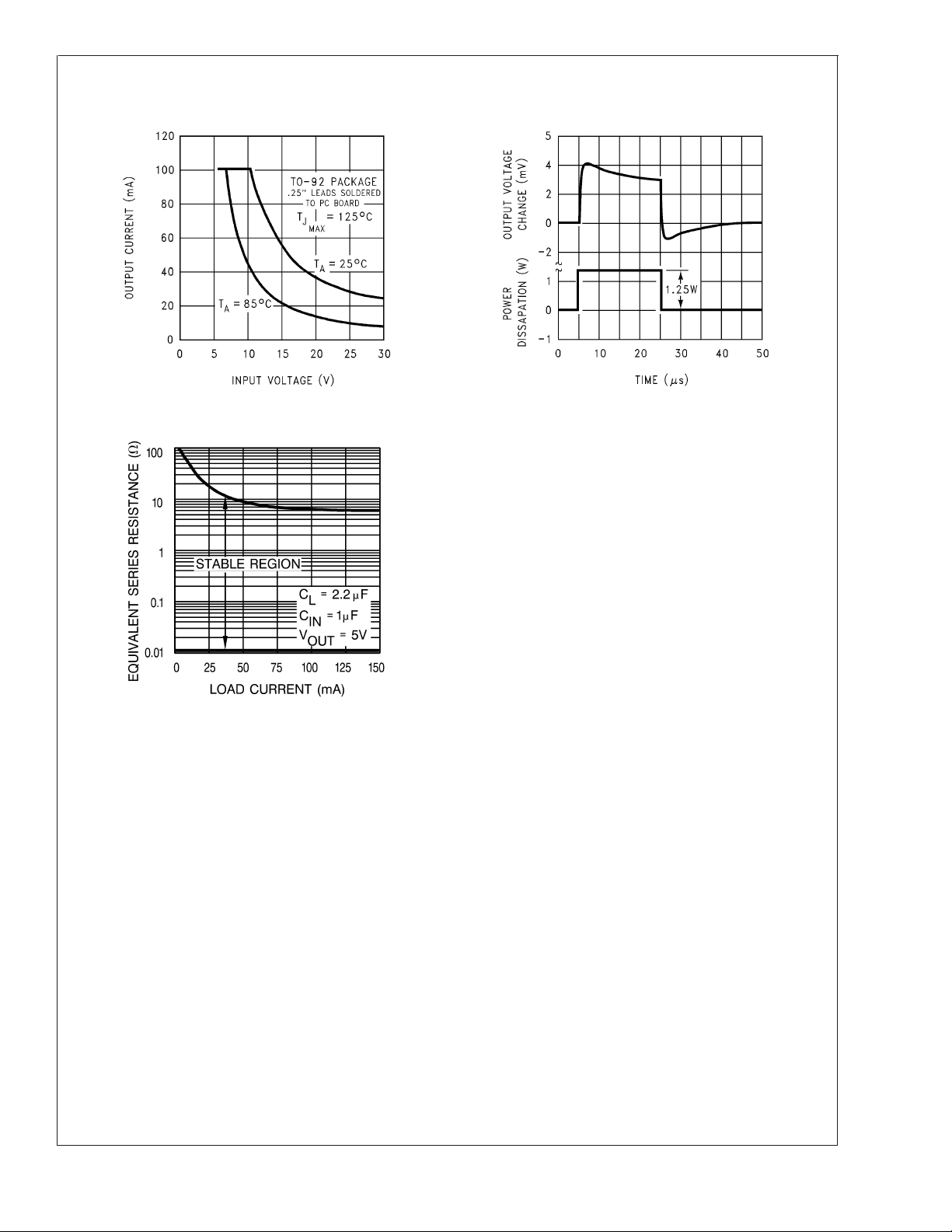
Typical Performance Characteristics (Continued)
LP2950 Maximum Rated Output Current Thermal Response
LP2950/LP2951
Output Capacitor ESR Range
00854657
00854663
00854658
www.national.com13
Page 14
Application Hints
EXTERNAL CAPACITORS
A 1.0µF (or greater) capacitor is required between the output
and ground for stability at output voltages of 5V or more. At
LP2950/LP2951
lower output voltages, more capacitance is required (2.2µF
or more is recommended for 3V and 3.3V versions). Without
this capacitor the part will oscillate. Most types of tantalum or
aluminum electrolytics work fine here; even film types work
but are not recommended for reasons of cost. Many aluminum electrolytics have electrolytes that freeze at about
−30˚C, so solid tantalums are recommended for operation
below −25˚C. The important parameters of the capacitor are
an ESR of about 5Ω or less and a resonant frequency above
500kHz. The value of this capacitor may be increased without limit.
Ceramic capacitors whose value is greater than 1000pF
should not be connected directly from the LP2951 output to
ground. Ceramic capacitors typically have ESR values in the
range of 5 to 10mΩ, a value below the lower limit for stable
operation (see curve Output Capacitor ESR Range).
The reason for the lower ESR limit is that the loop compensation of the part relies on the ESR of the output capacitor to
provide the zero that gives added phase lead. The ESR of
ceramic capacitors is so low that this phase lead does not
occur, significantly reducing phase margin. A ceramic output
capacitor can be used if a series resistance is added (recommended value of resistance about 0.1Ω to 2Ω).
At lower values of output current, less output capacitance is
required for stability. The capacitor can be reduced to 0.33µF
for currents below 10mA or 0.1µF for currents below 1mA.
Using the adjustable versions at voltages below 5V runs the
error amplifier at lower gains so that more output capacitance is needed. For the worst-case situation of a 100mA
load at 1.23V output (Output shorted to Feedback) a 3.3µF
(or greater) capacitor should be used.
Unlike many other regulators, the LP2950 will remain stable
and in regulation with no load in addition to the internal
voltage divider. This is especially important in CMOS RAM
keep-alive applications. When setting the output voltage of
the LP2951 versions with external resistors, a minimum load
of 1µA is recommended.
A 1µF tantalum, ceramic or aluminum electrolytic capacitor
should be placed from the LP2950/LP2951 input to ground if
there is more than 10 inches of wire between the input and
the AC filter capacitor or if a battery is used as the input.
Stray capacitance to the LP2951 Feedback terminal can
cause instability. This may especially be a problem when
using high value external resistors to set the output voltage.
Adding a 100pF capacitor between Output and Feedback
and increasing the output capacitor to at least 3.3µF will fix
this problem.
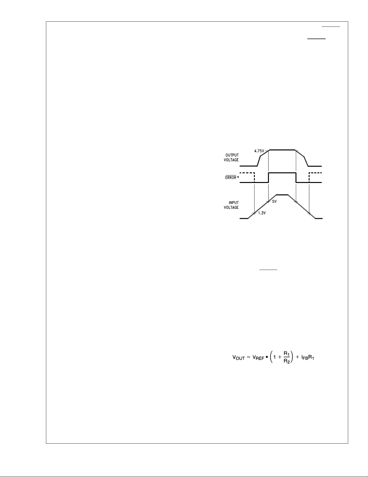
Figure 1 below gives a timing diagram depicting the ERROR
signal and the regulated output voltage as the LP2951 input
is ramped up and down. For 5V versions, the ERROR signal
becomes valid (low) at about 1.3V input. It goes high at
about 5V input (the input voltage at which V
OUT
= 4.75V).
Since the LP2951’s dropout voltage is load-dependent (see
curve in typical performance characteristics), the input voltage trip point (about 5V) will vary with the load current. The
output voltage trip point (approx. 4.75V) does not vary with
load.
The error comparator has an open-collector output which
requires an external pullup resistor. This resistor may be
returned to the output or some other supply voltage depending on system requirements. In determining a value for this
resistor, note that while the output is rated to sink 400µA, this
sink current adds to battery drain in a low battery condition.
Suggested values range from 100k to 1 MΩ. The resistor is
not required if this output is unused.
*
When VIN≤ 1.3V, the error flag pin becomes a high impedance, and the
error flag voltage rises to its pull-up voltage. Using V
voltage (see Figure 2), rather than an external 5V source, will keep the
error flag voltage under 1.2V (typ.) in this condition. The user may wish to
divide down the error flag voltage using equal-value resistors (10kΩ
suggested), to ensure a low-level logic signal during any fault condition,
while still allowing a valid high logic level during normal operation.
00854620
as the pull-up
OUT
FIGURE 1. ERROR Output Timing
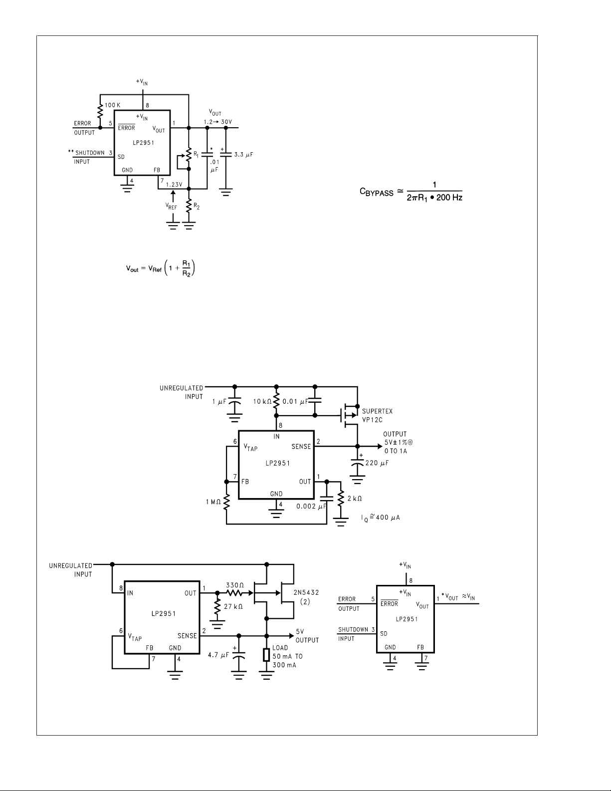
PROGRAMMING THE OUTPUT VOLTAGE (LP2951)
The LP2951 may be pin-strapped for the nominal fixed output voltage using its internal voltage divider by tying the
output and sense pins together, and also tying the feedback
and V
pins together. Alternatively, it may be programmed
TAP
for any output voltage between its 1.235V reference and its
30V maximum rating. As seen in Figure 2, an external pair of
resistors is required.
The complete equation for the output voltage is
ERROR DETECTION COMPARATOR OUTPUT
The comparator produces a logic low output whenever the
LP2951 output falls out of regulation by more than approximately 5%. This figure is the comparator’s built-in offset of
about 60mV divided by the 1.235 reference voltage. (Refer
to the block diagram in the front of the datasheet.) This trip
level remains “5% below normal” regardless of the programmed output voltage of the 2951. For example, the error
flag trip level is typically 4.75V for a 5V output or 11.4V for a
12V output. The out of regulation condition may be due
either to low input voltage, current limiting, or thermal limiting.
www.national.com 14
where V
is the nominal 1.235 reference voltage and IFBis
REF
the feedback pin bias current, nominally −20nA. The minimum recommended load current of 1µA forces an upper limit
of 1.2 MΩ on the value of R
no load (a condition often found in CMOS in standby). I
produce a 2% typical error in V
at room temperature by trimming R
choosing R
= 100k reduces this error to 0.17% while in-
2
, if the regulator must work with
2
which may be eliminated
OUT
. For better accuracy,
1
FB
will
creasing the resistor program current to 12µA. Since the
LP2951 typically draws 60µA at no load with Pin 2 opencircuited, this is a small price to pay.
Page 15
LP2950/LP2951
Application Hints (Continued)
*
See Application Hints
**
Drive with TTL-high to shut down. Ground or leave open if shutdown
feature is not to be used.
Note: Pins 2 and 6 are left open.
FIGURE 2. Adjustable Regulator
00854607
REDUCING OUTPUT NOISE
In reference applications it may be advantageous to reduce
the AC noise present at the output. One method is to reduce
the regulator bandwidth by increasing the size of the output
capacitor. This is the only way noise can be reduced on the
3 lead LP2950 but is relatively inefficient, as increasing the
capacitor from 1µF to 220µF only decreases the noise from
430µV to 160µV rms for a 100kHz bandwidth at 5V output.
Noise can be reduced fourfold by a bypass capacitor across
, since it reduces the high frequency gain from 4 to unity.
R
1
Pick
or about 0.01µF. When doing this, the output capacitor must
be increased to 3.3µF to maintain stability. These changes
reduce the output noise from 430µV to 100µV rms for a
100kHz bandwidth at 5V output. With the bypass capacitor
added, noise no longer scales with output voltage so that
improvements are more dramatic at higher output voltages.
Typical Applications
300mA Regulator with 0.75V Dropout Wide Input Voltage Range Current Limiter
1A Regulator with 1.2V Dropout
00854622
*
Minimum input-output voltage ranges from 40mV to 400mV, depending on
00854621
load current. Current limit is typically 160mA.
00854609
www.national.com15
Page 16
Typical Applications (Continued)
Low Drift Current Source 5 Volt Current Limiter
LP2950/LP2951
00854610
00854608
*
Minimum input-output voltage ranges from 40mV to 400mV, depending on
load current. Current limit is typically 160mA.
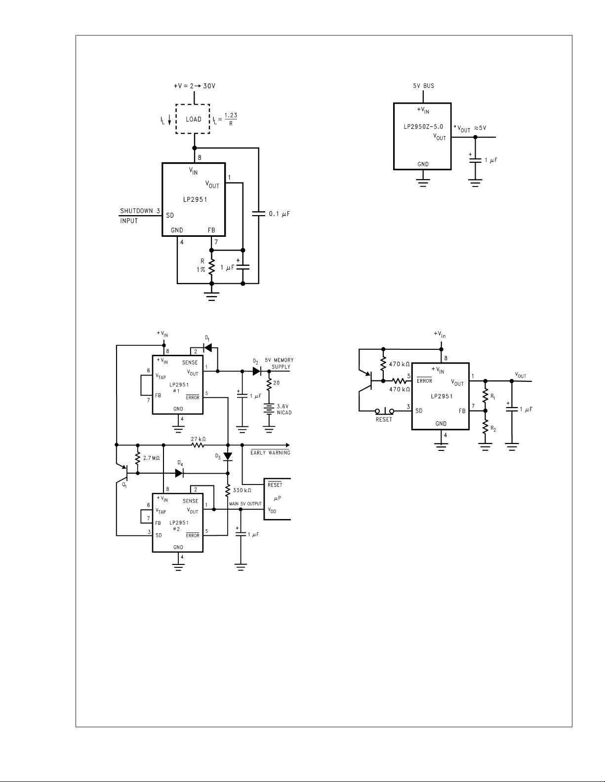
Regulator with Early Warning and Auxiliary Output Latch Off When Error Flag Occurs
00854612
j
Early warning flag on low input voltage
j
Main output latches off at lower input voltages
j
Battery backup on auxiliary output
j
Operation: Reg.#1’s V
error flag becomes active when V
error flag of Reg.
When V
warning signal rises, unlatching Reg.
#
again exceeds 5.7V Reg.#1 is back in regulation and the early
in
is programmed one diode drop above 5V. Its
out
2 becomes active and via Q1 latches the main output off.
≤ 5.7V. When Vindrops below 5.3V, the
in
#
2 via D3.
00854611
www.national.com 16
Page 17

Typical Applications (Continued)
2 Ampere Low Dropout Regulator
LP2950/LP2951
For 5V
, use internal resistors. Wire pin 6 to 7, & wire pin 2 to +V
out
5V Regulator with 2.5V Sleep Function
*
High input lowers V
out
to 2.5V
out
00854614
00854613
Bus.
Open Circuit Detector for 4→20mA Current Loop
00854615
www.national.com17
Page 18

Typical Applications (Continued)
LP2950/LP2951
Regulator with State-of-Charge Indicator
*
Optional Latch off when drop out occurs. Adjust R3 for C2 Switching when Vinis 6.0V.
**
Outputs go low when Vindrops below designated thresholds.
Low Battery Disconnect
<
For values shown, Regulator shuts down when V
*
Sets disconnect Voltage
**
Sets disconnect Hysteresis
5.5V and turns on again at 6.0V. Current drain in disconnected mode is ≈ 150µA.
in
00854616
00854617
www.national.com 18
Page 19

Typical Applications (Continued)
System Overtemperature Protection Circuit
LP2950/LP2951
LM34 for 125˚F Shutdown
LM35 for 125˚C Shutdown
00854618
www.national.com19
Page 20

LP2950/LP2951
00854623
Schematic Diagram
www.national.com 20
Page 21
Physical Dimensions inches (millimeters) unless otherwise noted
LP2950/LP2951
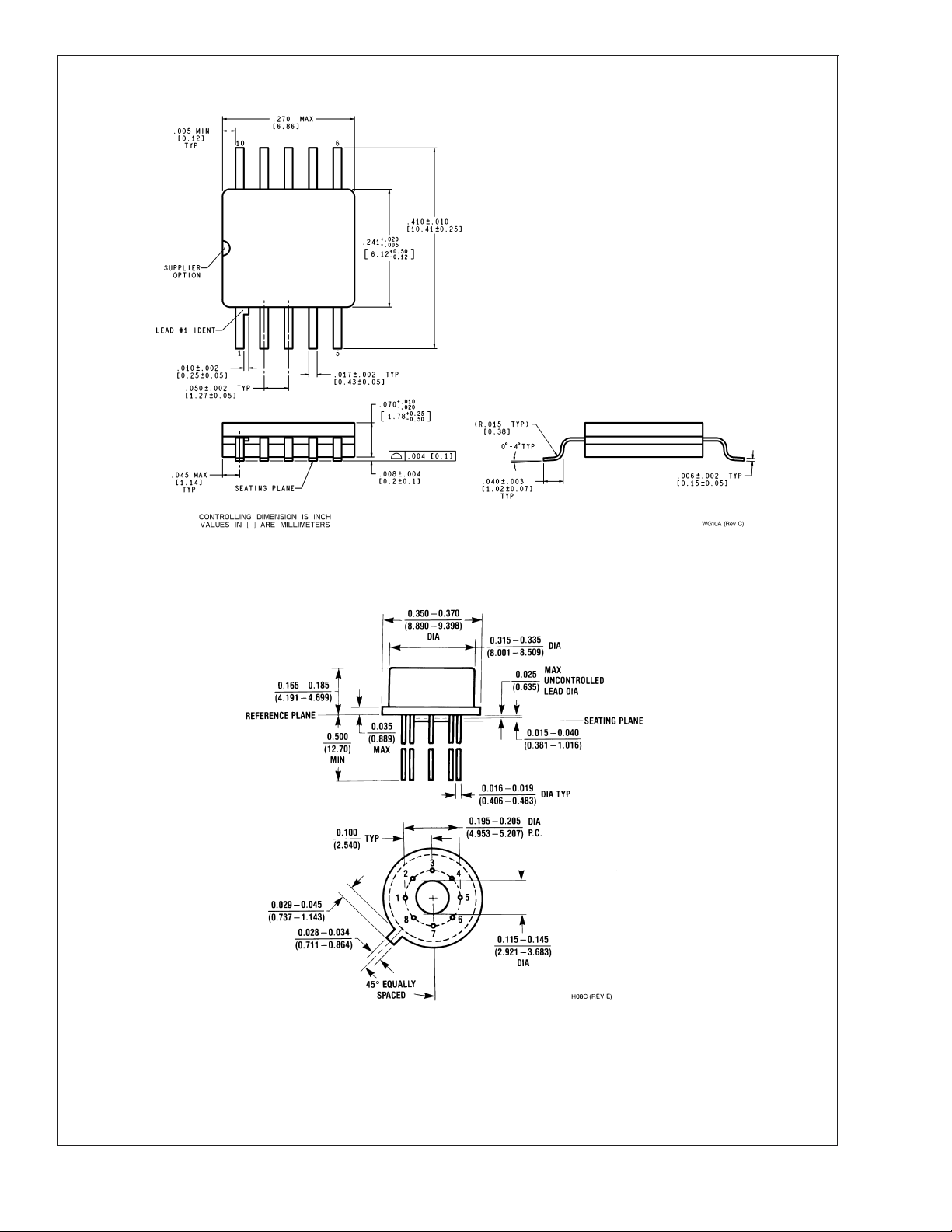
Order Number LP2951WG/883
NS Package Number WG10A
Metal Can Package (H)
NS Package Number H08C
www.national.com21
Page 22

Physical Dimensions inches (millimeters) unless otherwise noted (Continued)
LP2950/LP2951
Ceramic Dual-In-Line Package (J)
NS Package Number J08A
Surface Mount Package (M)
NS Package Number M08A
www.national.com 22
Page 23
Physical Dimensions inches (millimeters) unless otherwise noted (Continued)
LP2950/LP2951
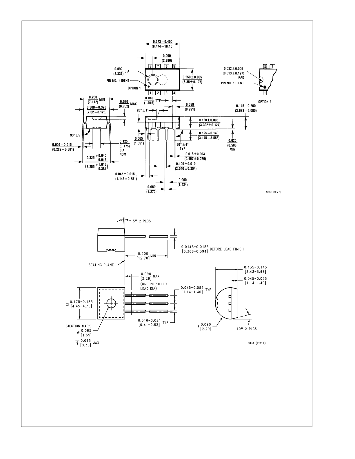
Molded Dual-In-Line Package (N)
NS Package Number N08E
Molded TO-92 Package (Z)
NS Package Number Z03A
www.national.com23
Page 24
Physical Dimensions inches (millimeters) unless otherwise noted (Continued)
LP2950/LP2951
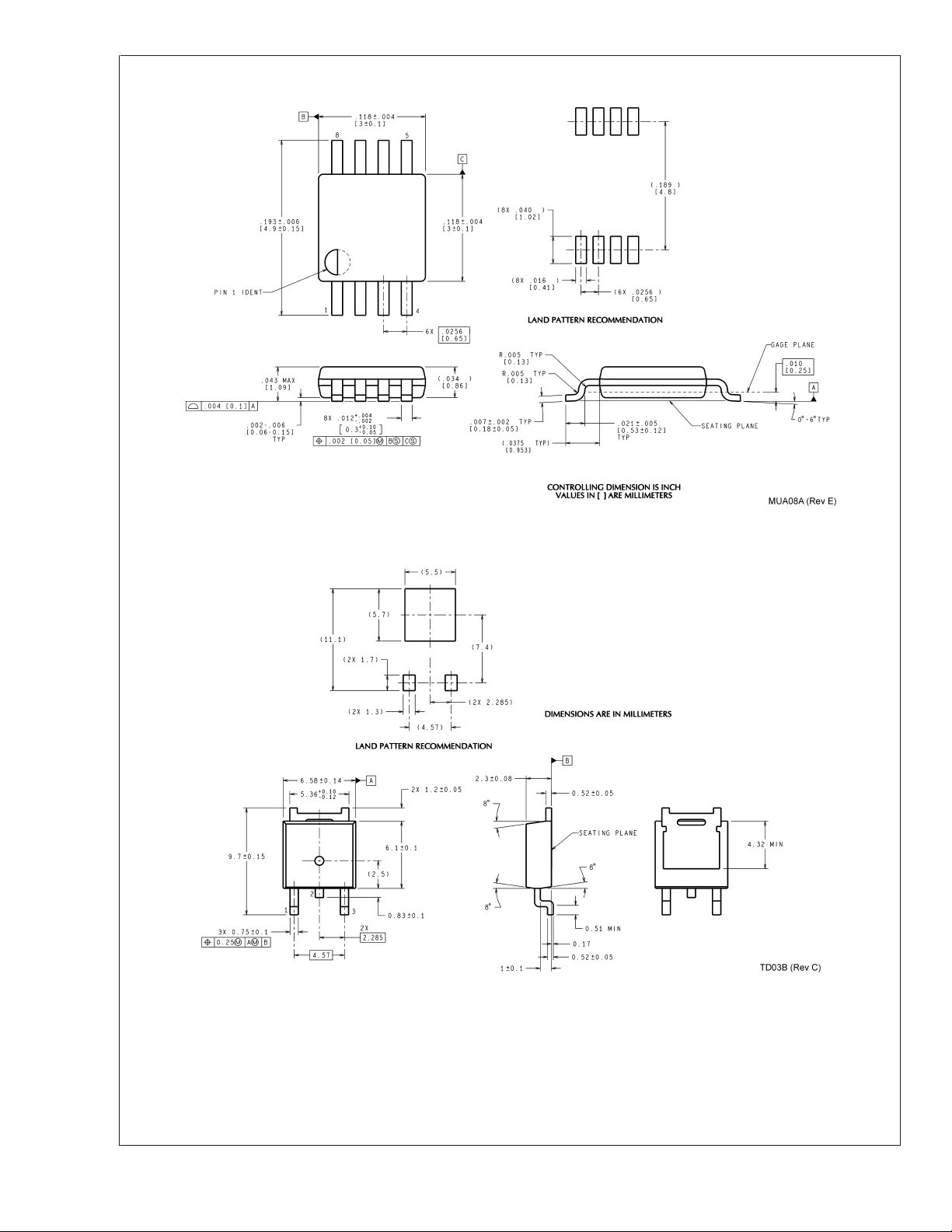
Surface Mount Package (MM)
NS Package Number MUA08A
D-Pak Package
NS Package Number TD03B
www.national.com 24
Page 25
Physical Dimensions inches (millimeters) unless otherwise noted (Continued)
LP2950/LP2951 Series of Adjustable Micropower Voltage Regulators
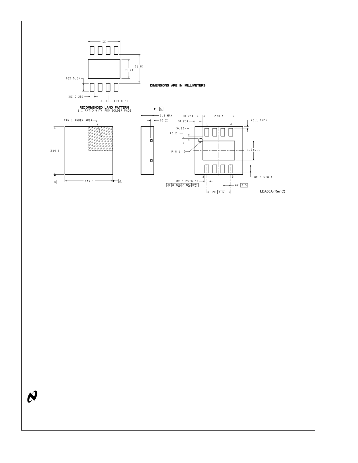
LLP Package
NS Package Number LDA08A
LIFE SUPPORT POLICY
NATIONAL’S PRODUCTS ARE NOT AUTHORIZED FOR USE AS CRITICAL COMPONENTS IN LIFE SUPPORT
DEVICES OR SYSTEMS WITHOUT THE EXPRESS WRITTEN APPROVAL OF THE PRESIDENT AND GENERAL
COUNSEL OF NATIONAL SEMICONDUCTOR CORPORATION. As used herein:
1. Life support devices or systems are devices or
systems which, (a) are intended for surgical implant
into the body, or (b) support or sustain life, and
whose failure to perform when properly used in
accordance with instructions for use provided in the
2. A critical component is any component of a life
support device or system whose failure to perform
can be reasonably expected to cause the failure of
the life support device or system, or to affect its
safety or effectiveness.
labeling, can be reasonably expected to result in a
significant injury to the user.
National Semiconductor
Americas Customer
Support Center
Email: [email protected]
Tel: 1-800-272-9959
www.national.com
National does not assume any responsibility for use of any circuitry described, no circuit patent licenses are implied and National reserves the right at any time without notice to change said circuitry and specifications.
National Semiconductor
Europe Customer Support Center
Fax: +49 (0) 180-530 85 86
Email: [email protected]
Deutsch Tel: +49 (0) 69 9508 6208
English Tel: +44 (0) 870 24 0 2171
Français Tel: +33 (0) 1 41 91 8790
National Semiconductor
Asia Pacific Customer
Support Center
Email: [email protected]
National Semiconductor
Japan Customer Support Center
Fax: 81-3-5639-7507
Email: [email protected]
Tel: 81-3-5639-7560
 Loading...