

Page 1
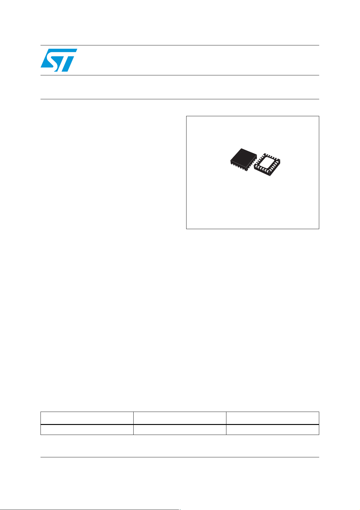
LNBH26S
Dual LNBS supply and control IC with step-up and I²C interface
Datasheet − preliminary data
Features
■ Complete interface between LNB and I²C bus
■ Built-in DC-DC converter for single 12 V supply
operation and high efficiency (typ. 93% @
0.5 A)
■ Selectable output current limit by external
resistor
■ Compliant with main satellite receiver output
voltage specification (8 programmable levels)
■ Accurate built-in 22 kHz tone generator suits
widely accepted standards
■ 22 kHz tone waveform integrity guaranteed
also at no load condition
■ Low-drop post regulator and high efficiency
step-up PWM with integrated power N-MOS
allowing low power losses
■ Overload and overtemperature internal
protection with I²C diagnostic bits
■ LNB short-circuit dynamic protection
■ +/- 4 kV ESD tolerant on output power pins
Applications
■ STB satellite receivers
■ TV satellite receivers
■ PC card satellite receivers
Description
Intended for analog and digital DUAL satellite
receivers/Sat-TV, Sat-PC cards, the LNBH26S is
a monolithic voltage regulator and interface IC,
assembled in QFN24 (4x4) specifically designed
to provide the 13 / 18 V power supply and the 22
kHz tone signalling to the LNB down-converter in
the antenna dishes or to the multi-switch box. In
this application field, it offers a complete solution
for dual tuner satellite receivers with an extremely
low component count and low power dissipation
together with simple design and I²C standard
interfacing.
QFN24 (4x4 mm)
Table 1. Device summary
Order code Package Packaging
LNBH26SPQR QFN24 (4x4) Tape and reel
March 2012 Doc ID 022995 Rev 1 1/29
This is preliminar y information on a new product now in development or undergoing evaluation. Details are subject to
change without notice.
www.st.com
29
Page 2

Contents LNBH26S
Contents
1 Block diagram . . . . . . . . . . . . . . . . . . . . . . . . . . . . . . . . . . . . . . . . . . . . . . 3
2 Application information (valid for each section A/B) . . . . . . . . . . . . . . . 4
2.1 DISEQC data encoding (DSQIN pin) . . . . . . . . . . . . . . . . . . . . . . . . . . . . . 4
2.2 Data encoding by external 22 kHz tone TTL signal . . . . . . . . . . . . . . . . . . 4
2.3 Data encoding by external DiSEqC envelope control
through the DSQIN pin . . . . . . . . . . . . . . . . . . . . . . . . . . . . . . . . . . . . . . . . 5
2.4 Output current limit selection . . . . . . . . . . . . . . . . . . . . . . . . . . . . . . . . . . . 5
2.5 Output voltage selection . . . . . . . . . . . . . . . . . . . . . . . . . . . . . . . . . . . . . . . 6
2.6 Diagnostic and protection functions . . . . . . . . . . . . . . . . . . . . . . . . . . . . . . 6
2.7 Surge protection and TVS diodes . . . . . . . . . . . . . . . . . . . . . . . . . . . . . . . 6
2.8 Power-on I²C interface reset and undervoltage lockout . . . . . . . . . . . . . . . 7
2.9 PNG: input voltage minimum detection . . . . . . . . . . . . . . . . . . . . . . . . . . . 7
2.10 OLF: overcurrent and short-circuit protection and diagnostic . . . . . . . . . . . 7
2.11 OTF: thermal protection and diagnostic . . . . . . . . . . . . . . . . . . . . . . . . . . . 8
3 Pin configuration . . . . . . . . . . . . . . . . . . . . . . . . . . . . . . . . . . . . . . . . . . . . 9
4 Maximum ratings . . . . . . . . . . . . . . . . . . . . . . . . . . . . . . . . . . . . . . . . . . . 11
5 Typical application circuits . . . . . . . . . . . . . . . . . . . . . . . . . . . . . . . . . . 12
6 I²C bus interface . . . . . . . . . . . . . . . . . . . . . . . . . . . . . . . . . . . . . . . . . . . 13
6.1 Data validity . . . . . . . . . . . . . . . . . . . . . . . . . . . . . . . . . . . . . . . . . . . . . . . 13
6.2 START and STOP condition . . . . . . . . . . . . . . . . . . . . . . . . . . . . . . . . . . . 13
6.3 Byte format . . . . . . . . . . . . . . . . . . . . . . . . . . . . . . . . . . . . . . . . . . . . . . . . 13
6.4 Acknowledge . . . . . . . . . . . . . . . . . . . . . . . . . . . . . . . . . . . . . . . . . . . . . . 13
6.5 Transmission without acknowledge . . . . . . . . . . . . . . . . . . . . . . . . . . . . . 13
7 I²C interface protocol . . . . . . . . . . . . . . . . . . . . . . . . . . . . . . . . . . . . . . . 15
7.1 Write mode transmission . . . . . . . . . . . . . . . . . . . . . . . . . . . . . . . . . . . . . 15
7.2 Read mode transmission . . . . . . . . . . . . . . . . . . . . . . . . . . . . . . . . . . . . . 16
7.3 Data registers . . . . . . . . . . . . . . . . . . . . . . . . . . . . . . . . . . . . . . . . . . . . . . 17
2/29 Doc ID 022995 Rev 1
Page 3

LNBH26S Contents
7.4 Status registers . . . . . . . . . . . . . . . . . . . . . . . . . . . . . . . . . . . . . . . . . . . . 19
8 Electrical characteristics . . . . . . . . . . . . . . . . . . . . . . . . . . . . . . . . . . . . 21
8.1 Output voltage selection . . . . . . . . . . . . . . . . . . . . . . . . . . . . . . . . . . . . . . 22
9 Package mechanical data . . . . . . . . . . . . . . . . . . . . . . . . . . . . . . . . . . . . 24
10 Revision history . . . . . . . . . . . . . . . . . . . . . . . . . . . . . . . . . . . . . . . . . . . 28
Doc ID 022995 Rev 1 3/29
Page 4
Block diagram LNBH26S
V
1 Block diagram
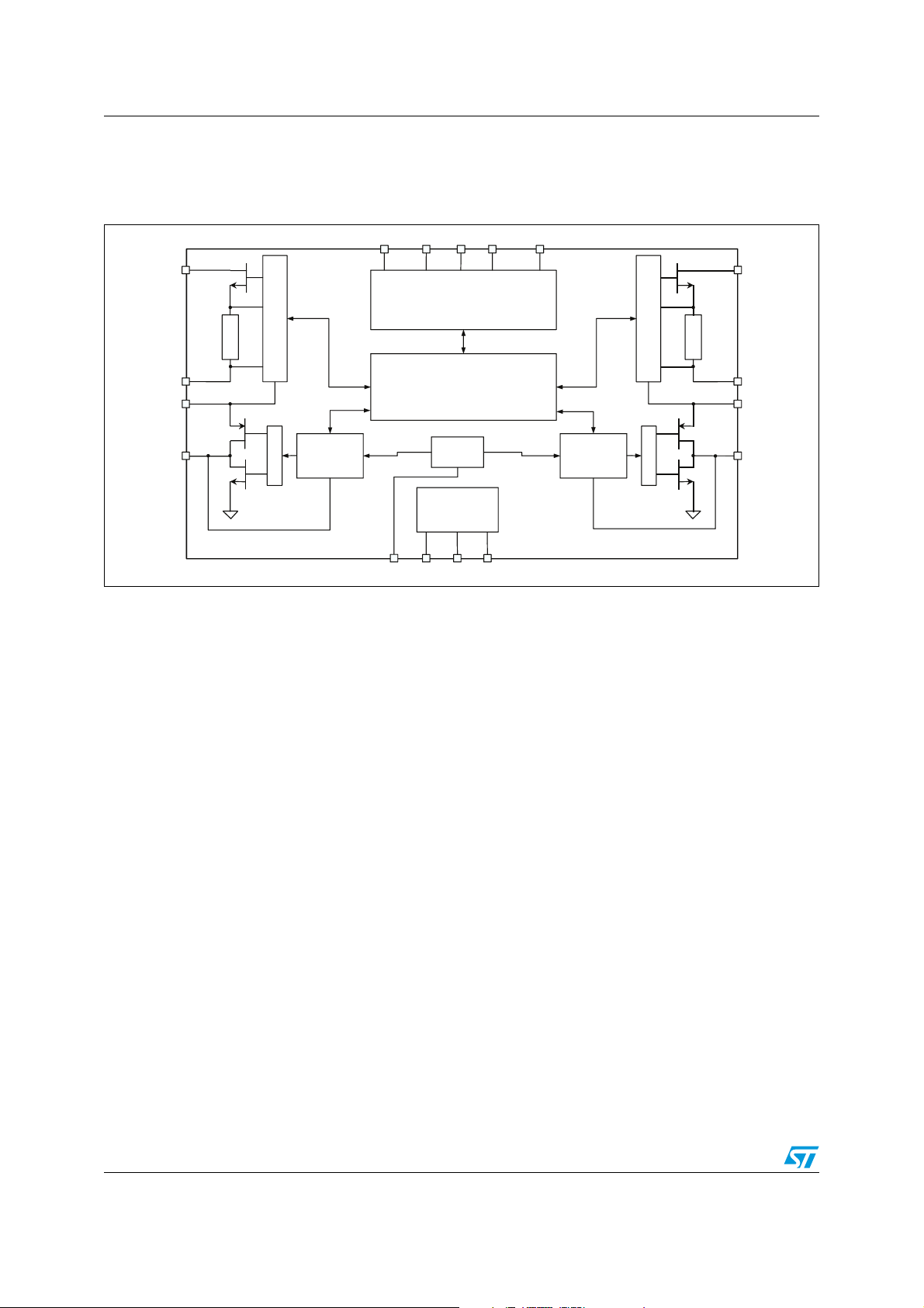
Figure 1. Block diagram
DSQIN-B
DSQIN-A
ADDR
SDASCL
LX-A
PGND
VUP-A
OUT-A
Isense
PWM CTRL
Gate ctrl
Linear
Regulator
ISEL
I²C Digital core
DAC
Drop control
Tone ctrl
Diagnostics
Protections
Current
Limit
selection
Voltage
reference
GND
BYP
VCC
Linear
Regulator
PWM CTRL
Gate ctrl
LX-B
Isense
PGND
VUP-B
VOUT-B
AM10482v 1
4/29 Doc ID 022995 Rev 1
Page 5

LNBH26S Application information (valid for each section A/B)
2 Application information (valid for each section A/B)
This IC has a built-in DC-DC step-up converter that, from a single source (8 V to 16 V),
generates the voltages (V
/ 18 V LNB output voltages plus the 22 kHz DiSEqC tone) to work with a minimum
dissipated power of 0.5 W typ. @ 500 mA load (the LDO drop voltage is internally kept at
V
- V
UP
disables the whole circuit when the supplied V
typically). The step-up converter soft-start function reduces the inrush current during
startup. The SS time is internally fixed at 4 ms typ. to switch from 0 to 13 V and 6 ms typ. to
switch from 0 to 18 V.
= 1 V typ.). The IC is also provided with an undervoltage lockout circuit that
OUT
2.1 DISEQC data encoding (DSQIN pin)
The internal 22 kHz tone generator is factory trimmed in accordance with the DiSEqC
standards, and can be activated in 3 different ways:
1) by an external 22 kHz source DiSEqC data connected to the DSQIN logic pin (TTL
compatible). In this case the I²C tone control bits must be set: EXTM=TEN=1.
2) by an external DiSEqC data envelope source connected to the DSQIN logic pin. In this
case the I²C tone control bits must be set: EXTM=0 and TEN=1.
) that let the integrated LDO post-regulator (generating the 13 V
UP
drops below a fixed threshold (4.7 V
CC
3) through the TEN I²C bit if the 22 kHz presence is requested in continuous mode. In this
case the DSQIN TTL pin must be pulled high and the EXTM bit set to “0”.
2.2 Data encoding by external 22 kHz tone TTL signal
In order to improve design flexibility, an external tone signal can be input to the DSQIN pin
by setting the EXTM bit to “1”.
The DSQIN is a logic input pin which activates the 22 kHz tone to the V
LNBH26S integrated tone generator.
The output tone waveforms are internally controlled by the LNBH26S tone generator in
terms of rise/fall time and tone amplitude, while, the external 22 kHz signal on the DSQIN
pin is used to define the frequency and the duty cycle of the output tone. A TTL compatible
22 kHz signal is required for the proper control of the DSQIN pin function. Before sending
the TTL signal on the DSQIN pin, the EXTM and TEN bits must be previously set to “1”. As
soon as the DSQIN internal circuit detects the 22 kHz TTL external signal code, the
LNBH26S activates the 22 kHz tone on the V
signal activation, and it stops with about 60 µs delay after the 22 kHz TTL signal on DSQIN
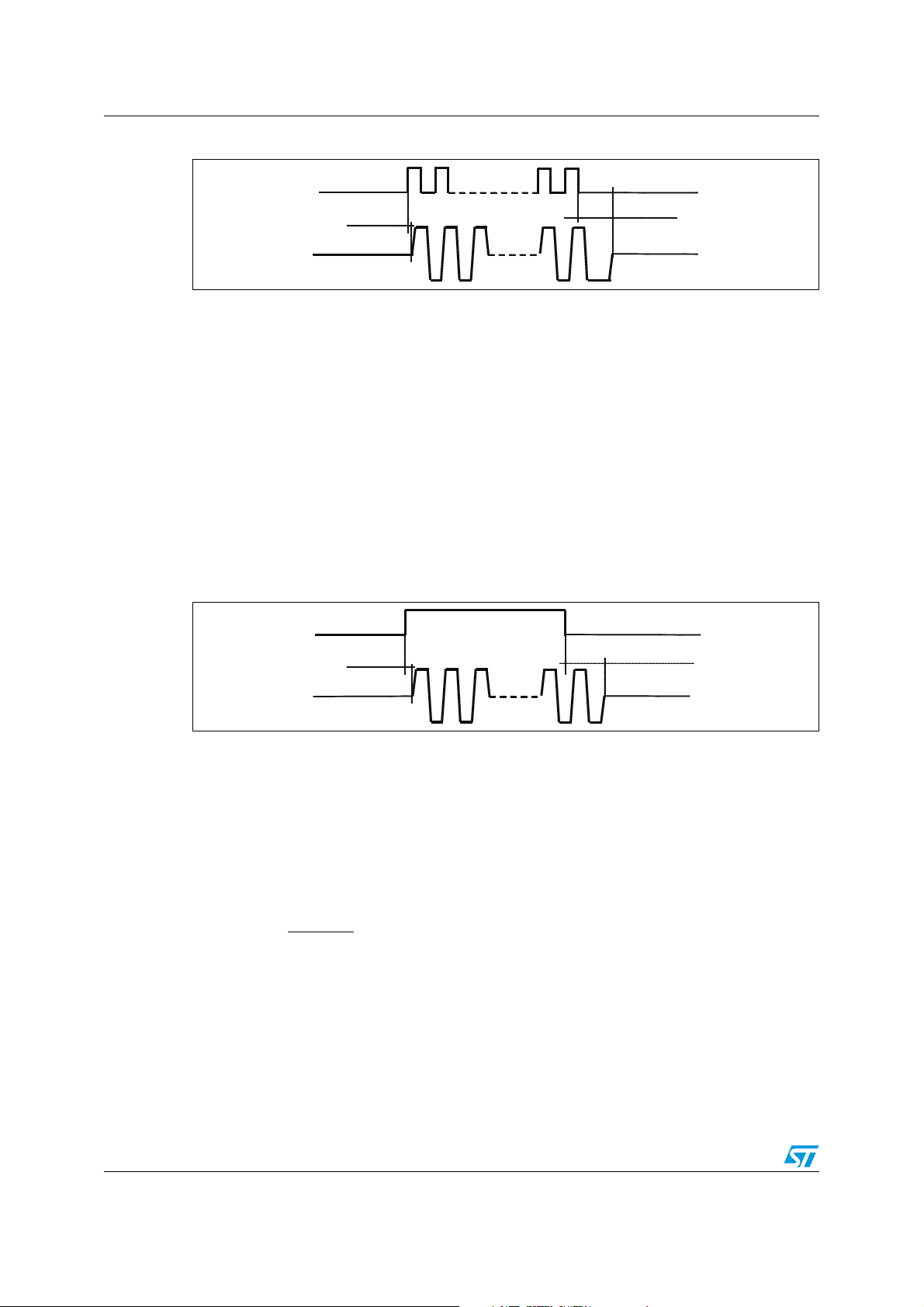
has expired. Refer to
Figure 2
.
output with about 1 µs delay from TTL
OUT
OUT
pin, by using the
Doc ID 022995 Rev 1 5/29
Page 6
Application information (valid for each section A/B) LNBH26S
Figure 2. Tone enable and disable timing (using external waveform)
DSQIN
Tone
~ 1 µs
Output
~ 60 µs
AM10426v1
2.3 Data encoding by external DiSEqC envelope control through the DSQIN pin
If an external DiSEqC envelope source is available, it is possible to use the internal 22 kHz
generator activated during the tone transmission by connecting the DiSEqC envelope
source to the DSQIN pin. In this case the I²C tone control bits must be set: EXTM=0 and
TEN=1. In this way, the internal 22 kHz signal is superimposed to the V
generate the LNB output 22 kHz tone. During the period in which the DSQIN is kept high the
internal control circuit activates the 22 kHz tone output.
The 22 kHz tone on the V
pin is activated with about 6 µs delay from the DSQIN TTL
OUT
signal rising edge, and it stops with a delay time in the range from 15 µs to 60 µs after the 22
kHz TTL signal on DSQIN has expired (refer to
Figure 3
).
Figure 3. Tone enable and disable timing (using envelope signal)
DSQIN
Tone
~ 6 µs
Output
15 µs ~ 60 µs
DC voltage to
OUT
2.4 Output current limit selection
The linear regulator current limit threshold can be set by an external resistor connected to
the ISEL pin. The resistor value defines the output current limit by the equation:
Equation 1
16578
=
MAX
with ISET=0,
where RSEL is the resistor connected between ISEL and GND expressed in kΩ and I
(typ.) is the typical current limit threshold expressed in mA. I
each channel. However, it is recommended to not exceed for a long period a total amount of
current of 1 A from both sections (I
overtemperature protection from triggering and to thoroughly validate the PCB layout
thermal management in real application environment conditions.
6/29 Doc ID 022995 Rev 1
.)typ(I
RSEL
206.1
+ I
OUT_A
OUT_B
AM10427v1
can be set up to 750 mA for
MAX
< 1 A) in order to avoid the
MAX
Page 7
LNBH26S Application information (valid for each section A/B)
2.5 Output voltage selection
Each linear regulator channel output voltage level can be easily programmed in order to
accomplish application specific requirements, using 4 + 4 bits of an internal DATA1 register
(see
Section 7.3: Data registers
register, write mode)
I²C bus.
for exact programmable values). Register writing is accessible via the
and
Table 13: Output voltage selection table (Data1
2.6 Diagnostic and protection functions
The LNBH26S has 4 diagnostic internal functions provided via the I²C bus, by reading 4 bits
on the STATUS1 register (in read mode). All the diagnostic bits are, in normal operation (that
is, no failure detected), set to LOW. One diagnostic bit is dedicated to the overtemperature
(OTF), and two bits (one per section) are dedicated to overcurrent (OLF-A, OLF-B). One bit
is dedicated to the input voltage power not good function (PNG). Once the OTF bit (or OLFA, OLF-B or PNG) has been activated (set to “1”), it is latched to “1” until the relevant cause
is removed and a new register reading operation is done.
2.7 Surge protection and TVS diodes
Each LNBH26S device section is directly connected to the antenna cable in a set-top box.
Atmospheric phenomenon can cause high voltage discharges on the antenna cable causing
damage to the attached devices. Surge pulses occur due to direct or indirect lightning
strikes to an external (outdoor) circuit. This leads to currents or electromagnetic fields
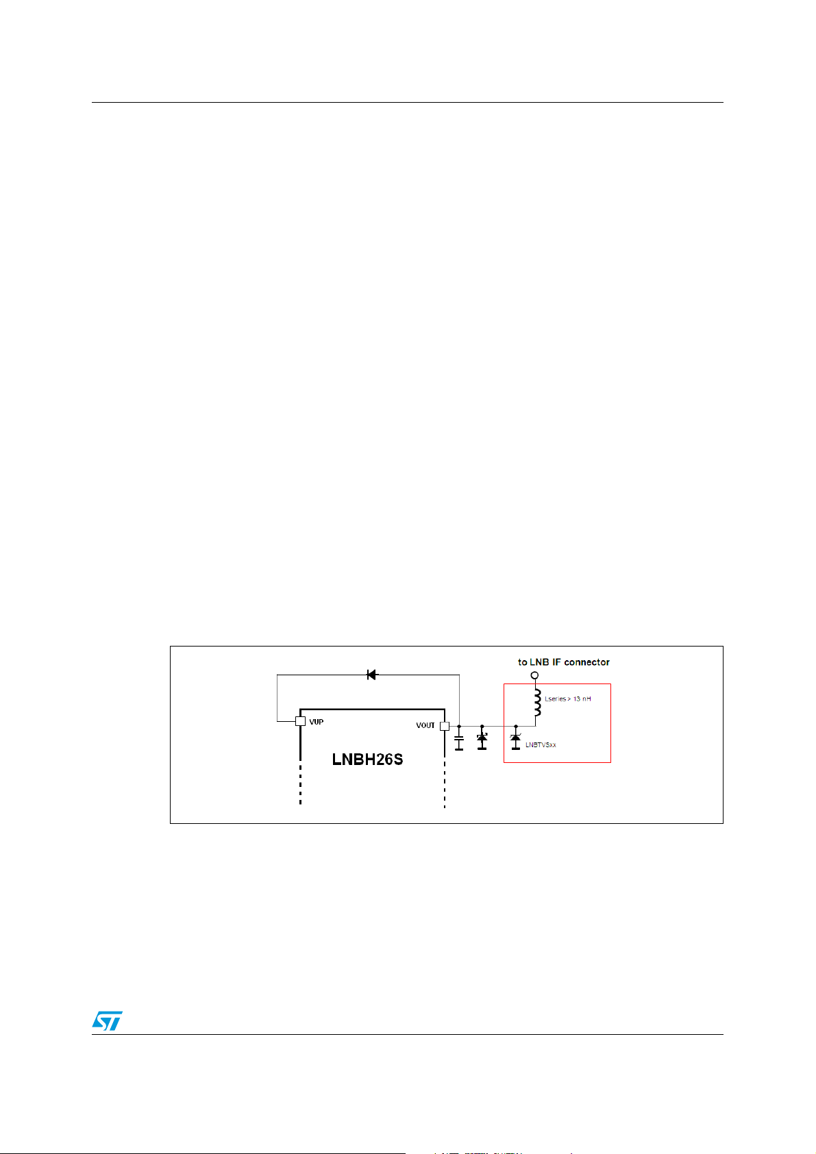
causing high voltage or current transients. Transient voltage suppressor (TVS) devices are
usually placed, as shown in the following schematic, to protect each section of STB output
circuits where the LNBH26S and other devices are electrically connected to the antenna
cable.
Figure 4. Surge protection circuit
For this purpose the use of LNBTVSxx surge protection diodes specifically designed by ST
is recommended. The selection of the LNBTVS diode should be made based on the
maximum peak power dissipation that the diode is capable of supporting (see the LNBTVS
datasheet for further details).
Doc ID 022995 Rev 1 7/29
Page 8

Application information (valid for each section A/B) LNBH26S
2.8 Power-on I²C interface reset and undervoltage lockout
The I²C interface built into the LNBH26S is automatically reset at power-on. As long as the
V
stays below the undervoltage lockout (UVLO) threshold (4.7 V typ.), the interface does
CC
not respond to any I²C command and all DATA register bits are initialized to zeroes,
therefore keeping the power blocks disabled. Once the V
rises above 4.8 V typ., the I²C
CC
interface becomes operative and the DATA registers can be configured by the main
microprocessor.
2.9 PNG: input voltage minimum detection
When input voltage (VCC pin) is lower than LPD (low power diagnostic) minimum
thresholds, the PNG I²C bit is set to “1”. Refer to the electrical characteristics table for
threshold details.
2.10 OLF: overcurrent and short-circuit protection and diagnostic
In order to reduce the total power dissipation during an overload or a short-circuit condition,
each section of the device is provided with a dynamic short-circuit protection. It is possible to
set the short-circuit current protection either statically (simple current clamp) or dynamically
through the corresponding PCL bit of the I²C DATA3 register. When the PCL (pulsed current
limiting) bit is set lo LOW, the overcurrent protection circuit works dynamically: as soon as
an overload is detected, the output current is provided for T
output is set in shutdown for a T
time of typically 900 ms. Simultaneously, the
OFF
corresponding diagnostic OLF I²C bit of the STATUS1 register is set to “1”. After this time
has elapsed, the involved output is resumed for a time T
overload is still detected, the protection circuit cycles again through T
end of a full T
in which no overload is detected, normal operation is resumed and the OLF
ON
diagnostic bit is reset to low after register reading is done. Typical T
and is determined by an internal timer. This dynamic operation can greatly reduce the power
dissipation in short-circuit condition, while still ensuring excellent power-on startup in most
conditions. However, there may be some cases in which a highly capacitive load on the
output can cause a difficult startup when the dynamic protection is chosen. This can be
solved by initiating any power startup in static mode (PCL=1) and, then, switching to the
dynamic mode (PCL=0) after a chosen amount of time depending on the output
capacitance. Also in static mode, the diagnostic OLF bit goes to “1” (and the FLT pin is set to
low) when the current clamp limit is reached and returns low when the overload condition is
cleared and register reading is done.
After the overload condition is removed, normal operation can be resumed in two ways,
according to the OLR I²C bit on the DATA4 register.
If OLR=1, all VSEL bits corresponding to the involved section are reset to “0” and the LNB
section output (V
pin) is disabled. To re-enable the output stage, the VSEL bits must be
OUT
set again by the microprocessor and the OLF bit is reset to “0” after a register reading
operation.
If OLR=0, the involved output is automatically re-enabled as soon as the overload condition
is removed, and OLF bit is reset to “0” after a register reading operation.
time 90 ms and after that, the
ON
. At the end of TON, if the
ON
and TON. At the
OFF
+ T
ON
OFF
time is 990 ms
8/29 Doc ID 022995 Rev 1
Page 9

LNBH26S Application information (valid for each section A/B)
2.11 OTF: thermal protection and diagnostic
The LNBH26S is also protected against overheating: when the junction temperature
exceeds 150 °C (typ.), the step-up converter and both linear regulators are shut off, the
diagnostic OTF bit in the STATUS1 register is set to “1”. After the overtemperature condition
is removed, normal operation can be resumed in two ways, according to the THERM I²C bit
on the DATA4 register.
If THERM=1, all VSEL bits are reset to “0” and both LNB outputs (V
To re-enable the output stages, the VSEL bits must be set again by the microprocessor,
while the OTF bit is reset to “0” after a register reading operation.
If THERM=0, outputs are automatically re-enabled as soon as the overtemperature
condition is removed, while the OTF bit is reset to “0” after a register reading operation.
pins) are disabled.
OUT
Doc ID 022995 Rev 1 9/29
Page 10
Pin configuration LNBH26S
3 Pin configuration
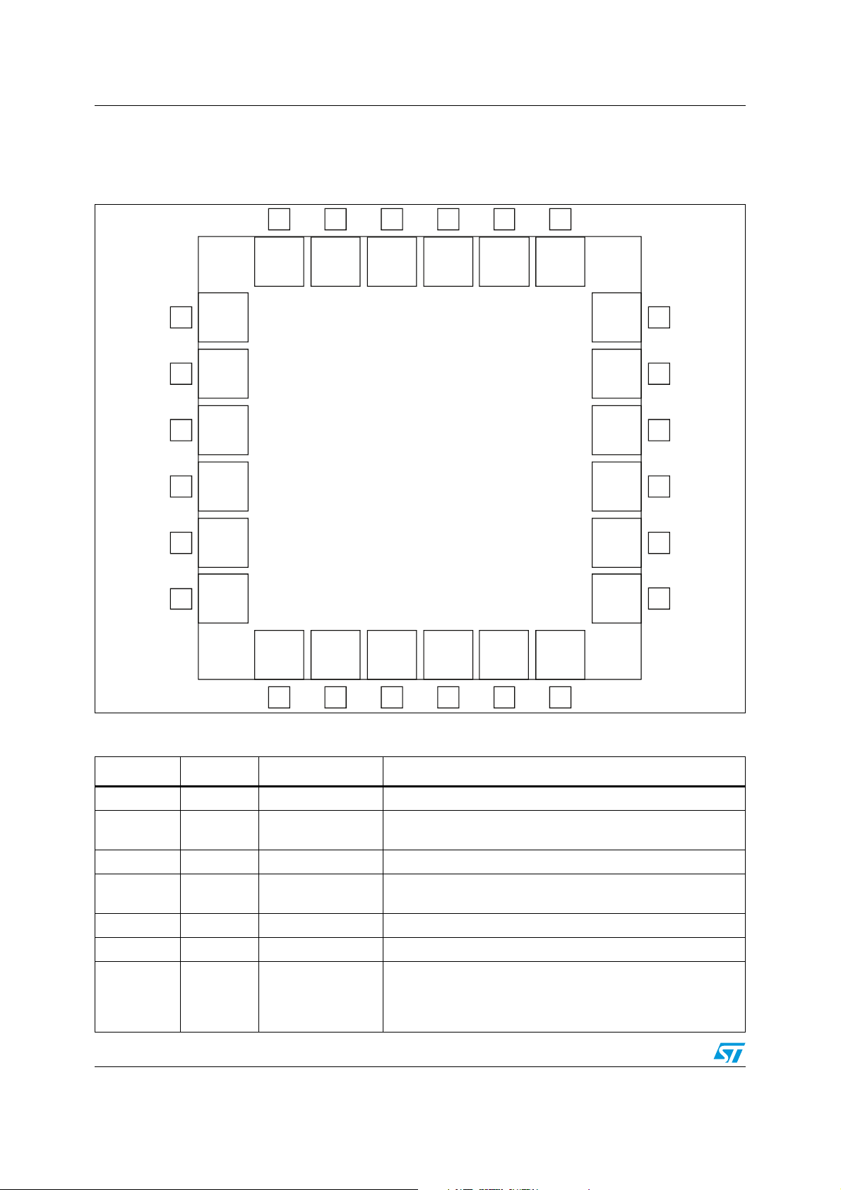
Figure 5. Pin connections (top view)
192021222324
GNDDSQIN-B DSQIN-A
GND
1
GND
2
LX-A
3
PGND
4
LX-B
5
ADDR GND
6
SCL
SDA
ISEL
VUP-A
VOUT-A
VUP-B
GND
VOUT-BNC
GND
VCC
BYP
GND
GND
18
17
16
15
14
13
7 8 9 121110
Table 2. Pin description
Pin n° Symbol Name Pin function
3 LX-A N-Mos drain Channel A, integrated N-channel Power MOSFET drain.
4 P-GND Power ground
5 LX-B N-Mos drain Channel B, integrated N-channel Power MOSFET drain.
6 ADDR Address setting
7 SCL Serial clock Clock from I²C bus.
8 SDA Serial data Bi-directional data from/to I²C bus.
Current selection for
9 ISEL
both channel A and
B
10/29 Doc ID 022995 Rev 1
DC-DC converter power ground. To be connected directly to the
Epad.
Two I²C bus addresses available by setting the Address pin
level voltage. See the Address pin characteristics table.
The resistor “RSEL” connected between ISEL and GND defines
the linear regulator current limit threshold. Refer to “output
current limit selection”
Section 2
. The RSEL resistor defines the
same current limit both for channels A and B.
AM11885v1
Page 11
LNBH26S Pin configuration
Table 2. Pin description (continued)
Pin n° Symbol Name Pin function
1, 2, 13, 14,
15, 18, 19, 23
10 N.C.
11 V
12 V
GND Analog ground Analog circuits ground. To be connected directly to the Epad.
Not internally
connected
UP-B
Channel B
step-up voltage
Channel B,
OUT-B
LNB output port
16 BYP Bypass capacitor
17 V
20 V
21 V
CC
OUT-A
UP-A
Supply input 8 to 16 V IC DC-DC power supply.
Channel A,
LNB output port
Channel A
step-up voltage
DSQIN for DiSEqC
envelope input
22 DSQIN-A
external 22 KHz TTL
DSQIN for DiSEqC
envelope Input
24 DSQIN-B
external 22 KHz TTL
or
input
or
input
Not internally connected pin. Set floating if not used.
Input of channel B linear post-regulator. The voltage on this pin
is monitored by the internal channel B step-up controller to
keep a minimum dropout across the linear pass transistor.
Output of channel B integrated very low-drop linear regulator.
Refer to
Ta b l e 1 3
for voltage selection and description.
Needed for internal pre-regulator filtering. The BYP pin is
intended only to connect an external ceramic capacitor. Any
connection of this pin to an external current or voltage sources
may cause permanent damage to the device.
Output of channel A integrated very low-drop linear regulator.
Refer to
Ta bl e 1 3
for voltage selection and description.
Input of channel A linear post-regulator. The voltage on this pin
is monitored by the internal channel A step-up controller to
keep a minimum dropout across the linear pass transistor.
It is intended for channel A 22 kHz tone control.
It can be used as DiSEqC envelope input or external 22 kHz
TTL input depending on the EXTM-A I²C bit setting as follows:
If EXTM-A=0, TEN-A=1: it accepts the DiSEqC envelope code
from the main microcontroller. The LNBH26S uses this code to
modulate the internally generated 22 kHz carrier.
If EXTM-A=TEN-A=1: it accepts external 22 kHz logic signals
which activate the 22 kHz tone output (refer to
high if the tone output is activated only by the TEN-A
Pull up
Section 2.2
).
I²C bit.
It is intended for channel B 22 kHz tone control.
It can be used as DiSEqC envelope input or external 22 kHz
TTL input depending on the EXTM-B I²C bit setting as follows:
If EXTM-B=0, TEN-B=1: it accepts the DiSEqC envelope code
from the main microcontroller. The LNBH26S uses this code to
modulate the internally generated 22 kHz carrier.
If EXTM-A=TEN-A=1: it accepts external 22 kHz logic signals
which activate the 22 kHz tone output (refer to
Section 2.2
).
Pull up high if the tone output is activated only by TEN-B I²C
bit.
Epad Epad Exposed pad
To be connected with power grounds and to the ground layer
through vias to dissipate the heat.
Doc ID 022995 Rev 1 11/29
Page 12
Maximum ratings LNBH26S
4 Maximum ratings
Table 3. Absolute maximum ratings
Symbol Parameter Value Unit
V
V
I
V
CC
UP
OUT
OUT
V
DC power supply input voltage pins -0.3 to 20 V
DC input voltage -0.3 to 40 V
Output current Internally limited mA
DC output pin voltage -0.3 to 40 V
Logic input pin voltage (SDA, SCL, DSQIN, ADDR pins) -0.3 to 7 V
I
LX LX input voltage -0.3 to 30 V
V
BYP
Internal reference pin voltage -0.3 to 4.6 V
ISEL Current selection pin voltage -0.3 to 3.5 V
T
STG
T
ESD
Storage temperature range -50 to 150 °C
Operating junction temperature range -25 to 125 °C
J
ESD rating with human body model (HBM) all pins, unless power output
pins
2
ESD rating with human body model (HBM) for power output pins 4
Table 4. Thermal data
Symbol Parameter Value Unit
thJC Thermal resistance junction-case 2 °C/W
R
kV
thJA
R
Thermal resistance junction-ambient with device soldered on 2s2p 4layer PCB provided with thermal vias below the exposed pad.
40 °C/W
Note: Absolute maximum ratings are those values beyond which damage to the device may occur.
These are stress ratings only and functional operation of the device at these conditions is
not implied. Exposure to absolute-maximum-rated conditions for extended periods may
affect device reliability. All voltage values are with respect to the network ground terminal.
12/29 Doc ID 022995 Rev 1
Page 13

LNBH26S Typical application circuits
5 Typical application circuits
Figure 6. LNBH26S DiSEqC 1.X typical application circuit
D2-A
LNBOUT -A
V
21
V
UP-A
OUT- A
20
Vin
12V
D1-A
L1-A
C1
L1-B
D1-B
C2-B
C2-A
R1 (R SEL)
C3-A
C7
C4
I2C Bus
C3-B
3
LX-A
9
ISEL
16
Byp
17
Vcc
8
SDA
{
7
SCL
5
LX-B
11
V
UP-B
LNBH26S
P-GND A-GND
4
15
D2-B
DSQIN-A
DSQIN-B
V
Table 5. LNBH26S DiSEqC 1.x bill of material
Component Notes
ADDR
OUT- B
D3-A
C5-A
22
24
6
12
To ne en able control
DiSEq C
22KHz TTL
DiSEqC
Envel ope TTL
or
LNBOUT -B
C5-B
D3-B
AM11886v1
R1 (RSEL) SMD resistor. Refer to I
current limit selection resistor values.
MAX
C1, C2 > 25 V electrolytic capacitor, 100 µF is suitable.
C3 From 470 nF to 2.2 µF ceramic capacitor. Higher values allow lower DC-DC noise.
C5 From 100 nF to 220 nF ceramic capacitor. Higher values allow lower DC-DC noise.
C4, C7 220 nF ceramic capacitors.
D1, D3 STPS130A or similar Schottky diode.
D2 1N4001-07, S1A-S1M, or any similar general purpose rectifier.
L1 10 µH inductor with I
sat
> I
peak
where I
is the boost converter peak current.
peak
Doc ID 022995 Rev 1 13/29
Page 14

I²C bus interface LNBH26S
6 I²C bus interface
Data transmission from the main microprocessor to the LNBH26S, and vice versa, takes
place through the 2-wire I²C bus interface, consisting of the 2-line SDA and SCL (pull-up
resistors to positive supply voltage must be externally connected).
6.1 Data validity
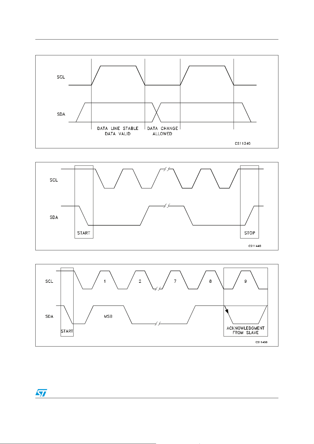
As shown in
of the clock. The high and low state of the data line can only change when the clock signal
on the SCL line is LOW.
Figure 7
, the data on the SDA line must be stable during the high semi-period
6.2 START and STOP condition
As shown in
SCL is HIGH. The STOP condition is a low to high transition of the SDA line while SCL is
HIGH. A STOP condition must be sent before each START condition.
Figure 8
, a START condition is a high to low transition of the SDA line while
6.3 Byte format
Every byte transferred to the SDA line must contain 8 bits. Each byte must be followed by an
acknowledge bit. The MSb is transferred first.
6.4 Acknowledge
The master (microprocessor) puts a resistive high level on the SDA line during the
acknowledge clock pulse (see
must pull down (LOW) the SDA line during the acknowledge clock pulse, so that the SDA
line is stable low during this clock pulse. The peripheral which has been addressed must
generate an acknowledge after the reception of each byte, otherwise the SDA line remains
at the high level during the ninth clock pulse time. In this case the master transmitter can
generate the STOP information in order to abort the transfer. The LNBH26S won't generate
acknowledge if the V
supply is below the undervoltage lockout threshold (4.7 V typ.).
CC
Figure 9
). The peripheral (LNBH26S) which acknowledges
6.5 Transmission without acknowledge
If the detection of LNBH26S acknowledge is not necessary, the microprocessor can use a
simpler transmission; it simply waits one clock without checking the slave acknowledging,
and sends the new data. This approach is of course less protected from misworking and
decreases noise immunity.
14/29 Doc ID 022995 Rev 1
Page 15
LNBH26S I²C bus interface
Figure 7. Data validity on the I²C bus
Figure 8. Timing diagram of I²C bus
Figure 9. Acknowledge on the I²C bus
Doc ID 022995 Rev 1 15/29
Page 16
I²C interface protocol LNBH26S
7 I²C interface protocol
7.1 Write mode transmission
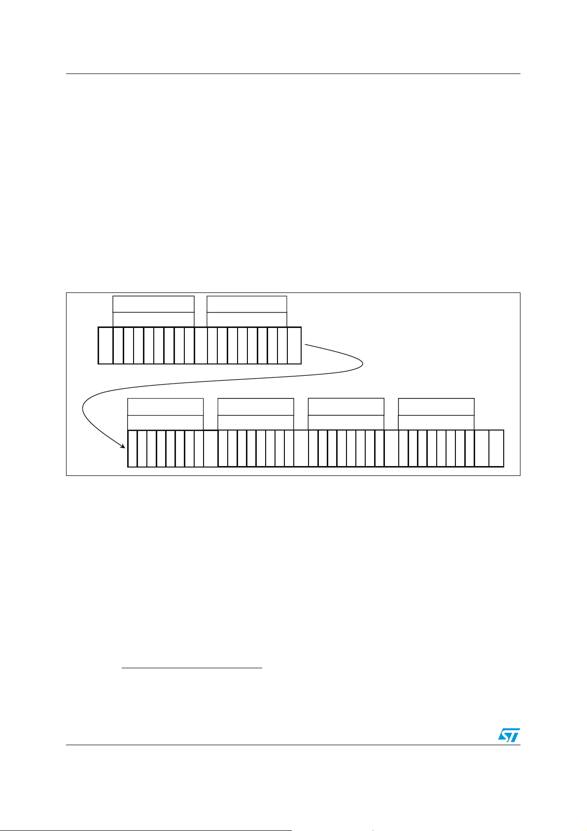
The LNBH26S interface protocol is made up of:
● a START condition (S)
● a chip address byte with the LSb bit R/W = 0
● a register address (internal address of the first register to be accessed)
● a sequence of data (byte to write in the addressed internal register + acknowledge)
● the following bytes, if any, to be written in successive internal registers
● a STOP condition (P), the transfer lasts until a stop bit is encountered
● the LNBH26S, as slave, acknowledges every byte transfer.
Figure 10. Example of writing procedure starting with first data address 0x2
CHIP ADDRESS
MSB
S 000100X
DATA 1
Add=0x2
MSB LSB
VSEL4-B
VSEL3-B
VSEL2-B
VSEL1-B
VSEL4-A
VSEL3-A
LSB
REGISTER ADDRESS
MSB
R/W = 0
ACK
00000XXX
MSB LSB
VSEL2-A
VSEL1-A
ACK
N/A
EXTM-B
DATA 2
Add=0x3
TEN-B
N/A
N/A
LSB
ACK
DATA 3
Add=0x4
MSB LSB
EXTM-A
TEN-A
N/A
ACK
N/A
PCL-B
N/A
N/A
N/A
-A
PCL
N/A
N/A
ACK
DATA 4
Add=0x5
MSB LSB
THERM
N/A
N/A
N/A
ACK = Acknowledge
S = Start
P = Stop
R/W = 1/0, read/write bit
X = 0/1, set the values to select the chip address (see
select the register address (see
Ta bl e 6
to
Ta bl e 1 1
).
Ta b le 1 5
for pin selection) and to
OLR
N/A
N/A
N/A
(a)
ACK
P
AM10485v1
a. The writing procedure can start from any register address by simply setting the X values in the register address
byte (after the chip address). It can be also stopped from the master by sending a STOP condition after any
acknowledge bit.
16/29 Doc ID 022995 Rev 1
Page 17
LNBH26S I²C interface protocol
7.2 Read mode transmission
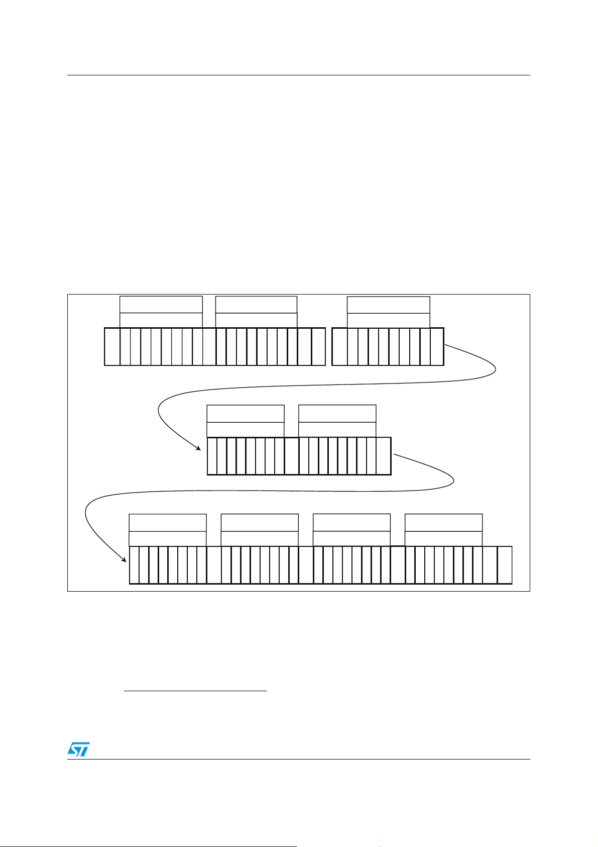
In read mode the bytes sequence must be as follows:
● a START condition (S)
● a chip address byte with the LSb bit R/W=0
● the register address byte of the internal first register to be accessed
● a STOP condition (P)
● a new master transmission with the chip address byte and the LSb bit R/W=1
● after the acknowledge, the LNBH26S starts to send the addressed register content. As
long as the master keeps the acknowledge LOW, the LNBH26S transmits the next
address register byte content.
● the transmission is terminated when the master sets the acknowledge high with a
following stop bit.
Figure 11. Example of reading procedure starting with first status address 0X0
CHIP ADDRESS
MSB
S 000100X
DATA 1
Add=0x2
MSB LSB
VSEL4-B
VSEL3-B
VSEL2-B
VSEL1-B
VSEL4-A
VSEL3-A
LSB
VSEL2-A
REGISTER ADDRESS
MSB
R/W = 0
ACK
00000XXX
STATUS 1
Add=0x0
MSB LSB
PNG
OTF
N/A
N/A
MSB LSB
VSEL1-A
ACK
N/A
EXTM-B
N/A
N/A
N/A
DATA 2
Add=0x3
TEN-B
N/A
OLF-B
OLF-A
EXTM-A
LSB
ACK
P
STATUS 2
Add= 0x1
MSB LSB
ACK
N/A
N/A
N/A
MSB LSB
ACK
N/A
PCL-B
N/A
TEN-A
CHIP ADDRESS
MSB
S000100X
N/A
N/A
ACK
N/A
PCL-A
N/A
N/A
ACK
N/A
N/A
N/A
N/A
DATA 3
Add=0x4
N/A
LSB
R/W = 1
ACK
DATA 4
Add= 0x5
MSB LSB
THERM
N/A
N/A
OLR
N/A
N/A
N/A
N/A
(b)
ACK
P
AM10486v1
ACK = Acknowledge
S = Start
P = Stop
R/W = 1/0, read/write bit
X = 0/1, set the values to select the chip address (see
select the register address (see
b. The reading procedure can start from any register address (Status 1, 2 or Data1..4) by simply setting the X
values in the register address byte (after the first chip address in the above figure). It can be also stopped from
the master by sending a STOP condition after any acknowledge bit.
Ta bl e 6
to
Ta bl e 1 1
Doc ID 022995 Rev 1 17/29
).
Ta b le 1 5
for pin selection) and to
Page 18
I²C interface protocol LNBH26S
7.3 Data registers
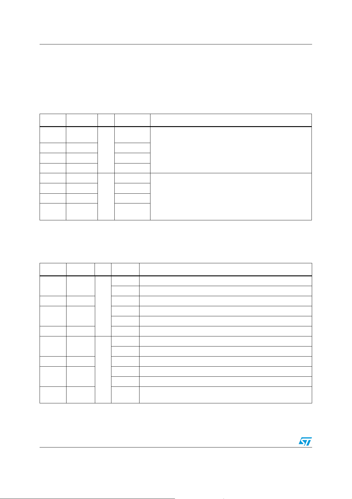
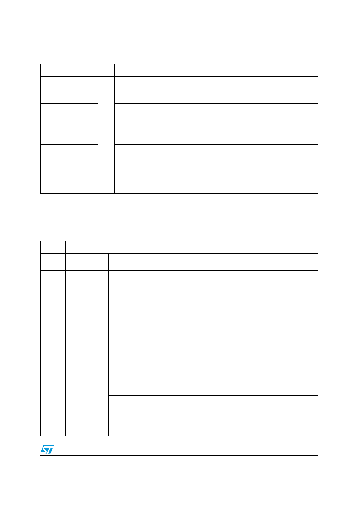
The DATA 1..4 registers can be addressed both in write and read mode. In read mode they
return the last writing byte status received in the previous write transmission.
The following tables provide the register address values of Data 1..4 and a function
description of each bit.
Table 6. DATA 1 (read/write register. Register address = 0X2)
Bit Name CH Value Description
Bit 0
(LSb)
Bit 1 VSEL2-A 0/1
Bit 2 VSEL3-A 0/1
Bit 3 VSEL4-A 0/1
Bit 4 VSEL1-B
Bit 5 VSEL2-B 0/1
Bit 6 VSEL3-B 0/1
Bit 7
(MSb)
VSEL1-A
A
B
VSEL4-B 0/1
0/1
0/1
output voltage selection bits.
(Refer to
output voltage selection bits.
(Refer to
N/A = Reserved bit.
All bits reset to “0” at power-on.
Table 7. DATA 2 (read/write register. Register address = 0X3)
Bit Name CH Value Description
Bit 0
(LSb)
Bit 1 N/A 0 Reserved. Keep to “0”.
Bit 2 EXTM-A
1 22 kHz tone enabled. Tone output controlled by the DSQIN pin
TEN-A
0 22 kHz tone output disabled
A
1 DSQIN input pin is set to receive external 22 kHz TTL signal source
0 DSQIN input pin is set to receive external DiSEqC envelope TTL signal
Channel A
Ta bl e 1 3
Channel B
Ta bl e 1 3
)
)
Bit 3 N/A 0 Reserved. Keep to “0”.
Bit 4 TEN-B
Bit 5 N/A 0 Reserved. Keep to “0”.
B
Bit 6 EXTM-B
Bit 7
(MSb)
N/A 0 Reserved. Keep to “0”.
1 22 kHz tone enabled. Tone output controlled by the DSQIN pin
0 22 kHz tone output disabled
1 DSQIN input pin is set to receive external 22 kHz TTL signal source
0 DSQIN input pin is set to receive external DiSEqC envelope TTL signal
N/A = Reserved bit.
All bits reset to “0” at power-on.
18/29 Doc ID 022995 Rev 1
Page 19
LNBH26S I²C interface protocol
Table 8. DATA 3 (read/write register. Register address = 0X4)
Bit Name CH Value Description
Bit 0
(LSb)
N/A
0 Reserved. Keep to “0”
Bit 1 N/A 0 Reserved. Keep to “0”
Bit 2 PCL-A 1 Pulsed (Dynamic) LNB output current limiting is deactivated
A
0 Pulsed (Dynamic) LNB output current limiting is activated
Bit 3 N/A 0 Reserved. Keep to “0”
Bit 4 N/A
0 Reserved. Keep to “0”
Bit 5 N/A 0 Reserved. Keep to “0”
Bit 6 PCL-B 1 Pulsed (Dynamic) LNB output current limiting is deactivated
B
0 Pulsed (Dynamic) LNB output current limiting is activated
Bit 7
(MSb)
N/A 0 Reserved. Keep to “0”
N/A = Reserved bit.
All bits reset to “0” at power-on.
Table 9. DATA 4 (read/write register. Register address = 0X5)
Bit Name CH Value Description
Bit 0
(LSb)
Bit 1 N/A - 0 Reserved. Keep to “0”.
Bit 2 N/A - 0 Reserved. Keep to “0”.
Bit 3 OLR A/B
Bit 4 N/A - 0 Reserved. Keep to “0”.
Bit 5 N/A - 0 Reserved. Keep to “0”.
Bit 6 THERM A/B
N/A - 0 Reserved. Keep to “0”.
In the case of overload protection activation (OLF=1), all VSEL 1..4 bits
1
are reset to “0” and LNB output (V
must be set again by the master after the overcurrent condition is
removed (OLF=0).
In the case of overload protection activation (OLF=1) the LNB output
0
(V
pin) is automatically enabled as soon as the overload condition is
OUT
removed (OLF=0) with the previous VSEL bits setting.
If thermal protection is activated (OTF=1), all VSEL 1..4 bits are reset to
1
“0” and LNB output (V
again by the master after the overtemperature condition is removed
(OTF=0).
In the case of thermal protection activation (OTF=1) the LNB output
0
(V
pin) is automatically enabled as soon as the overtemperature
OUT
condition is removed (OTF=0) with the previous VSEL bits setting.
pin) is disabled. The VSEL bits must be set
OUT
pin) is disabled. The VSEL bits
OUT
Bit 7
(MSb)
COMP - 0 Reserved. Keep to “0”
Doc ID 022995 Rev 1 19/29
Page 20
I²C interface protocol LNBH26S
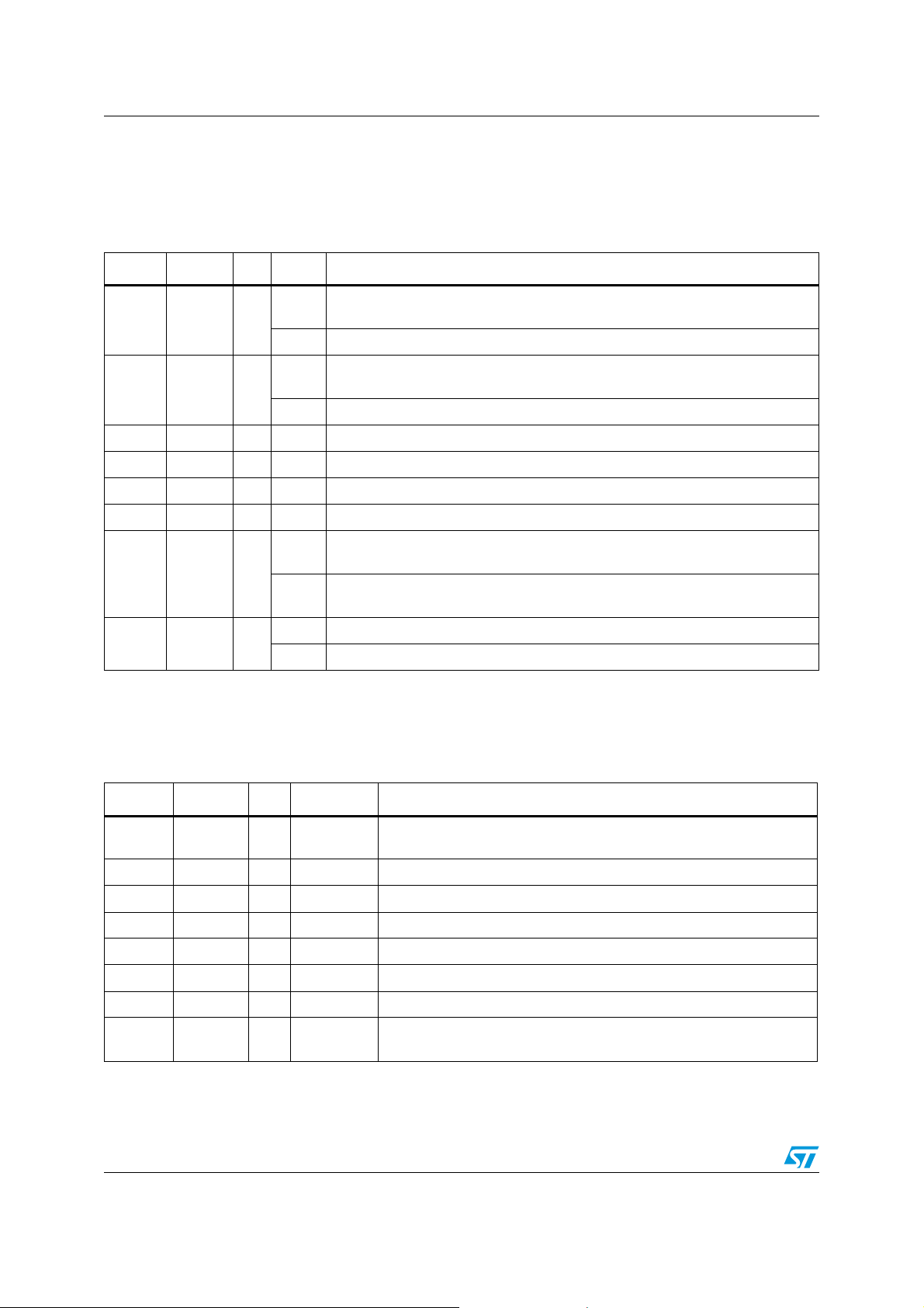
7.4 Status registers
The STATUS 1, 2 registers can be addressed only in read mode and provide the diagnostic
functions described in the following tables.
Table 10. STATUS 1 (read register. Register address = 0X0)
Bit Name CH Value Description
Bit 0
(LSb)
Bit 1 OLF-B B
Bit 2 N/A - - Reserved
Bit 3 N/A - - Reserved
Bit 4 N/A - - Reserved
Bit 5 N/A - - Reserved
Bit 6 OTF A/B
OLF-A A
V
pin overload protection has been triggered (I
OUT
1
for the overload operation and PCL settings.
0 No overload protection has been triggered to the V
V
pin overload protection has been triggered (I
OUT
1
for the overload operation and PCL settings.
0 No overload protection has been triggered to V
Junction overtemperature is detected, T
1
setting in
Junction overtemperature not detected, T
0
protection threshold.
Table 9
.
OUT
> 150 °C (typ.). See also THERM bit
J
<135 °C (typ.). TJ is below thermal
J
OUT
OUT
OUT
pin (I
> I
MAX
pin (I
> I
MAX
OUT
). Refer to
< I
OUT
MAX
). Refer to
< I
).
MAX
Ta bl e 8
).
Ta bl e 8
Bit 7
(MSb)
PNG A/B
1 Input voltage (V
0 Input voltage (V
pin) lower than LPD minimum thresholds. Refer to
CC
pin) higher than LPD thresholds. Refer to
CC
N/A = Reserved bit.
All bits reset to “0” at power-on.
Table 11. STATUS 2 (read register. Register address = 0X1)
Bit Name CH Value Description
Bit 0
(LSb)
Bit 1 N/A - - Reserved
Bit 2 N/A - - Reserved
Bit 3 N/A - - Reserved
Bit 4 N/A - - Reserved
Bit 5 N/A - - Reserved
Bit 6 N/A - - Reserved
Bit 7
(MSb)
N/A - - Reserved
N/A - - Reserved
Ta bl e 1 2
Ta bl e 1 2
.
.
N/A = Reserved bit.
All bits reset to “0” at power-on.
20/29 Doc ID 022995 Rev 1
Page 21
LNBH26S Electrical characteristics
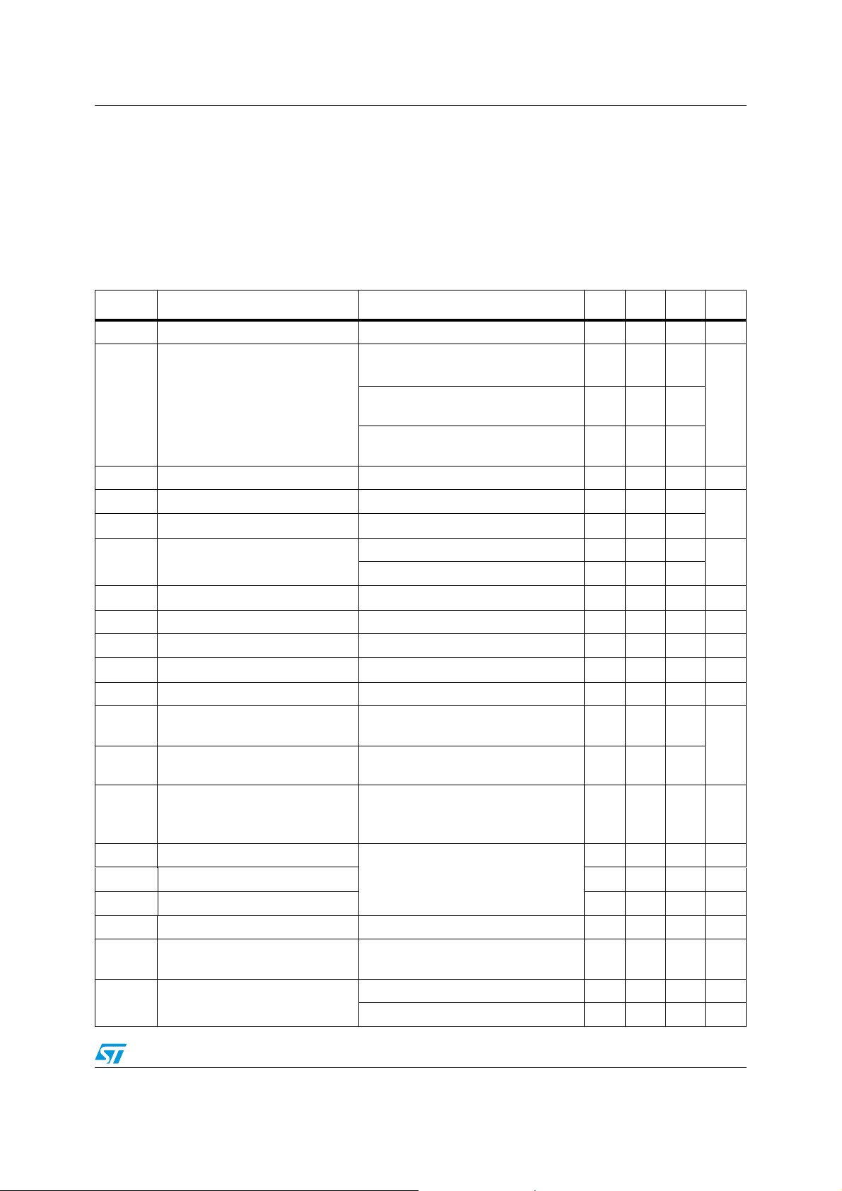
8 Electrical characteristics
Refer to
RSEL = 11 kΩ, DSQIN = LOW, V
values are referred to T
for I²C access to the system register (
Table 12. Electrical characteristics of section A/B
Section 5
, TJ from 0 to 85 °C, all DATA 1..4 register bits set to 0 unless VSEL1 = 1,
= 25 °C. V
J
= 12 V, I
IN
OUT
Section 6
= V
= 50 mA, unless otherwise stated. Typical
OUT
pin voltage. See software description section
OUT
and
Section 7
).
Symbol Parameter Test conditions Min. Typ. Max. Unit
(1)
81216V
Both sections A and B enabled,
I
= 0 mA
OUT
22 kHz tone enabled (TEN-A/B = 1,
DSQIN-A/B = High), I
OUT
= 0 mA
12
19
Both sections A and B set in standby:
VSEL1=VSEL2=VSEL3=VSEL4=0
selected level -3.5 +3.5 %
OUT
= 8 to 16 V 40
IN
from 50 to 500 mA 75 100
OUT
2
V
V
V
V
I
OUT
OUT
OUT
Supply voltage
IN
Supply current
IN
Output voltage total accuracy Valid at any V
Line regulation V
Load regulation I
RSEL = 15 kΩ 500 750
I
MAX
I
SS Soft-start time V
SS Soft-start time V
T13-18 Soft transition rise time V
T18-13 Soft transition fall time V
T
T
Output current limiting thresholds
RSEL = 20 kΩ 350 550
Output short-circuit current RSEL = 15 kΩ 350 mA
SC
from 0 to 13 V 4 ms
OUT
from 0 to 18 V 6 ms
OUT
from 13 to 18 V 1.5 ms
OUT
from 18 to 13 V 1.5 ms
OUT
Dynamic overload protection OFF
OFF
time
Dynamic overload protection ON
ON
time
PCL = 0, output shorted 900
T
PCL = 0, output shorted
OFF
10
/
mA
mV
mA
ms
A
TONE
F
TONE
D
TONE
tr, tf Tone rise or fall time
Eff
DC/DC
F
Tone amplitude
Tone frequency
Tone duty cycle 43 50 57 %
(2)
DC-DC converter efficiency I
DC-DC converter switching
SW
frequency
UVLO Undervoltage lockout thresholds
DSQIN=High, EXTM=0, TEN=1
from 0 to 500 mA
I
OUT
from 0 to 750 nF
C
BUS
0.55 0.675 0.8 V
PP
20 22 24 kHz
DSQIN=High, EXTM=0, TEN=1
5 8 15 µs
= 500 mA 93 %
OUT
440 kHz
UVLO threshold rising 4.8 V
UVLO threshold falling 4.7
Doc ID 022995 Rev 1 21/29
Page 22
Electrical characteristics LNBH26S
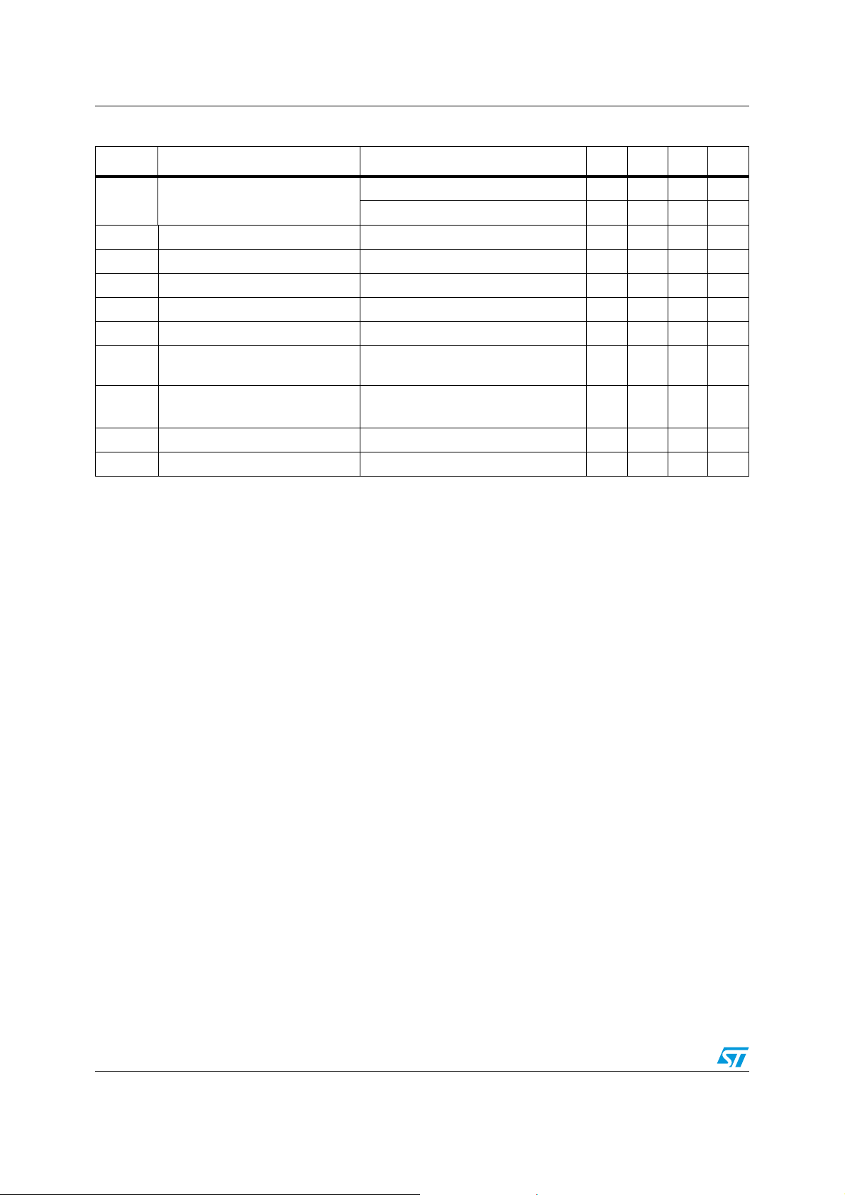
Table 12. Electrical characteristics of section A/B (continued)
Symbol Parameter Test conditions Min. Typ. Max. Unit
threshold rising 7.2 V
V
V
V
V
I
OBK
I
SINK
I
SINK_TIM
E-OUT
I
REV
T
SHDN
ΔT
1. In applications where (VCC - V
account in the application thermal management design.
2. Guaranteed by design.
Low power diagnostic (LPD)
LP
thresholds
DSQIN, pin logic low 0.8 V
IL
DSQIN, pin logic high 2 V
IH
I
DSQIN, pin input current V
IH
Output backward current All VSELx = 0, V
Output low-side sink current V
Low-side sink current time-out V
Max. reverse current
Thermal shutdown threshold 150 °C
Thermal shutdown hysteresis 15 °C
SHDN
) > 1.3 V, the increased power dissipation inside the integrated LDO must be taken into
OUT
LP
V
threshold falling 6.7
LP
= 5 V 15 µA
IH
= 30 V -3 -6 mA
OBK
forced at V
OUT
forced at V
OUT
V
forced at V
OUT
after I
SINK_TIME-OUT
OUT_nom
OUT_nom
OUT_nom
+0.1 V 70 mA
+0.1 V 10 ms
+0.1 V,
is elapsed.
2mA
8.1 Output voltage selection
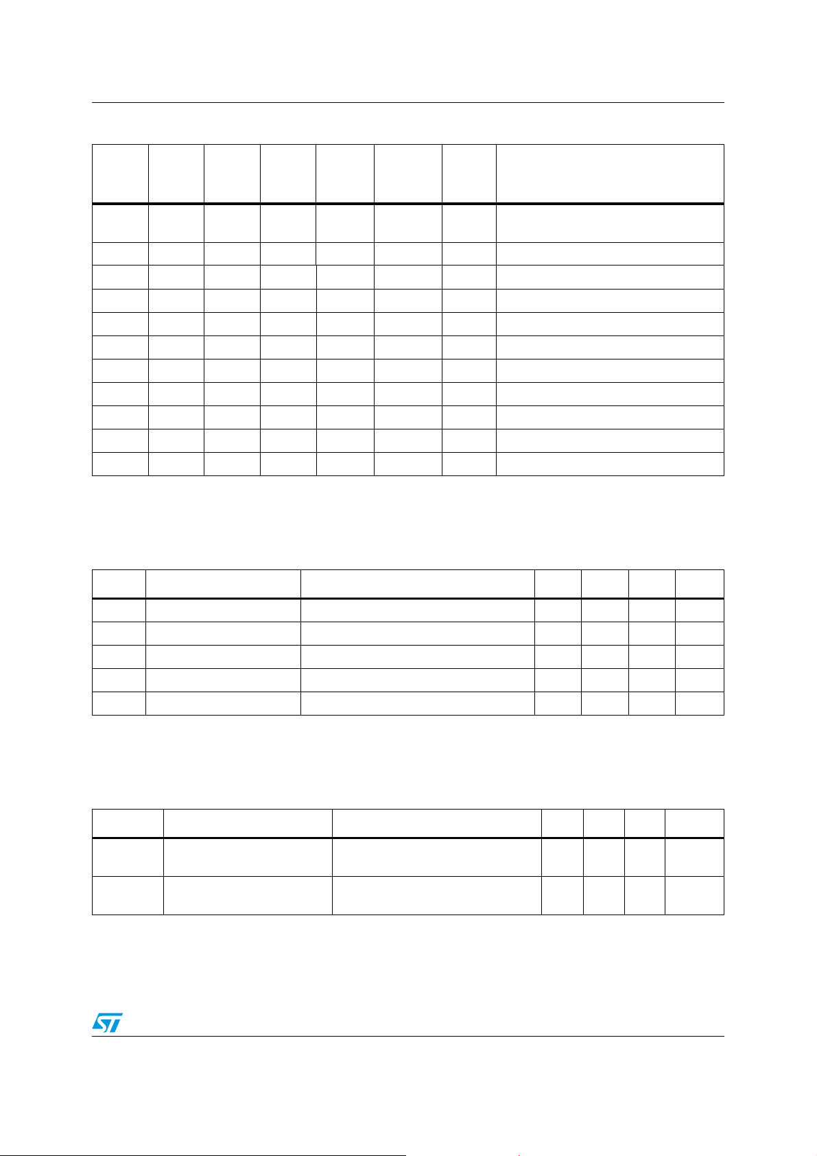
Each LNBH26S channel is provided with 8 output voltage levels (4 levels for 13 V range
when VSEL4-A/B=0 and 4 levels for 18 V range when VSEL4-A/B=1) which can be selected
through the register Data1. The following table shows the output voltage values
corresponding to VSELx bit combinations both for channel A and B. If all VSELx are at “0”
the device is set in standby mode and the V
-A/B are disabled.
OUT
22/29 Doc ID 022995 Rev 1
Page 23
LNBH26S Electrical characteristics
Table 13. Output voltage selection table (Data1 register, write mode)
VSEL4-
A/B
0000 0
VSEL3-
A/B
VSEL2-
A/B
VSEL1-
A/B
V
OUT
min.
V
OUT
pin
voltage
-A/B
V
OUT
max.
-A/B disabled. LNBH26S set in
V
OUT
standby mode
000112.54513.00013.455
001012.86713.33313.800
001113.18813.66714.145
010013.5114.00014.490
100017.51518.15018.785
100117.83618.48319.130
101018.15818.81719.475
101118.4819.15019.820
1. TJ from 0 to 85 °C, VI = 12 V.
(1)
Function
TJ from 0 to 85 °C, VI = 12 V.
Table 14. I²C electrical characteristics
Symbol Parameter Test conditions Min. Typ. Max. Unit
V
IL
V
IH
I
IN
V
OL
F
MAX
1. Guaranteed by design.
Low level input voltage SDA, SCL 0.8 V
High level input voltage SDA, SCL 2 V
Input current SDA, SCL, V
Low level output voltage
(1)
SDA (open drain), IOL = 6 mA 0.6 V
= 0.4 to 4.5 V -10 10 µA
IN
Maximum clock frequency SCL 400 kHz
TJ from 0 to 85 °C, VI = 12 V.
Table 15. Address pin characteristics
Symbol Parameter Test condition Min. Typ. Max. Unit
V
ADDR-1
V
ADDR-2
“0001000(R/W)” Address pin
voltage range
“0001001(R/W)” Address pin
voltage range
R/W bit determines the transmission
mode: read (R/W=1) write (R/W=0)
R/W bit determines the transmission
mode: read (R/W=1) write (R/W=0)
00.8V
25V
Doc ID 022995 Rev 1 23/29
Page 24
Package mechanical data LNBH26S
9 Package mechanical data
In order to meet environmental requirements, ST offers these devices in different grades of
®
ECOPACK
specifications, grade definitions and product status are available at:
packages, depending on their level of environmental compliance. ECOPACK
www.st.com
.
ECOPACK is an ST trademark.
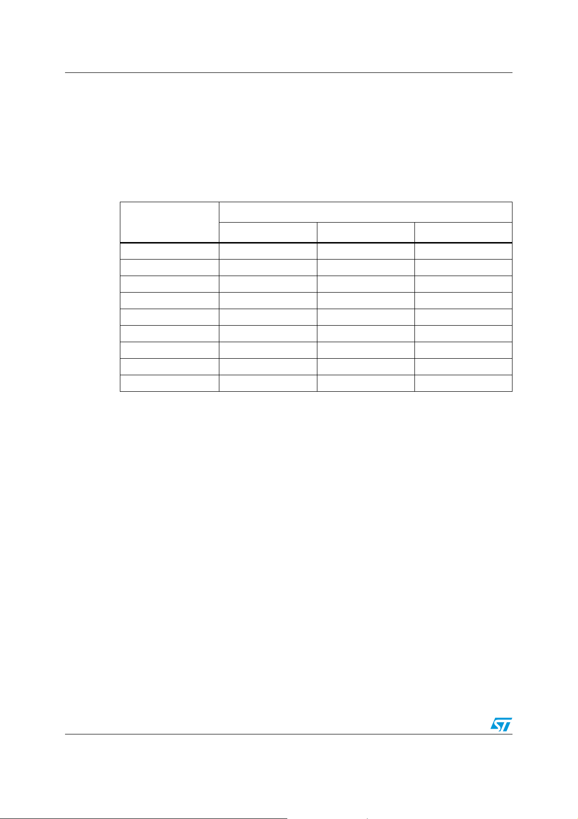
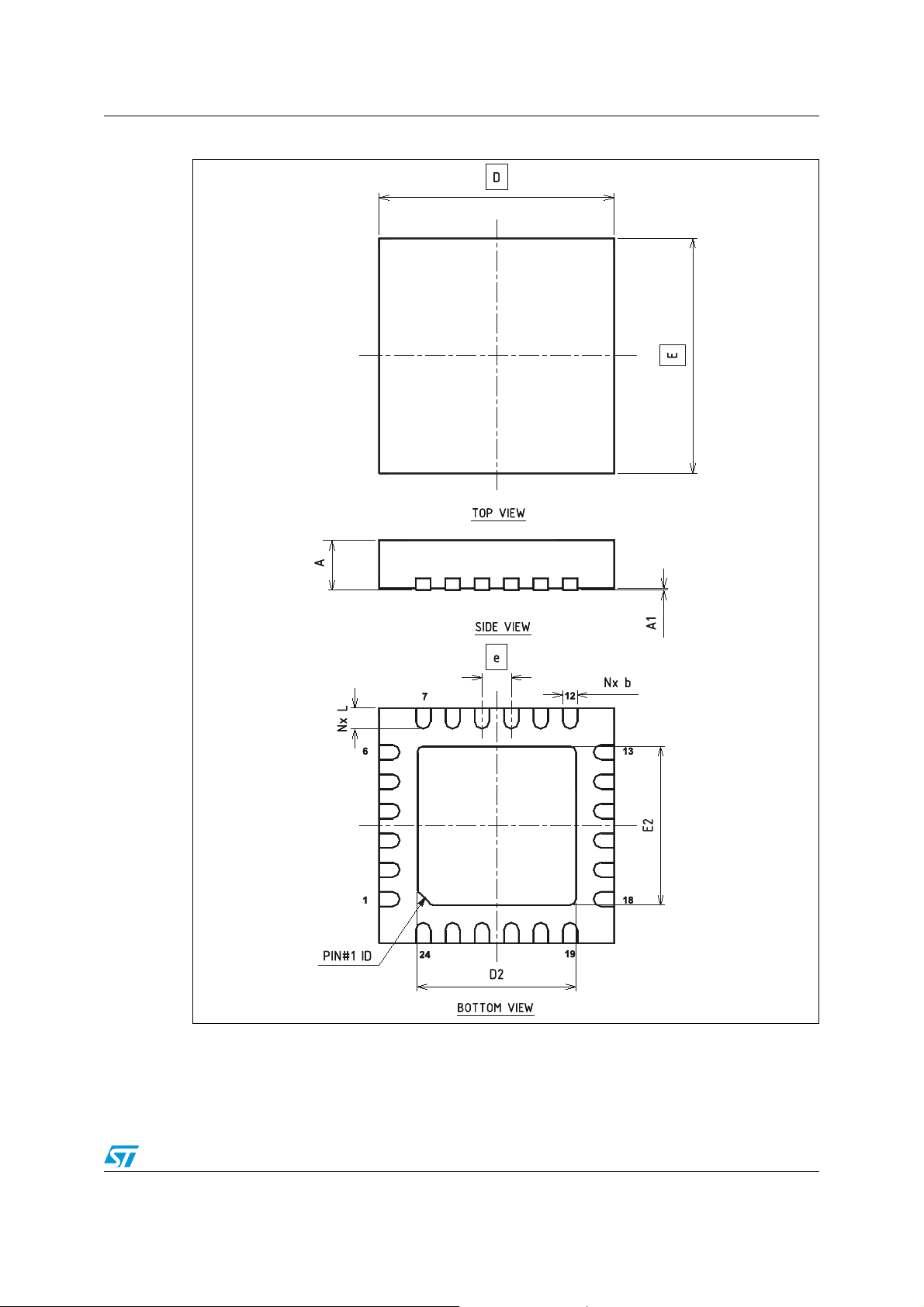
Table 16. QFN24L (4x4 mm) mechanical data
(mm)
Dim.
Min. Typ. Max.
A 0.80 0.90 1.00
A1 0.00 0.02 0.05
b 0.18 0.25 0.30
D 3.90 4.00 4.10
D2 2.55 2.70 2.80
E 3.90 4.00 4.10
E2 2.55 2.70 2.80
e 0.45 0.50 0.55
L 0.25 0.35 0.45
24/29 Doc ID 022995 Rev 1
Page 25
LNBH26S Package mechanical data
Figure 12. QFN24L (4x4 mm) package dimensions
7596209_D
Doc ID 022995 Rev 1 25/29
Page 26
Package mechanical data LNBH26S
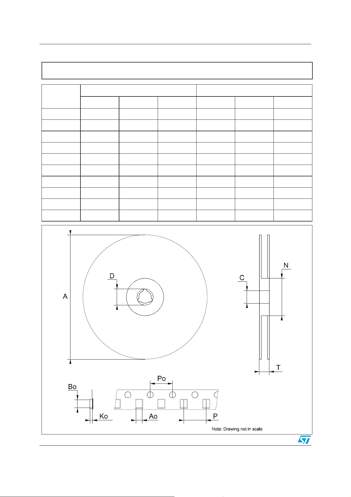
Tape & reel QFNxx/DFNxx (4x4) mechanical data
mm. inch.
Dim.
Min. Typ. Max. Min. Typ. Max.
A 330 12.992
C 12.8 13.2 0.504 0.519
D 20.2 0.795
N 99 101 3.898 3.976
T 14.4 0.567
Ao 4.35 0.171
Bo 4.35 0.171
Ko 1.1 0.043
Po 4 0.157
P 8 0.315
26/29 Doc ID 022995 Rev 1
Page 27
LNBH26S Package mechanical data
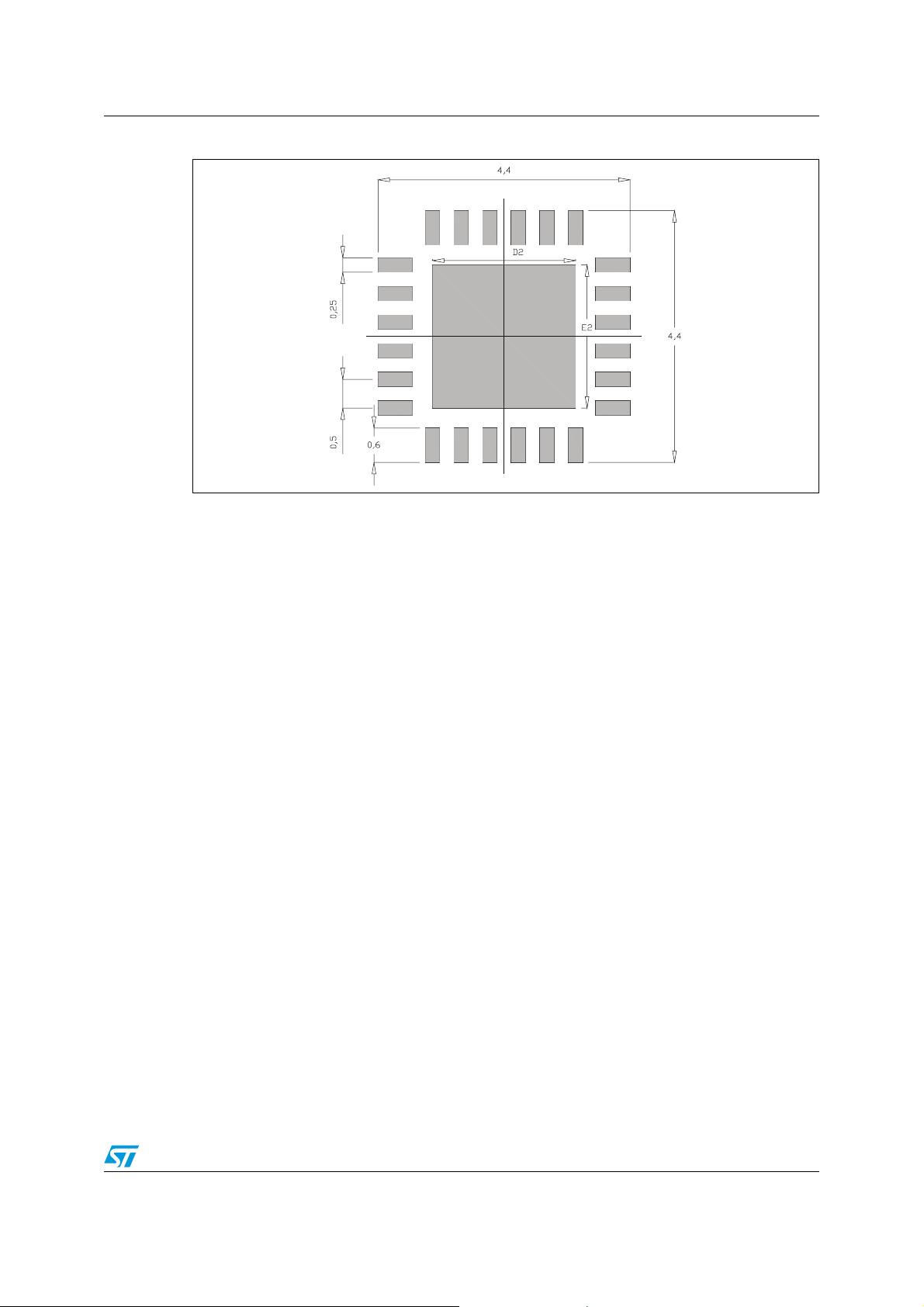
Figure 13. QFN24L (4x4) footprint recommended data (mm)
Doc ID 022995 Rev 1 27/29
Page 28
Revision history LNBH26S
10 Revision history
Table 17. Document revision history
Date Revision Changes
27-Mar-2012 1 Initial release.
28/29 Doc ID 022995 Rev 1
Page 29

LNBH26S
Please Read Carefully:
Information in this document is provided solely in connection with ST products. STMicroelectronics NV and its subsidiaries (“ST”) reserve the
right to make changes, corrections, modifications or improvements, to this document, and the products and services described herein at any
time, without notice.
All ST products are sold pursuant to ST’s terms and conditions of sale.
Purchasers are solely responsible for the choice, selection and use of the ST products and services described herein, and ST assumes no
liability whatsoever relating to the choice, selection or use of the ST products and services described herein.
No license, express or implied, by estoppel or otherwise, to any intellectual property rights is granted under this document. If any part of this
document refers to any third party products or services it shall not be deemed a license grant by ST for the use of such third party products
or services, or any intellectual property contained therein or considered as a warranty covering the use in any manner whatsoever of such
third party products or services or any intellectual property contained therein.
UNLESS OTHERWISE SET FORTH IN ST’S TERMS AND CONDITIONS OF SALE ST DISCLAIMS ANY EXPRESS OR IMPLIED
WARRANTY WITH RESPECT TO THE USE AND/OR SALE OF ST PRODUCTS INCLUDING WITHOUT LIMITATION IMPLIED
WARRANTIES OF MERCHANTABILITY, FITNESS FOR A PARTICULAR PURPOSE (AND THEIR EQUIVALENTS UNDER THE LAWS
OF ANY JURISDICTION), OR INFRINGEMENT OF ANY PATENT, COPYRIGHT OR OTHER INTELLECTUAL PROPERTY RIGHT.
UNLESS EXPRESSLY APPROVED IN WRITING BY TWO AUTHORIZED ST REPRESENTATIVES, ST PRODUCTS ARE NOT
RECOMMENDED, AUTHORIZED OR WARRANTED FOR USE IN MILITARY, AIR CRAFT, SPACE, LIFE SAVING, OR LIFE SUSTAINING
APPLICATIONS, NOR IN PRODUCTS OR SYSTEMS WHERE FAILURE OR MALFUNCTION MAY RESULT IN PERSONAL INJURY,
DEATH, OR SEVERE PROPERTY OR ENVIRONMENTAL DAMAGE. ST PRODUCTS WHICH ARE NOT SPECIFIED AS "AUTOMOTIVE
GRADE" MAY ONLY BE USED IN AUTOMOTIVE APPLICATIONS AT USER’S OWN RISK.
Resale of ST products with provisions different from the statements and/or technical features set forth in this document shall immediately void
any warranty granted by ST for the ST product or service described herein and shall not create or extend in any manner whatsoever, any
liability of ST.
ST and the ST logo are trademarks or registered trademarks of ST in various countries.
Information in this document supersedes and replaces all information previously supplied.
The ST logo is a registered trademark of STMicroelectronics. All other names are the property of their respective owners.
© 2012 STMicroelectronics - All rights reserved
STMicroelectronics group of companies
Australia - Belgium - Brazil - Canada - China - Czech Republic - Finland - France - Germany - Hong Kong - India - Israel - Italy - Japan -
Malaysia - Malta - Morocco - Philippines - Singapore - Spain - Sweden - Switzerland - United Kingdom - United States of America
www.st.com
Doc ID 022995 Rev 1 29/29
 Loading...