

Page 1
LM7705
+
-
C
RES
C
FLY
C
OUT
+ In
- In
shutdown
low voltage
amplifier
true zero
output voltage
-V
+V
+V
-0.23V
C
F+
V
SS
SD
V
DD
V
SS
V
OUT
C
RES
C
F-
Product
Folder
Order
Now
Technical
Documents
Tools &
Software
Support &
Community
SNVS420D –NOVEMBER 2008–REVISED MAY 2018
LM7705 Low-Noise Negative Bias Generator
LM7705
1 Features
1
• Regulated Output Voltage −0.232 V
• Output Voltage Tolerance 5%
• Output Voltage Ripple 4 mV
PP
• Supply Voltage 3 V to 5.25 V
• Conversion Efficiency Up to 98%
• Quiescent Current 78 µA
• Shutdown Current 20 nA
• Turnon Time 500 µs
• Operating Temperature Range −40°C to 125°C
• 8-Pin VSSOP Package
2 Applications
• True Zero Amplifier Outputs
• Portable Instrumentation
• Low-Voltage Split-Power Supplies
3 Description
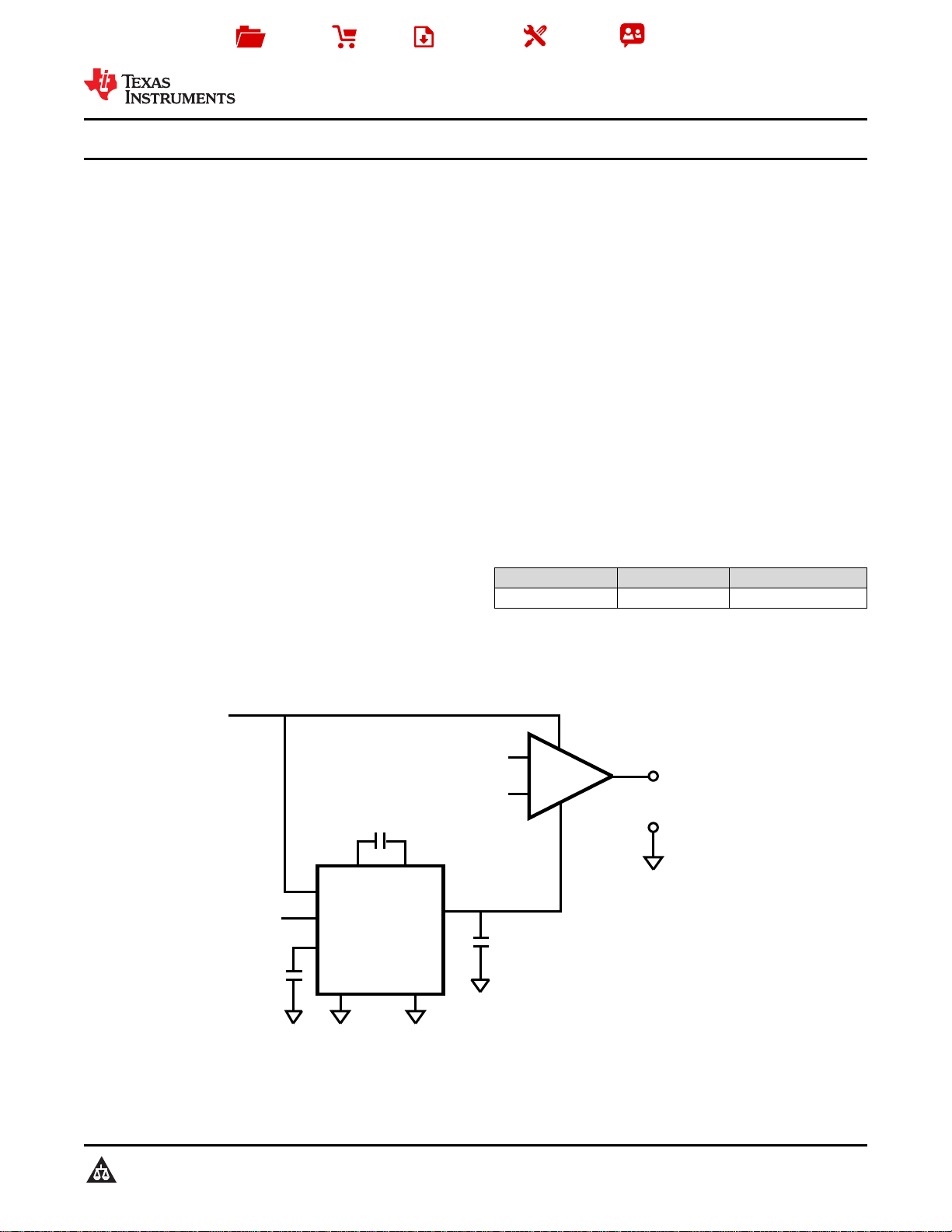
The LM7705 device is a switched capacitor voltage
inverter with a low noise, −0.23 V fixed negative
voltage regulator. This device is designed to be used
with low voltage amplifiers to enable the amplifiers
output to swing to zero volts. The −0.23 V is used to
supply the negative supply pin of an amplifier while
maintaining less then 5.5 V across the amplifier. Railto-Rail output amplifiers cannot output zero volts
when operating from a single-supply voltage and can
result in error accumulation due to amplifier output
saturation voltage being amplified by following gain
stages. A small negative supply voltage will prevent
the amplifiers output from saturating at zero volts and
will help maintain an accurate zero through a signal
processing chain. Additionally, when an amplifier is
used to drive an input of the ADC, the amplifier can
output a zero voltage signal and the full input range
of an ADC can be used. The LM7705 device has a
shutdown pin to minimize standby power
consumption.
Device Information
PART NUMBER PACKAGE BODY SIZE (NOM)
LM7705 VSSOP (8) 3.00 mm × 3.00 mm
(1) For all available packages, see the orderable addendum at
the end of the data sheet.
(1)
Typical Application
1
An IMPORTANT NOTICE at the end of this data sheet addresses availability, warranty, changes, use in safety-critical applications,
intellectual property matters and other important disclaimers. PRODUCTION DATA.
Page 2

LM7705
SNVS420D –NOVEMBER 2008–REVISED MAY 2018
www.ti.com
Table of Contents
1 Features.................................................................. 1
2 Applications ........................................................... 1
3 Description ............................................................. 1
4 Revision History..................................................... 2
5 Pin Configuration and Functions......................... 3
6 Specifications......................................................... 3
6.1 Absolute Maximum Ratings...................................... 3
6.2 ESD Ratings.............................................................. 3
6.3 Recommended Operating Conditions....................... 4
6.4 Thermal Information.................................................. 4
6.5 3.3-V Electrical Characteristics................................. 4
6.6 5-V Electrical Characteristics.................................... 5
6.7 Typical Characteristics.............................................. 6
7 Detailed Description............................................ 10
7.1 Overview................................................................. 10
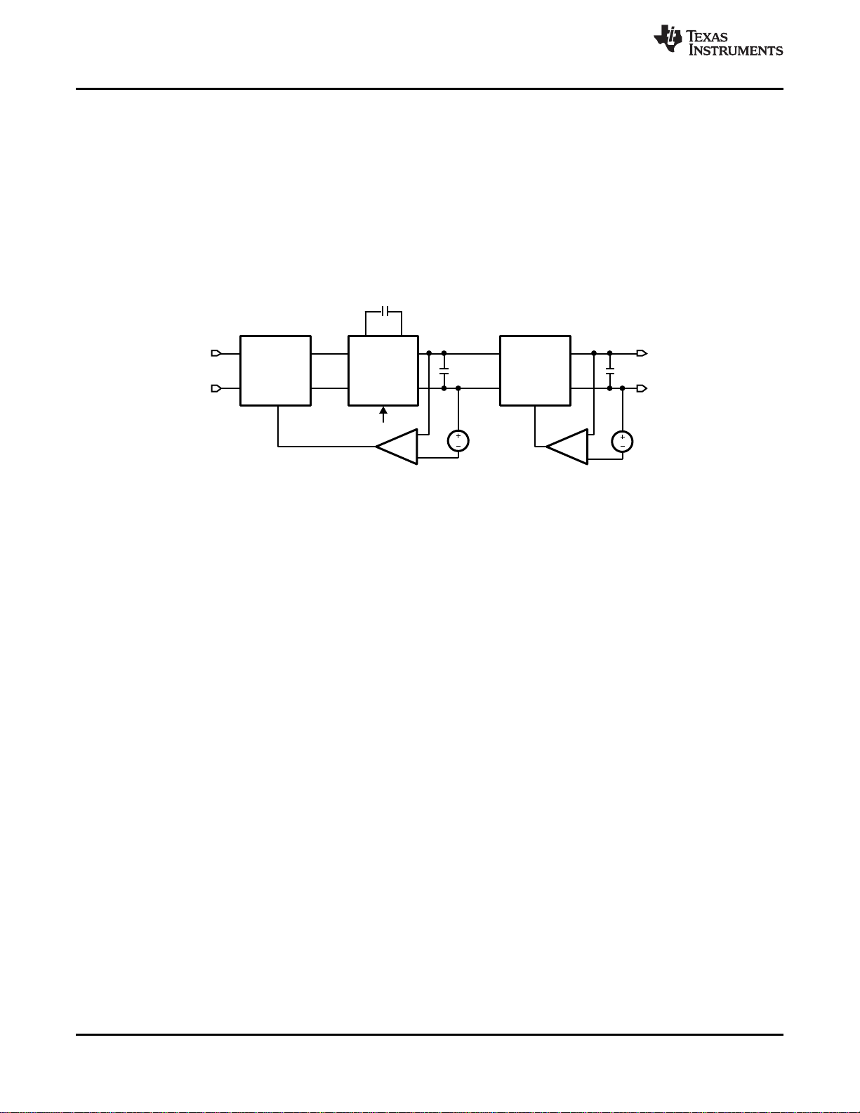
7.2 Functional Block Diagram....................................... 10
7.3 Feature Description................................................. 10
7.4 Device Functional Modes........................................ 10
8 Application and Implementation ........................ 14
8.1 Application Information............................................ 14
8.2 Typical Application.................................................. 16
9 Power Supply Recommendations...................... 18
10 Layout................................................................... 19
10.1 Layout Guidelines ................................................. 19
10.2 Layout Examples................................................... 19
11 Device and Documentation Support................. 20
11.1 Community Resources.......................................... 20
11.2 Trademarks........................................................... 20
11.3 Electrostatic Discharge Caution............................ 20
11.4 Glossary................................................................ 20
12 Mechanical, Packaging, and Orderable
Information........................................................... 20
4 Revision History
NOTE: Page numbers for previous revisions may differ from page numbers in the current version.
Changes from Revision C (September 2015) to Revision D Page
• Deleted 'Maximum Output Current 26 mA' from Features list ............................................................................................... 1
• Deleted IO_MAX spec from 3.3-V Electrical Characteristics and 5-V Electrical Characteristics tables.................................. 4
Changes from Revision B (March 2013) to Revision C Page
• Added Pin Configuration and Functions section, ESD Ratings table, Feature Description section, Device Functional
Modes, Application and Implementation section, Power Supply Recommendations section, Layout section, Device
and Documentation Support section, and Mechanical, Packaging, and Orderable Information section .............................. 1
Changes from Revision A (November 2008) to Revision B Page
• Changed layout of National Semiconductor Data Sheet to TI format .................................................................................. 19
2
Submit Documentation Feedback Copyright © 2008–2018, Texas Instruments Incorporated
Product Folder Links: LM7705
Page 3
1
4
5
8
LM7705
www.ti.com
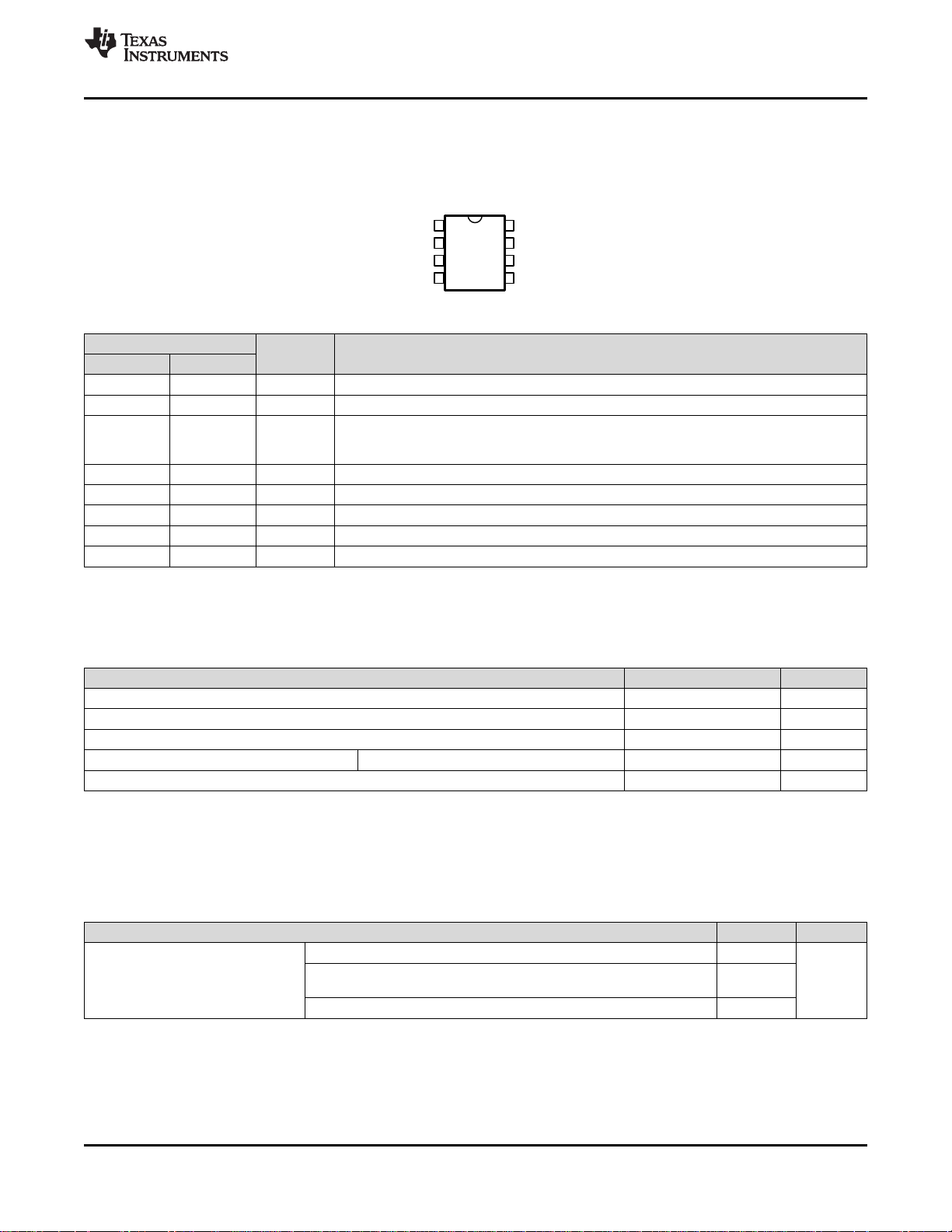
5 Pin Configuration and Functions
PIN
NAME NO.
C
F+
V
SS
1 Analog C
2 Ground Power Ground
SD 3 Input
V
DD
V
SS
V
OUT
C
RES
C
F-
4 Power Positive Supply Voltage
5 Ground Power Ground
6 Output Output Voltage
7 Analog Reserve Capacitor Connection
8 Analog C
TYPE DESCRIPTION
Positive Capacitor Connection
FLY
Shutdown Pin
If SD pin is LOW, device is ON
If SD pin is HIGH, device is OFF
Negative Capacitor Connection
FLY
LM7705
SNVS420D –NOVEMBER 2008–REVISED MAY 2018
DGK Package
8-Pin VSSOP
Top View
Pin Functions
6 Specifications
6.1 Absolute Maximum Ratings
over operating free-air temperature range (unless otherwise noted)
Supply voltage VDD- V
SD VDD+ 0.3 VSS– 0.3 V
Junction temperature
Mounting temperature Infrared or Convection (20 sec) 260 °C
Storage temperature, T
(1) Stresses beyond those listed under Absolute Maximum Ratings may cause permanent damage to the device. These are stress ratings
only, which do not imply functional operation of the device at these or any other conditions beyond those indicated under Recommended
Operating Conditions. Exposure to absolute-maximum-rated conditions for extended periods may affect device reliability.
(2) Typical values represent the most likely parametric norm as determined at the time of characterization. Actual typical values may vary
over time and will also depend on the application and configuration. The typical values are not tested and are not ensured on shipped
production material.
SS
(2)
stg
6.2 ESD Ratings
Human body model (HBM), per ANSI/ESDA/JEDEC JS-001
V
Electrostatic discharge
(ESD)
(1) Human Body Model, applicable std. MIL-STD-883, Method 3015.7.
(2) Field induced Charge-Device Model, applicable std. JESD22–C101–C. (ESD FICDM std of JEDEC).
(3) Machine model, applicable std JESD22–A115–A (ESSD MM srd of JEDEC).
Charged-device model (CDM), per JEDEC specification JESD22-
(2)
C101
Machine model
(3)
(1)
MIN MAX UNIT
5.75 V
150 °C
−65 150 °C
VALUE UNIT
(1)
±2000
±750
V
±200
Product Folder Links: LM7705
Submit Documentation FeedbackCopyright © 2008–2018, Texas Instruments Incorporated
3
Page 4
LM7705
SNVS420D –NOVEMBER 2008–REVISED MAY 2018
www.ti.com
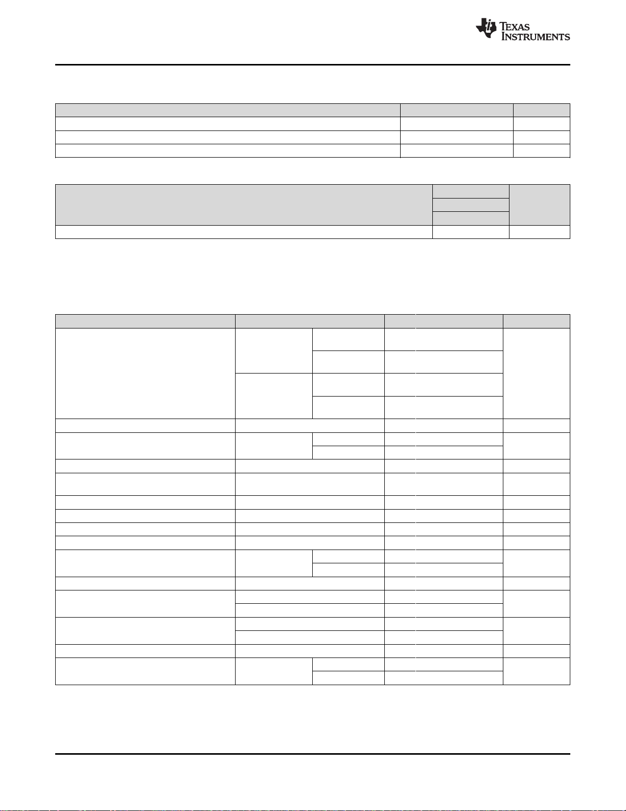
6.3 Recommended Operating Conditions
over operating free-air temperature range (unless otherwise noted)
MIN MAX UNIT
Supply voltage (VDDto GND) 3 5.25 V
Supply voltage (VDDwrt V
Temperature range −40 125 °C
) 3.23 5.48 V
OUT
6.4 Thermal Information
LM77005
THERMAL METRIC
(1)
UNITDGK (VSSOP)
8 PINS
R
θJA
Junction-to-ambient thermal resistance 253 °C/W
(1) For more information about traditional and new thermal metrics, see the Semiconductor and IC Package Thermal Metrics application
report, SPRA953.
6.5 3.3-V Electrical Characteristics
Unless otherwise specified, all limits are ensured for TA= 25°C, VDD= 3.3 V, VSS= 0 V, SD = 0 V, C
C
= 22 µF.
OUT
V
OUT
V
R
I
S
I
SD
η
POWER
η
POWER
t
ON
t
OFF
t
OFF CP
Z
OUT
f
OSC
V
IL
V
IH
I
C
PARAMETER TEST CONDITIONS MIN
TA= 25°C
I
= 0 mA
OUT
−40°C to 125°C
Output Voltage
TA= 25°C
I
= −20 mA
OUT
−40°C to 125°C
Output Voltage Ripple I
Supply Current No Load
Shutdown Supply Current SD = V
Current Conversion Efficiency
Current Conversion Efficiency I
Turnon Time I
Turnoff Time I
Turnoff Time Charge Pump I
Output Impedance
= −20 mA 4 mV
OUT
TA= 25°C 50 78 100
−40°C to 125°C 150
DD
−5 mA ≤ I
−20 mA
= −5 mA 98%
OUT
= −5 mA 500 μs
OUT
= −5 mA 700 μs
OUT
= −5 mA 11 μs
OUT
−1 mA ≤ I
−20 mA
OUT
OUT
≤
TA= 25°C 0.23 0.8
≤
−40°C to 125°C 1.3
Oscillator Frequency 92 kHz
Shutdown Input Low
Shutdown Input High
Shutdown Pin Input Current SD = V
Load Regulation
TA= 25°C 1.6
−40°C to 125°C 1.25
TA= 25°C 1.85
−40°C to 125°C 2.15
DD
0 mA ≤ I
−20 mA
OUT
≤
TA= 25°C 0.12 0.6
−40°C to 125°C 0.85
(1)
−0.24
−0.25
−0.24
−0.25
TYP
−0.232 −0.219
2
1
−0.226 −0.219
2
1
(2)
98%
= 5 µF, C
FLY
MAX
(1)
RES
= 22 µF,
UNIT
−0.209
−0.209
μA
20 nA
50 pA
%/mA
V
PP
Ω
V
V
(1) All limits are specified by testing or statistical analysis.
(2) Typical values represent the most likely parametric norm as determined at the time of characterization. Actual typical values may vary
over time and will also depend on the application and configuration. The typical values are not tested and are not specified on shipped
production material.
4
Submit Documentation Feedback Copyright © 2008–2018, Texas Instruments Incorporated
Product Folder Links: LM7705
Page 5
www.ti.com
3.3-V Electrical Characteristics (continued)
LM7705
SNVS420D –NOVEMBER 2008–REVISED MAY 2018
Unless otherwise specified, all limits are ensured for TA= 25°C, VDD= 3.3 V, VSS= 0 V, SD = 0 V, C
C
= 22 µF.
OUT
PARAMETER TEST CONDITIONS MIN
Line Regulation
3 V ≤ VDD≤ 5.25 V
(No Load)
TA= 25°C –0.2 0.29 0.7
−40°C to 125°C 1.1
(1)
TYP
(2)
= 5 µF, C
FLY
MAX
= 22 µF,
RES
(1)
UNIT
%/V
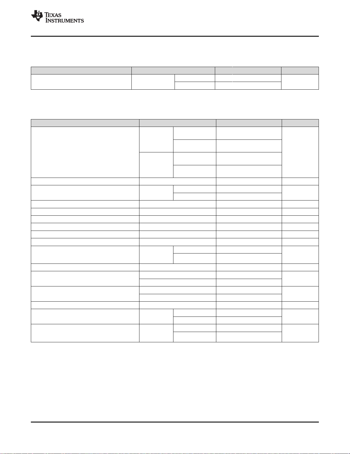
6.6 5-V Electrical Characteristics
Unless otherwise specified, all limits are ensured for TA= 25°C, VDD= 5.0V, VSS= 0V, SD = 0V, C
C
= 22 µF.
OUT
PARAMETER TEST CONDITIONS MIN
TA= 25°C
I
= 0 mA
OUT
−40°C to 125°C
V
OUT
Output Voltage
TA= 25°C
I
= −20 mA
OUT
−40°C to 125°C
V
R
I
S
I
SD
η
POWER
η
POWER
t
ON
t
OFF
t
OFF CP
Z
OUT
f
OSC
V
IL
V
IH
I
C
Output Voltage Ripple I
Supply Current No Load
Shutdown Supply Current SD = V
Current Conversion Efficiency −5 mA ≤ I
Current Conversion Efficiency I
Turnon Time I
Turnoff Time I
Turnoff Time Charge Pump I
Output Impedance
= −20 mA 4 mV
OUT
TA= 25°C 60 103 135
−40°C to 125°C 240
DD
≤ −20 mA 98%
OUT
= −5 mA 98%
OUT
= −5 mA 200 μs
OUT
= −5 mA 700 μs
OUT
= −5 mA 11 μs
OUT
−1 mA ≤ I
≤
−20 mA
TA= 25°C 0.26 0.8
OUT
−40°C to 125°C 1.3
Oscillator Frequency 91 kHz
Shutdown Input Low
Shutdown Input High
Shutdown Pin Input Current SD = V
Load Regulation
Line Regulation
TA= 25°C 2.55
−40°C to 125°C 1.95
TA= 25°C 2.8
−40°C to 125°C 3.25
DD
0 mA ≤ I
−20 mA
3 V ≤ V
DD
5.25 V (No
Load)
TA= 25°C 0.14 0.6
≤
OUT
−40°C to 125°C 0.85
≤
TA= 25°C −0.2 0.29 0.7
−40°C to 125°C 1.1
(1) All limits are specified by testing or statistical analysis.
(2) Typical values represent the most likely parametric norm as determined at the time of characterization. Actual typical values may vary
over time and will also depend on the application and configuration. The typical values are not tested and are not specified on shipped
production material.
−0.24
−0.25
−0.24
−0.25
(1)
TYP
−0.233 −0.219
2
1
−0.226 −0.219
2
1
FLY
(2)
= 5 µF, C
(1)
MAX
RES
= 22 µF,
UNIT
−0.209
−0.209
μA
20 nA
50 pA
%/mA
%/V
V
PP
Ω
V
V
Product Folder Links: LM7705
Submit Documentation FeedbackCopyright © 2008–2018, Texas Instruments Incorporated
5
Page 6
TEMPERATURE (°C)
OUTPUT VOLTAGE RIPPLE
(mV
PP
)
15
12
9
6
3
0
-40 0 40 80 120
C
RES
= C
FILTER
= 22 éF
C
RES
= C
FILTE
R
= 10 éF
SUPPLY VOLTAGE = 3.3V
TEMPERATURE (°C)
OUTPUT VOLTAGE RIPPLE
(mV
PP
)
15
12
9
6
3
0
-40 0 40 80 120
C
RES
= C
FILTER
= 22 éF
C
RES
= C
FILTER
= 10 éF
SUPPLY VOLTAGE = 5.0V
OUTPUT CURRENT (mA)
OUTPUT VOLTAGE (V)
-0.20
-0.21
-0.22
-0.23
-0.24
-0.25
0 5 10 15 20 25 30
-40°C
125°C
25°C
85°C
SUPPLY VOLTAGE = 3.3V
OUTPUT CURRENT (mA)
OUTPUT VOLTAGE (V)
-0.20
-0.21
-0.22
-0.23
-0.24
-0.25
0 10 20 30 40 50 60
-40°C
125°C
25°C
85°C
SUPPLY VOLTAGE = 5.0V
SUPPLY VOLTAGE (V)
OUTPUT VOLTAGE (V)
-0.19
-0.20
-0.21
-0.22
-0.23
-0.24
3.0 3.5 4.0 4.5 5.0
I
OUT
= 0 mA
I
OUT
= 5 mA
I
OUT
=10 mA
I
OUT
= 20 mA
SUPPLY VOLTAGE (V)
SUPPLY CURRENT (éA)
300
250
200
150
100
50
0
3.0 3.5 4.0 4.5 5.0
-40°C
125°C
25°C
85°C
LM7705
SNVS420D –NOVEMBER 2008–REVISED MAY 2018
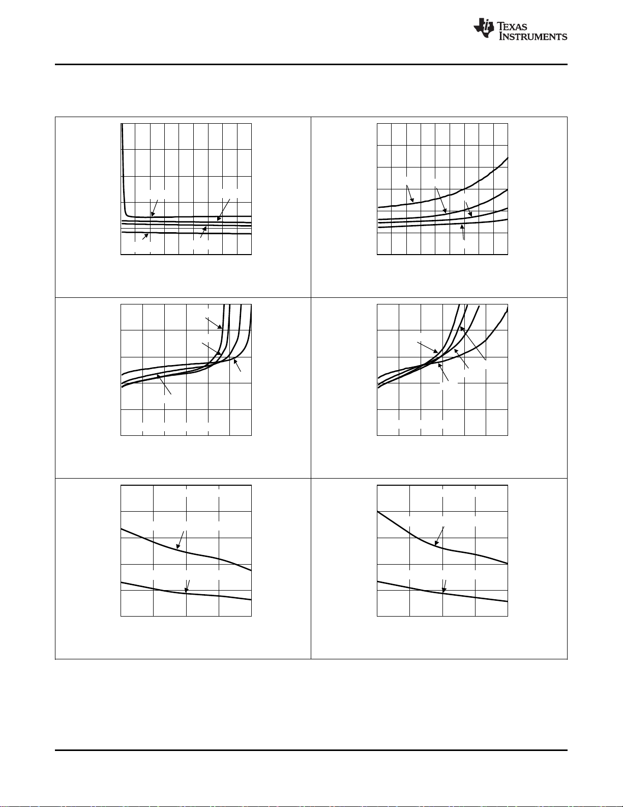
6.7 Typical Characteristics
VDD= 3.3 V and TA= 25°C unless otherwise noted.
Figure 1. Output Voltage vs. Supply Voltage Figure 2. Supply Current vs. Supply Voltage
www.ti.com
Figure 3. Output Voltage vs. Output Current Figure 4. Output Voltage vs. Output Current
6
Figure 5. Output Voltage Ripple vs. Temperature Figure 6. Output Voltage Ripple vs. Temperature
Submit Documentation Feedback Copyright © 2008–2018, Texas Instruments Incorporated
Product Folder Links: LM7705
Page 7
ENABLE VOLTAGE
TURN ON TIME (200 és/DIV)
OUTPUT VOLTAGE (0.2V/DIV)
ENABLE PULSE
0 mA
5 mA
10 mA
20 mA
SUPPLY VOLTAGE = 3.3V
0V
0V
ENABLE VOLTAGE
TURN ON TIME (100 és/DIV)
OUTPUT VOLTAGE (0.2V/DIV)
ENABLE PULSE
0 mA
5 mA
10 mA
20 mA
0V
0V
SUPPLY VOLTAGE = 5.0V
OUTPUT CURRENT (mA)
CURRENT CONVERSION EFFICIECY (%)
110
105
100
95
90
85
80
0 4 8 12 16 20
-40°C
125°C
25°C
85°C
SUPPLY VOLTAGE = 3.3V
OUTPUT CURRENT (mA)
CURRENT CONVERSION EFFICIECY (%)
110
105
100
95
90
85
80
0 4 8 12 16 20
-40°C
125°C
25°C
85°C
SUPPLY VOLTAGE = 5.0V
OUTPUT CURRENT (mA)
SUPPLY CURRENT
(mA)
20
16
12
8
4
0
0 4 8 12 16 20
-40°C
125°C
25°C
85°C
SUPPLY VOLTAGE = 3.3V
OUTPUT CURRENT (mA)
SUPPLY CURRENT
(mA)
20
16
12
8
4
0
0 4 8 12 16 20
-40°C
125°C
25°C
85°C
SUPPLY VOLTAGE = 5.0V
www.ti.com
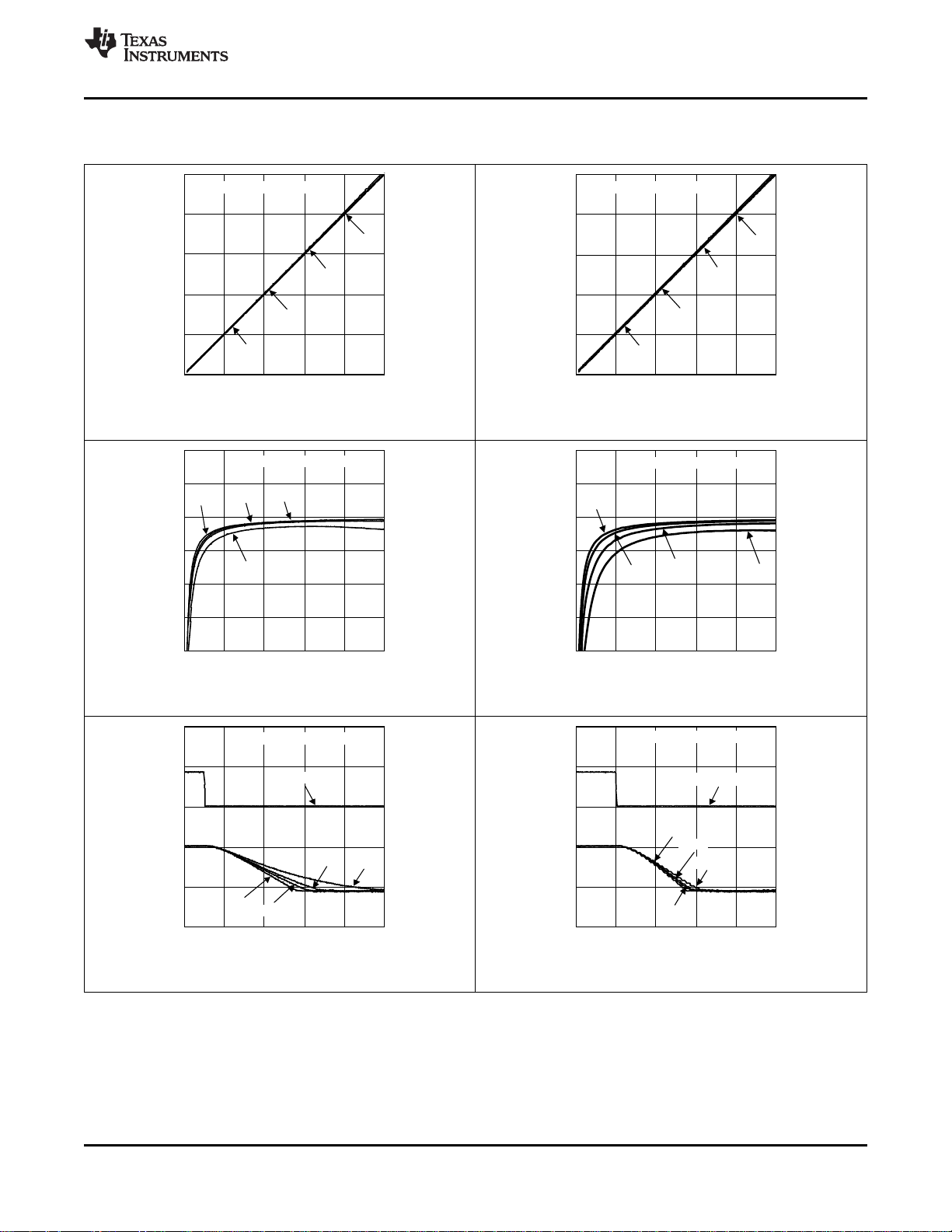
Typical Characteristics (continued)
VDD= 3.3 V and TA= 25°C unless otherwise noted.
Figure 7. Supply Current vs. Output Current Figure 8. Supply Current vs. Output Current
LM7705
SNVS420D –NOVEMBER 2008–REVISED MAY 2018
Figure 9. Current Conversion Efficiency vs. Output Current Figure 10. Current Conversion Efficiency vs. Output Current
Figure 11. Turnon Time Figure 12. Turnon Time
Submit Documentation FeedbackCopyright © 2008–2018, Texas Instruments Incorporated
Product Folder Links: LM7705
7
Page 8
OUTPUT CURRENT (mA)
TIME (20 us/DIV)
OUTPUT VOLTAGE (V)
-0.210
-0.218
-0.226
-0.234
-0.242
-0.250
40
30
20
10
0
-10
OUTPUT CURRENT
+25°C
+85/+125°C
-40°C
SUPPLY VOLTAGE = 3.3V
OUTPUT CURRENT (mA)
TIME (20 us/DIV)
OUTPUT VOLTAGE (V)
-0.210
-0.218
-0.226
-0.234
-0.242
-0.250
40
30
20
10
0
-10
OUTPUT CURRENT
+25°C
+85/+125°C
-40°C
SUPPLY VOLTAGE = 5V
OUTPUT CURRENT (mA)
TIME (20 us/DIV)
OUTPUT VOLTAGE (V)
-0.210
-0.218
-0.226
-0.234
-0.242
-0.250
40
30
20
10
0
-10
OUTPUT CURRENT
+25°C
+85/+125°C
-40°C
SUPPLY VOLTAGE = 3.3V
OUTPUT CURRENT (mA)
TIME (20 us/DIV)
OUTPUT VOLTAGE (V)
-0.210
-0.218
-0.226
-0.234
-0.242
-0.250
40
30
20
10
0
-10
OUTPUT CURRENT
+25°C
+85/+125°C
-40°C
SUPPLY VOLTAGE = 5V
TEMPERATURE (°C)
LOAD REGULATION (%/mA)
0.4
0.3
0.2
0.1
0.0
-40 0 40 80 120
SUPPLY VOLTAGE = 3.3V
TEMPERATURE (°C)
LOAD REGULATION (%/mA)
0.4
0.3
0.2
0.1
0.0
-40 0 40 80 120
SUPPLY VOLTAGE = 5.0V
LM7705
SNVS420D –NOVEMBER 2008–REVISED MAY 2018
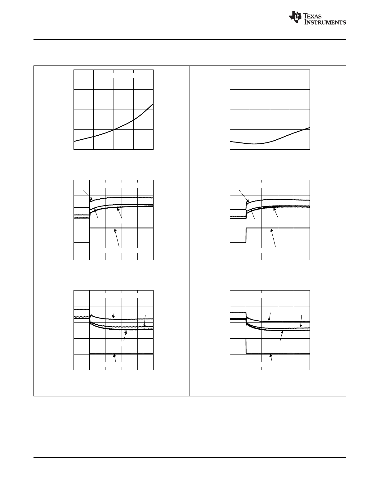
Typical Characteristics (continued)
VDD= 3.3 V and TA= 25°C unless otherwise noted.
Figure 13. Load Regulation vs. Temperature Figure 14. Load Regulation vs. Temperature
www.ti.com
8
Submit Documentation Feedback Copyright © 2008–2018, Texas Instruments Incorporated
Figure 15. Transient Response Figure 16. Transient Response
Figure 17. Transient Response Figure 18. Transient Response
Product Folder Links: LM7705
Page 9
TEMPERATURE (°C)
OSCILLATOR FREQUENCY (kHz)
100
95
90
85
80
75
70
-40 0 40 80 120
SUPPLY VOLTAGE = 3.3V
SUPPLY VOLTAGE = 5V
SHUTDOWN VOLTAGE (V)
OUTPUT VOLTAGE (V)
0
-0.05
-0.10
-0.15
-0.20
-0.25
0 1 2 3 4 5
SUPPLY
VOLTAGE = 5V
SUPPLY
VOLTAGE = 3.3V
SHUTDOWN VOLTAGE (V)
SUPPLY CURRENT (éA)
300
250
200
150
100
50
0
0 1 2 3 4 5
SUPPLY VOLTAGE = 5V
SUPPLY VOLTAGE = 3.3V
www.ti.com
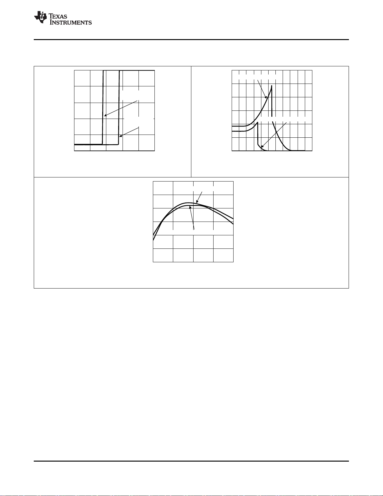
Typical Characteristics (continued)
VDD= 3.3 V and TA= 25°C unless otherwise noted.
Figure 19. Output voltage vs. Shutdown Voltage Figure 20. Supply Current vs. Shutdown Voltage
LM7705
SNVS420D –NOVEMBER 2008–REVISED MAY 2018
Figure 21. Oscillator Frequency vs. Temperature
Product Folder Links: LM7705
Submit Documentation FeedbackCopyright © 2008–2018, Texas Instruments Incorporated
9
Page 10
C
FLY
CHARGE
PUMP
INVERTOR
C
RESERVE
V
REF1
PRE
REGULATOR
V
CP,IN
f
osc
V
OUT
V
CP,OUT
POST
REGULATOR
C
out
V
DD
V
SS
V
SS
V
REF2
LM7705
SNVS420D –NOVEMBER 2008–REVISED MAY 2018
www.ti.com
7 Detailed Description
7.1 Overview
The LM7705 is a switched capacitor voltage inverter with a low-noise, −0.23-V fixed negative bias output. The
part will operate over a supply voltage range of 3 V to 5.25 V. Applying a logical low level to the SD input will
activate the part, and generate a fixed −0.23-V output voltage. The part can be disabled; the output is switched
to ground level, by applying a logical high level to the SD input of the part.
7.2 Functional Block Diagram
7.3 Feature Description
7.3.1 Supply Voltage
The LM7705 will operate over a supply voltage range of 3 V to 5.25 V, and meet the specifications given in the
3.3-V Electrical Characteristics Table. Supply voltage lower than 3.3 V will decrease performance (The output
voltage will shift towards zero, and the current sink capabilities will decrease) A voltage higher than 5.25 V will
exceed the Absolute Maximum Ratings ratings and therefore damage the part.
7.3.2 Output Voltage and Line Regulation
The fixed and regulated output voltage of −0.23 V has tight limits, as indicated in the 3.3-V Electrical
Characteristics table, to ensure a stable voltage level. The usage of the pre- and post regulator in combination
with the charge pump inverter ensures good line regulation of 0.29%/V
7.3.3 Output Current and Load Regulation
The LM7705 can sink currents more than 26 mA, causing an output voltage shift to −200 mV. A specified loadregulation of 0.14% mA/V ensures a minor voltage deviation for load current up to 20 mA.
7.3.4 Quiescent Current
The LM7705 consumes a quiescent current less than 100 µA. Sinking a load current, will result in a current
conversion efficiency better than 90%, even for load currents of 1 mA, increasing to 98% for a current of 5mA.
7.4 Device Functional Modes
7.4.1 General Amplifier Application
This section will discuss a general DC coupled amplifier application. First, one of the limitations of a DC coupled
amplifier is discussed. This is illustrated with two application examples. A solution is a given for solving this
limitation by using the LM7705.
Due to the architecture of the output stage of general amplifiers, the output transistors will saturate. As a result,
the output of a general purpose op amp can only swing to a few 100 mV of the supply rails. Amplifiers using
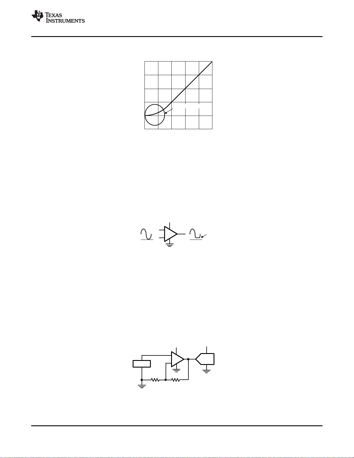
CMOS technology do have a lower output saturation voltage. This is illustrated in Figure 22. For example, Texas
Instruments' LM7332 can swing to 200 mV to the negative rail, for a 10-kΩ load, over all temperatures.
10
Submit Documentation Feedback Copyright © 2008–2018, Texas Instruments Incorporated
Product Folder Links: LM7705
Page 11
+V
ADC
R
F1
-
+
V
REF
R
G1
GAIN = 50x
ADC122S021LMP7701
SENSOR
V
IN
+V
-
+
0V
V
OUT
0V
V
DSAT
INPUT VOLTAGE (V)
OUTPUT VOLTAGE (V)
V+
0
0 V+
V
DSAT
OUTPUT SATURATION
LM7705
www.ti.com
SNVS420D –NOVEMBER 2008–REVISED MAY 2018
Device Functional Modes (continued)
Figure 22. Limitation of the Output of an Amplifier
The introduction of operational amplifiers with output rail-to-rail drive capabilities is a strong improvement and the
(output) performance of op amps is for many applications no longer a limiting factor. For example, Texas
Instruments' LMP7701 (a typical rail-to-rail op amp), has an output drive capability of only 50 mV over all
temperatures for a 10-kΩ load resistance. This is close to the lower supply voltage rail.
However, for true zero output applications with a single supply, the saturation voltage of the output stage is still a
limiting factor. This limitation has a negative impact on the functionality of true zero output applications. This is
illustrated in Figure 23.
In the One-Stage, Single-Supply True Zero Amplifier section, two applications will be discussed, showing the
limitations of the output stage of an op amp in a single supply configuration:
• A single stage true zero amplifier, with a 12-bit ADC back end.
• A dual stage true zero amplifier, with a 12-bit ADC back end.
7.4.1.1 One-Stage, Single-Supply True Zero Amplifier
This application shows a sensor with a DC output signal, amplified by a single supply op amp. The output voltage
of the op amp is converted to the digital domain using an Analog to Digital Converter (ADC). Figure 24 shows the
basic set-up of this application.
Figure 23. Output Limitation for Single-Supply True Zero Output Application
Figure 24. Sensor With DC Output and a Single-Supply Op Amp
Product Folder Links: LM7705
Submit Documentation FeedbackCopyright © 2008–2018, Texas Instruments Incorporated
11
Page 12
+V
R
F1
-
+
R
G1
R
F2
-
+
R
G2
A
1
A
2
ADC
V
REF
+V
GAIN = 10x
GAIN = 5x
ADC122S021
1/2 LMP7702
1/2 LMP7702
SENSOR
LM7705
SNVS420D –NOVEMBER 2008–REVISED MAY 2018
www.ti.com
Device Functional Modes (continued)
The sensor has a DC output signal that is amplified by the op amp. For an optimal signal-to-noise ratio, the
output voltage swing of the op amp must be matched to the input voltage range of the Analog to Digital
Converter (ADC). For the high side of the range this can be done by adjusting the gain of the op amp. However,
the low side of the range cannot be adjusted and is affected by the output swing of the op amp.
Example:
Assume the output voltage range of the sensor is 0 to 90 mV. The available op amp is a LMP7701, using a 0/+5V supply voltage, having an output drive of 50 mV from both rails. This results in an output range of 50 mV to
4.95V.
Select two resistors values for RG1and RF1that result in a gain of 50x. The output of the LMP7701 must swing
from 0 mV to 4.5 V. The higher value is no problem, however the lower swing is limited by the output of the
LM7701 and won’t go below 50 mV instead of the desired 0 V, causing a non-linearity in the sensor reading.
When using a 12-bit ADC, and a reference voltage of 5 V (having an ADC step size of approximate 1.2 mV), the
output saturation results in a loss of the lower 40 quantization levels of the ADCs dynamic range.
7.4.1.2 Two-Stage, Single-Supply True Zero Amplifier
This sensor application produces a DC signal, amplified by a two cascaded op amps, having a single supply. The
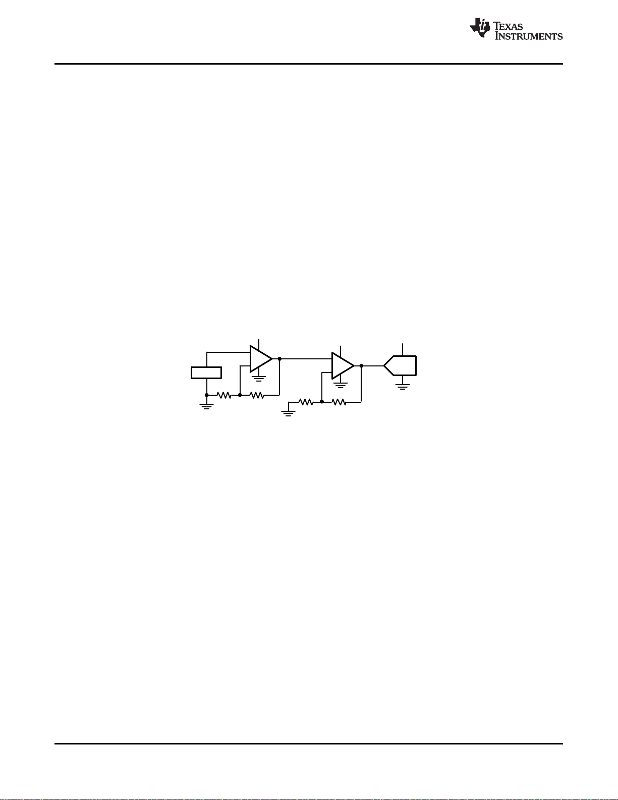
output voltage of the second op amp is converted to the digital domain. Figure 25 shows the basic setup of this
application.
Figure 25. Sensor With DC Output and a 2-Stage, Single-Supply Op Amp
The sensor generates a DC output signal. In this case, a DC coupled, 2-stage amplifier is used. The output
voltage swing of the second op amp must me matched to the input voltage range of the Analog to Digital
Converter (ADC). For the high side of the range this can be done by adjusting the gain of the op amp. However,
the low side of the range can’t be adjusted and is affected by the output drive of the op amp.
Example:
Assume; the output voltage range of the sensor is 0 to 90 mV. The available op amp is a LMP7702 (Dual
LMP7701 op amp) that can be used for A1and A2. The op amp is using a 0/+5-V supply voltage, having an
output drive of 50 mV from both rails. This results in an output range of 50 mV to 4.95 V for each individual
amplifier.
Select two resistors values for RG1and RF1that result in a gain of 10x for the first stage (A1) and a gain of 5x for
the second stage (A2) The output of the A2in the LMP7702 must swing from 0V to 4.5 V. This swing is limited by
the 2 different factors:
1. The high voltage swing is no problem; however the low voltage swing is limited by the output saturation
voltage of A2from the LM7702 and will not go below 50 mV instead of the desired 0 V.
2. Another effect has more impact. The output saturation voltage of the first stage will cause an offset for the
input of the second stage. This offset of A1is amplified by the gain of the second stage (10x in this example),
resulting in an output offset voltage of 500mV. This is significantly more that the 50 mV (V
DSAT
) of A2.
When using a 12-bit ADC, and a reference voltage of 5 Volt (having an ADC step size of approximate 1.2 mV),
the output saturation results in a loss of the lower 400 quantization levels of the ADCs dynamic range. This will
cause a major non-linearity in the sensor reading.
12
Submit Documentation Feedback Copyright © 2008–2018, Texas Instruments Incorporated
Product Folder Links: LM7705
Page 13
V
IN
+V
-
+
0V
V
OUT
0V
-V
LM7705
www.ti.com
SNVS420D –NOVEMBER 2008–REVISED MAY 2018
Device Functional Modes (continued)
7.4.1.3 Dual-Supply, True Zero Amplifiers
The limitations of the output stage of the op amp, as indicated in both examples, can be omitted by using a dual
supply op amp. The output stage of the used op amp can then still swing from 50 mV of the supply rails.
However, the functional output range of the op amp is now from ground level to a value near the positive supply
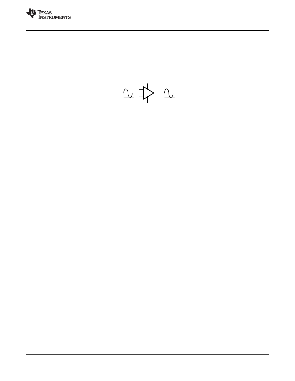
rail. Figure 26 shows the output drive of an amplifier in a true zero output voltage application.
Figure 26. Amplifier Output Drive With a Dual-Supply
Disadvantages of this solution are:
• The usage of a dual-supply instead of a simple single supply is more expensive.
• A dual supply voltage for the op amps requires parts that can handle a larger operating range for the supply
voltage. If the op amps used in the current solution cannot handle this, a redesign can be required.
A better solution is to use the LM7705. This low-noise negative bias generator has some major advantages with
respect to a dual-supply solution:
• Operates with only a single positive supply, and is therefore a much cheaper solution.
• The LM7705 generates a negative supply voltage of only −0.23 V. This is more than enough to create a Truezero output for most op amps.
• In many applications, this small extension of the supply voltage range can be within the abs max rating for
many op amps, so an expensive redesign is not necessary.
In the Typical Application section, a typical amplifier application will be evaluated. The performance of an
amplifier will be measured in a single supply configuration. The results will be compared with an amplifier using a
LM7705 supplying a negative voltage to the bias pin.
Product Folder Links: LM7705
Submit Documentation FeedbackCopyright © 2008–2018, Texas Instruments Incorporated
13
Page 14
POWER
SUPPLY
PRE
REGULATOR
LOAD
CHARGE
PUMP
POST
REGULATOR
LM7705
V
+
OSCILLATOR
C
FLY
OUT=V-
C
RES
CAP
+
CAP
-
S2
S1
S4
S3
Ó1
Ó2
LM7705
SNVS420D –NOVEMBER 2008–REVISED MAY 2018
www.ti.com
8 Application and Implementation
NOTE
Information in the following applications sections is not part of the TI component
specification, and TI does not warrant its accuracy or completeness. TI’s customers are
responsible for determining suitability of components for their purposes. Customers should
validate and test their design implementation to confirm system functionality.
8.1 Application Information
8.1.1 Functional Description
The LM7705, low-noise negative bias generator, can be used for many applications requiring a fixed negative
voltage. A key application for the LM7705 is an amplifier with a true zero output voltage using the original parts,
while not exceeding the maximum supply voltage ratings of the amplifier.
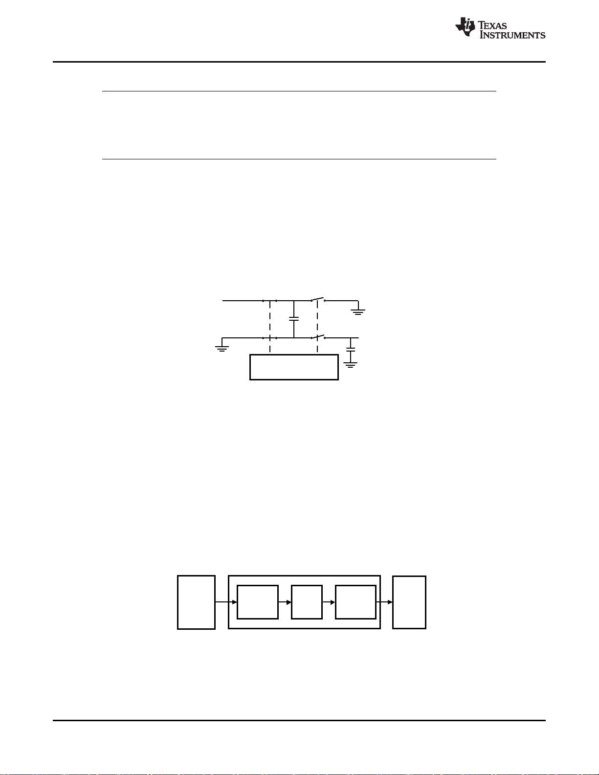
The voltage inversion in the LM7705 is achieved using a switched capacitor technique with two external
capacitors (C
storage capacitors. This switched capacitor technique is given in Figure 27.
FLY
and C
). An internal oscillator and a switching network transfers charge between the two
RES
Figure 27. Voltage Inverter
The internal oscillator generates two anti-phase clock signals. Clock 1 controls switches S1 and S2. Clock 2
controls switches S3 and S4. When Switches S1 and S2 are closed, capacitor C
switches S3 and S4 are closed (S1 and S2 are open) charge from C
is transferred to C
FLY
is charged to V+. When
FLY
and the output
RES
voltage OUT is equal to –V+.
Due to the switched capacitor technique, a small ripple will be present at the output voltage with a frequency of
the oscillator. The magnitude of this ripple will increase for increasing output currents. The magnitude of the
ripple can be influenced by changing the values of the used capacitors.
8.1.2 Technical Description
As indicated in Functional Description, the main function of the LM7705 is to supply a stabilized negative bias
voltage to a load, using only a positive supply voltage. A general block diagram for this charge pump inverter is
given in Figure 28. The external power supply and load are added in this diagram as well.
Figure 28. LM7705 Architecture
The architecture given in Figure 28 shows that the LM7705 contains 3 functional blocks:
• Pre-regulator
• Charge pump inverter
• Post-regulator
14
Submit Documentation Feedback Copyright © 2008–2018, Texas Instruments Incorporated
Product Folder Links: LM7705
Page 15
I = f Âq = f C
FLY
(V1 ± V2)
Âq = q1 -q2 = C
FLY
(V1 ± V2)
V
1
V
2
C
RES
R
L
C
FLY
BA
C
FLY
CHARGE
PUMP
INVERTOR
C
RESERVE
V
REF1
PRE
REGULATOR
V
CP,IN
f
osc
V
OUT
V
CP,OUT
POST
REGULATOR
C
out
V
DD
V
SS
V
SS
V
REF2
LM7705
www.ti.com
SNVS420D –NOVEMBER 2008–REVISED MAY 2018
Application Information (continued)
The output voltage is stabilized by:
• Controlling the power supplied from the power supply to the charge pump input by the pre-regulator
• The power supplied from the charge pump output to the load by the post-regulator.
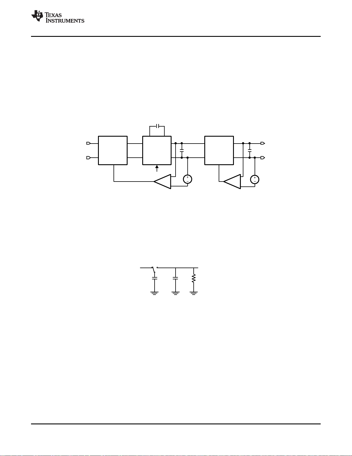
A more detailed block diagram of the negative bias generator is given in Figure 29. The control of the preregulator is based on measuring the output voltage of the charge pump. The goal of the post-regulator is to
provide an accurate controlled negative voltage at the output, and acts as a lowpass filter to attenuate the output
voltage ripple. The voltage ripple is a result of the switching behavior of the charge pump and is dependent of the
output current and the values of the used capacitors.
Figure 29. Charge Pump Inverter With Input and Output Control
In Charge Pump Theory, a simple equation will be derived that shows the relation between the ripple of the
output current, the frequency of the internal clock generator and the value of the capacitor placed at the output of
the LM7705.
8.1.3 Charge Pump Theory
This section uses a simplified but realistic equivalent circuit that represents the basic function of the charge
pump. The schematic is given in Figure 30.
Figure 30. Charge Pump
When the switch is in position A, capacitor C
Q1= C
charge on C
× V1. The switch then moves to position B, discharging C
FLY
will be Q2= C
FLY
× V2. The charge has been transferred from the source V1to the output V2. The
FLY
will charge to voltage V1. The total charge on capacitor C
FLY
to voltage V2. After this discharge, the
FLY
FLY
amount of charge transferred is:
(1)
When the switch changes between A and B at a frequency f, the charge transfer per unit time, or current is:
is
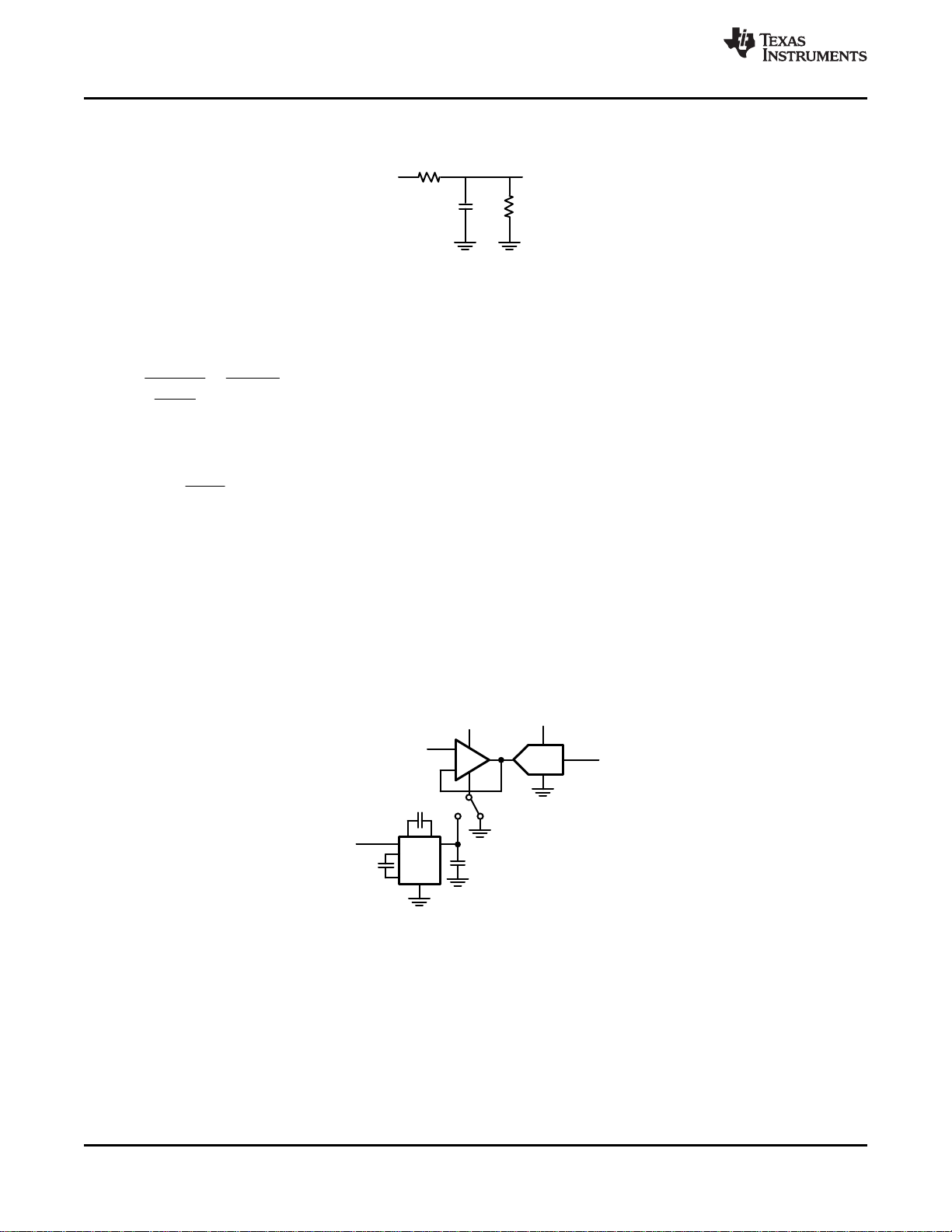
The switched capacitor network can be replaced by an equivalent resistor, as indicated in Figure 31.
Product Folder Links: LM7705
(2)
Submit Documentation FeedbackCopyright © 2008–2018, Texas Instruments Incorporated
15
Page 16
V
IN
+V
ADC
-
+
V
REF
LMP7701 ADC122S021
SDO
LM7705
+V
C
OUT
C
RES
C
FLY
B
A
-V
REQ =
1
f C
FLY
¹
·
©
§
I =
R
EQ
1
f C
FLY
¹
·
©
§
V1 ± V2
V1 ± V2
=
V
1
V
2
R
L
R
EQ
C
RES
LM7705
SNVS420D –NOVEMBER 2008–REVISED MAY 2018
www.ti.com
Application Information (continued)
Figure 31. Switched Capacitor Equivalent Circuit
The value of this resistor is dependent on both the capacitor value and the switching frequency as given in
Equation 3
(3)
The value for REQcan be calculated from Equation 3 and is given in Equation 4
(4)
Equation 4 show that the value for the resistance at an increased internal switching frequency, allows a lower
value for the used capacitor.
8.2 Typical Application
This section shows the measurement results of a true zero output amplifier application with an analog to digital
converter (ADC) used as back-end. The biasing of the op amp can be done in two ways:
• A single supply configuration
• A single supply in combination with the LM7705, extending the negative supply from ground level to a fixed
–0.23 Voltage.
Figure 32. Typical True Zero Output Voltage Application With or Without LM7705
16
Submit Documentation Feedback Copyright © 2008–2018, Texas Instruments Incorporated
Product Folder Links: LM7705
Page 17
www.ti.com
Typical Application (continued)
8.2.1 Design Requirements
The key specifications of the used components are shown in Table 1.
Table 1. Design Parameters
PARAMETERS EXAMPLE VALUE
SUPPLY VOLTAGE/REFERENCE VOLTAGE
Supply voltage 5 V
ADC Voltage Reference 5 V
LMP7701
V
(typical) 18 mV
DSAT
V
(over temperature) 50 mV
DSAT
LM7705
Output voltage ripple 4 mV
Output voltage noise 10 mV
ADC
Type ADC122S021
Resolution 12-bit
Quantization level 5V/4096 = 1.2 mV
LM7705
SNVS420D –NOVEMBER 2008–REVISED MAY 2018
PP
PP
8.2.2 Detailed Design Procedure
8.2.2.1 Basic Setup
The basic setup of this true zero output amplifier is given in Figure 32. The LMP7701 op amp is configured as a
voltage follower to demonstrate the output limitation, due to the saturation of the output stage. The negative
power supply pin of the op amp can be connected to ground level or to the output of the negative bias generator,
to demonstrate the V
effect at the output voltage range.
DSAT
The output voltage of the LMP7701 is converted to the digital domain using an ADC122S021. This is an 12-bit
analog to digital converter with a serial data output. Data processing and graphical displaying is done with a
computer. The negative power supply pin of the op amp can be connected to ground level or to the output of the
negative bias generator, to demonstrate the effect at the output voltage range of the op amp.
Product Folder Links: LM7705
Submit Documentation FeedbackCopyright © 2008–2018, Texas Instruments Incorporated
17
Page 18
TIME (SAMPLES)
DIGITIZED OUTPUT VOLTAGE
(`V)
0.050
0.040
0.030
0.020
0.010
0.000
0 80 160 240 320 400
V
DSAT
TIME (SAMPLES)
DIGITIZED OUTPUT VOLTAGE
(V)
0.050
0.040
0.030
0.020
0.010
0.000
0 80 160 240 320 400
LM7705
SNVS420D –NOVEMBER 2008–REVISED MAY 2018
www.ti.com
8.2.3 Application Curves
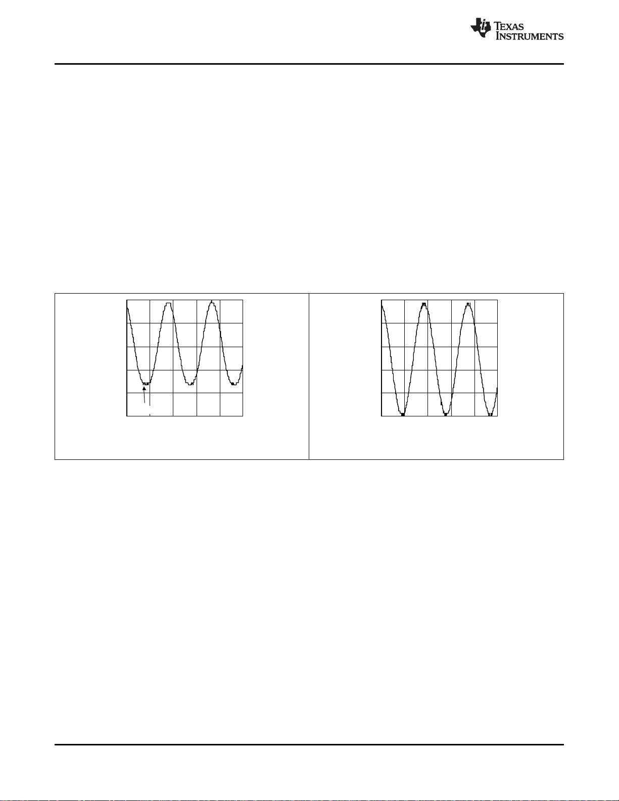
The output voltage range of the LMP7701 has been measured, especially the range to ground level. A small DC
signal, with a voltage swing of 50 mVPPis applied to the input. The digitized output voltage of the op amp is
measured over a given time period, when its negative supply pin is connected to ground level or connected to
the output of the LM7705.
Figure 33 shows the digitized output voltage of the op amp when its negative supply pin is connected to ground
level. The output of the amplifier saturates at a level of 14 mv (this is in line with the typical value of 18 mV given
in the datasheet) The graph shows some fluctuations (1-bit quantization error). Figure 34 show the digitized
output voltage of the op amp when its negative supply pin is connected to the output of the LM7705. Again, the
graph shows some 1-bit quantization errors caused by the voltage ripple and output noise. In this case the op
amps output level can reach the true zero output level.
Figure 33 and Figure 34 show that:
• With a single supply, the output of the amplifier is limited by the V
of the output stage.
DSAT
• The amplifier can be used as a true zero output using a LM7705.
• The quantization error of the digitized output voltage is caused by the noise and the voltage ripple.
• Using the LM7705 does not increase the quantization error in this set up.
Figure 33. Digitized Output Voltage Without LM7705 Figure 34. Digitized Output Voltage With LM7705
9 Power Supply Recommendations
To prevent large variations at the VDDpin of the package it is recommended to add a decouple capacitor as
close to the pin as possible.
18
Submit Documentation Feedback Copyright © 2008–2018, Texas Instruments Incorporated
Product Folder Links: LM7705
Page 19
C
FLY
C
OUT
C
RES
C
BYPASS
LM7705
www.ti.com
SNVS420D –NOVEMBER 2008–REVISED MAY 2018
10 Layout
10.1 Layout Guidelines
The LM7705 is a switched capacitor voltage inverter. This means that charge is transferred from different
external capacitors, to generate a negative voltage. For this reason the part is very sensitive for contact
resistance between the package and external capacitors. TI also recommends to use low ESR capacitors for
C
, C
FLY
The output voltage noise can be suppressed using a small RF capacitor, will a value of, for example, 100 nF.
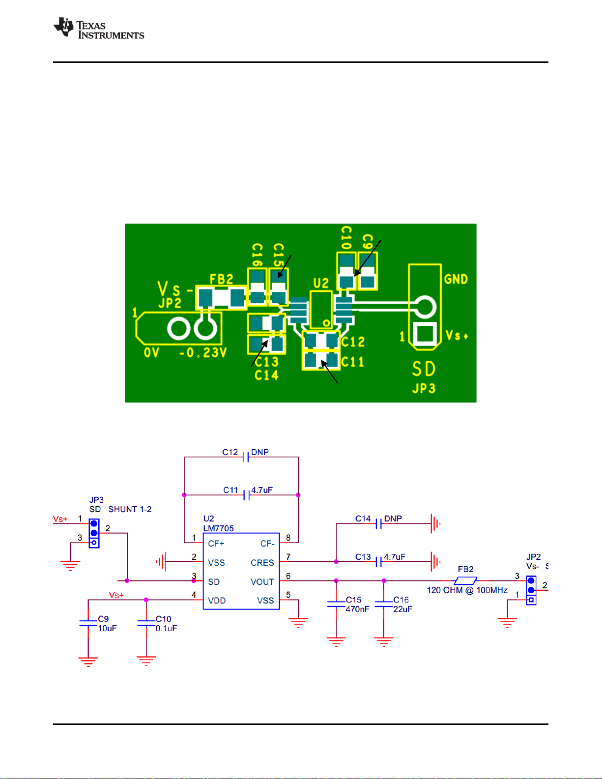
10.2 Layout Examples
Figure 35 contains a layout example for the LM7705.
RES
and C
in combination with short traces.
OUT
Figure 35. Example PCB Layout: Top layer
Figure 36. Schematics for Example PCB Layout
Product Folder Links: LM7705
Submit Documentation FeedbackCopyright © 2008–2018, Texas Instruments Incorporated
19
Page 20
LM7705
SNVS420D –NOVEMBER 2008–REVISED MAY 2018
www.ti.com
11 Device and Documentation Support
11.1 Community Resources
The following links connect to TI community resources. Linked contents are provided "AS IS" by the respective
contributors. They do not constitute TI specifications and do not necessarily reflect TI's views; see TI's Terms of
Use.
TI E2E™ Online Community TI's Engineer-to-Engineer (E2E) Community. Created to foster collaboration
among engineers. At e2e.ti.com, you can ask questions, share knowledge, explore ideas and help
solve problems with fellow engineers.
Design Support TI's Design Support Quickly find helpful E2E forums along with design support tools and
contact information for technical support.
11.2 Trademarks
E2E is a trademark of Texas Instruments.
All other trademarks are the property of their respective owners.
11.3 Electrostatic Discharge Caution
These devices have limited built-in ESD protection. The leads should be shorted together or the device placed in conductive foam
during storage or handling to prevent electrostatic damage to the MOS gates.
11.4 Glossary
SLYZ022 — TI Glossary.
This glossary lists and explains terms, acronyms, and definitions.
12 Mechanical, Packaging, and Orderable Information
The following pages include mechanical, packaging, and orderable information. This information is the most
current data available for the designated devices. This data is subject to change without notice and revision of
this document. For browser-based versions of this data sheet, refer to the left-hand navigation.
20
Submit Documentation Feedback Copyright © 2008–2018, Texas Instruments Incorporated
Product Folder Links: LM7705
Page 21
PACKAGE OPTION ADDENDUM
www.ti.com
10-Dec-2020
PACKAGING INFORMATION
Orderable Device Status
LM7705MM/NOPB ACTIVE VSSOP DGK 8 1000 RoHS & Green SN Level-1-260C-UNLIM -40 to 125 F26A
LM7705MME/NOPB ACTIVE VSSOP DGK 8 250 RoHS & Green SN Level-1-260C-UNLIM -40 to 125 F26A
LM7705MMX/NOPB ACTIVE VSSOP DGK 8 3500 RoHS & Green SN Level-1-260C-UNLIM -40 to 125 F26A
(1)
The marketing status values are defined as follows:
ACTIVE: Product device recommended for new designs.
LIFEBUY: TI has announced that the device will be discontinued, and a lifetime-buy period is in effect.
NRND: Not recommended for new designs. Device is in production to support existing customers, but TI does not recommend using this part in a new design.
PREVIEW: Device has been announced but is not in production. Samples may or may not be available.
OBSOLETE: TI has discontinued the production of the device.
Package Type Package
(1)
Drawing
Pins Package
Qty
Eco Plan
(2)
Lead finish/
Ball material
(6)
MSL Peak Temp
(3)
Op Temp (°C) Device Marking
(4/5)
(2)
RoHS: TI defines "RoHS" to mean semiconductor products that are compliant with the current EU RoHS requirements for all 10 RoHS substances, including the requirement that RoHS substance
do not exceed 0.1% by weight in homogeneous materials. Where designed to be soldered at high temperatures, "RoHS" products are suitable for use in specified lead-free processes. TI may
reference these types of products as "Pb-Free".
RoHS Exempt: TI defines "RoHS Exempt" to mean products that contain lead but are compliant with EU RoHS pursuant to a specific EU RoHS exemption.
Green: TI defines "Green" to mean the content of Chlorine (Cl) and Bromine (Br) based flame retardants meet JS709B low halogen requirements of <=1000ppm threshold. Antimony trioxide based
flame retardants must also meet the <=1000ppm threshold requirement.
(3)
MSL, Peak Temp. - The Moisture Sensitivity Level rating according to the JEDEC industry standard classifications, and peak solder temperature.
(4)
There may be additional marking, which relates to the logo, the lot trace code information, or the environmental category on the device.
(5)
Multiple Device Markings will be inside parentheses. Only one Device Marking contained in parentheses and separated by a "~" will appear on a device. If a line is indented then it is a continuation
of the previous line and the two combined represent the entire Device Marking for that device.
(6)
Lead finish/Ball material - Orderable Devices may have multiple material finish options. Finish options are separated by a vertical ruled line. Lead finish/Ball material values may wrap to two
lines if the finish value exceeds the maximum column width.
Important Information and Disclaimer:The information provided on this page represents TI's knowledge and belief as of the date that it is provided. TI bases its knowledge and belief on information
provided by third parties, and makes no representation or warranty as to the accuracy of such information. Efforts are underway to better integrate information from third parties. TI has taken and
continues to take reasonable steps to provide representative and accurate information but may not have conducted destructive testing or chemical analysis on incoming materials and chemicals.
TI and TI suppliers consider certain information to be proprietary, and thus CAS numbers and other limited information may not be available for release.
Samples
Addendum-Page 1
Page 22
PACKAGE OPTION ADDENDUM
www.ti.com
In no event shall TI's liability arising out of such information exceed the total purchase price of the TI part(s) at issue in this document sold by TI to Customer on an annual basis.
10-Dec-2020
Addendum-Page 2
Page 23
PACKAGE MATERIALS INFORMATION
www.ti.com 21-Oct-2021
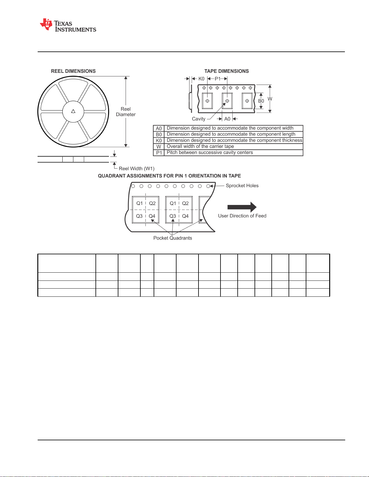
TAPE AND REEL INFORMATION
*All dimensions are nominal
Device Package
LM7705MM/NOPB VSSOP DGK 8 1000 178.0 12.4 5.3 3.4 1.4 8.0 12.0 Q1
LM7705MME/NOPB VSSOP DGK 8 250 178.0 12.4 5.3 3.4 1.4 8.0 12.0 Q1
LM7705MMX/NOPB VSSOP DGK 8 3500 330.0 12.4 5.3 3.4 1.4 8.0 12.0 Q1
Type
Package
Drawing
Pins SPQ Reel
Diameter
(mm)
Reel
Width
W1 (mm)
A0
(mm)B0(mm)K0(mm)P1(mm)W(mm)
Pin1
Quadrant
Pack Materials-Page 1
Page 24
PACKAGE MATERIALS INFORMATION
www.ti.com 21-Oct-2021
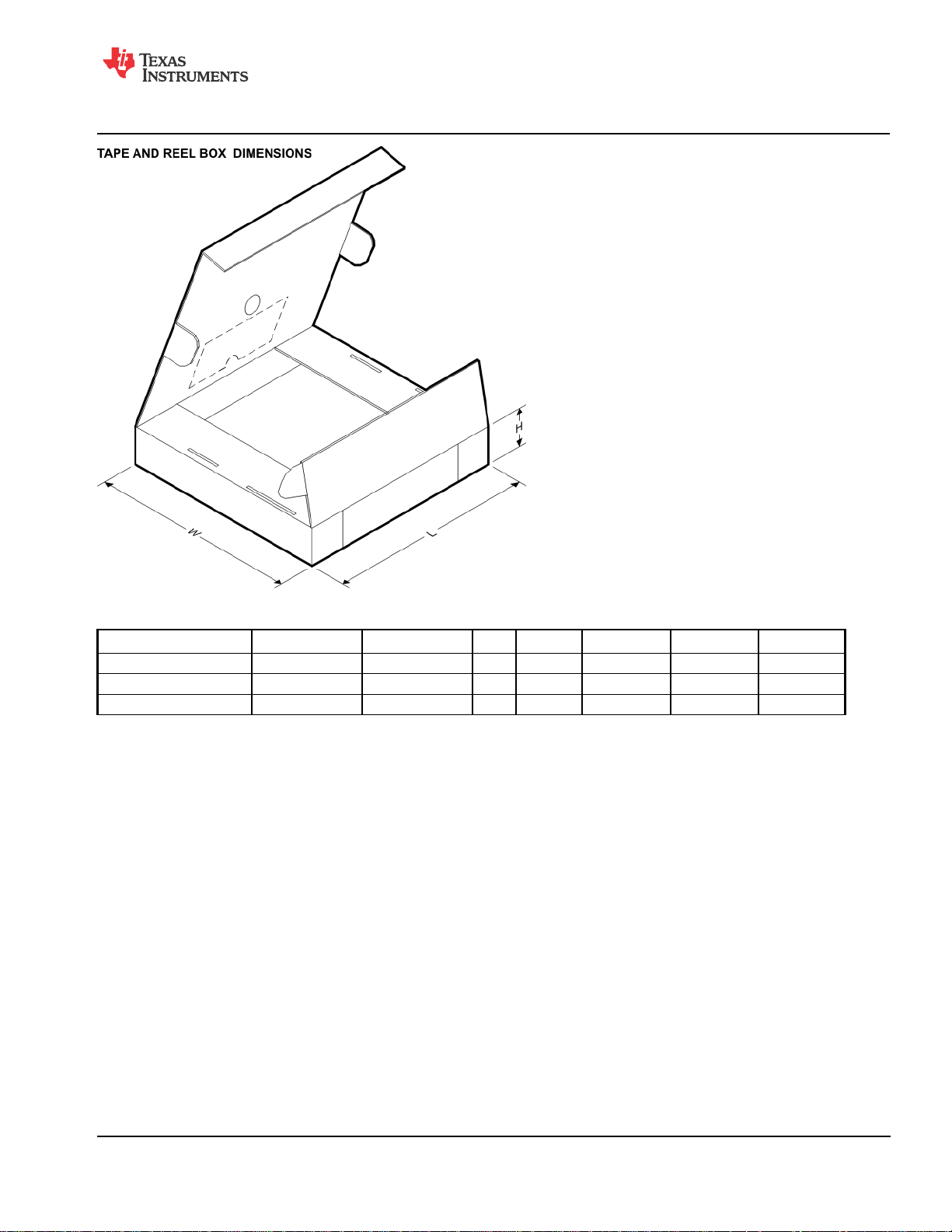
*All dimensions are nominal
Device Package Type Package Drawing Pins SPQ Length (mm) Width (mm) Height (mm)
LM7705MM/NOPB VSSOP DGK 8 1000 208.0 191.0 35.0
LM7705MME/NOPB VSSOP DGK 8 250 208.0 191.0 35.0
LM7705MMX/NOPB VSSOP DGK 8 3500 367.0 367.0 35.0
Pack Materials-Page 2
Page 25
Page 26
Page 27

IMPORTANT NOTICE AND DISCLAIMER
TI PROVIDES TECHNICAL AND RELIABILITY DATA (INCLUDING DATA SHEETS), DESIGN RESOURCES (INCLUDING REFERENCE
DESIGNS), APPLICATION OR OTHER DESIGN ADVICE, WEB TOOLS, SAFETY INFORMATION, AND OTHER RESOURCES “AS IS”
AND WITH ALL FAULTS, AND DISCLAIMS ALL WARRANTIES, EXPRESS AND IMPLIED, INCLUDING WITHOUT LIMITATION ANY
IMPLIED WARRANTIES OF MERCHANTABILITY, FITNESS FOR A PARTICULAR PURPOSE OR NON-INFRINGEMENT OF THIRD
PARTY INTELLECTUAL PROPERTY RIGHTS.
These resources are intended for skilled developers designing with TI products. You are solely responsible for (1) selecting the appropriate
TI products for your application, (2) designing, validating and testing your application, and (3) ensuring your application meets applicable
standards, and any other safety, security, regulatory or other requirements.
These resources are subject to change without notice. TI grants you permission to use these resources only for development of an
application that uses the TI products described in the resource. Other reproduction and display of these resources is prohibited. No license
is granted to any other TI intellectual property right or to any third party intellectual property right. TI disclaims responsibility for, and you
will fully indemnify TI and its representatives against, any claims, damages, costs, losses, and liabilities arising out of your use of these
resources.
TI’s products are provided subject to TI’s Terms of Sale or other applicable terms available either on ti.com or provided in conjunction with
such TI products. TI’s provision of these resources does not expand or otherwise alter TI’s applicable warranties or warranty disclaimers for
TI products.
TI objects to and rejects any additional or different terms you may have proposed. IMPORTANT NOTICE
Mailing Address: Texas Instruments, Post Office Box 655303, Dallas, Texas 75265
Copyright © 2021, Texas Instruments Incorporated
 Loading...