

Page 1

LM4871
www.ti.com
SNAS002F –FEBRUARY 2000–REVISED MAY 2013
LM4871 3W Audio Power Amplifier with Shutdown Mode
Check for Samples: LM4871
1
FEATURES
2
• No Output Coupling Capacitors, Bootstrap
Capacitors, or Snubber Circuits Required
• Unity-gain Stable
• WSON, VSSOP, SOIC, or PDIP Packaging
• External Gain Configuration Capability
• Pin Compatible with the LM4861
APPLICATIONS
• Portable Computers
• Desktop Computers operate on low supply voltages from 2.0V to 5.5V.
• Low Voltage Audio Systems
KEY SPECIFICATIONS
• PO at 10% THD+N, 1kHz
– LM4871LD: 3Ω , 4Ω Loads; 3W (typ),
2.5 W (typ)
– All other LM4871 Packages: 8Ω load
1.5 W (typ)
• Shutdown Current 0.6µA (typ)
• Supply Voltage Range 2.0V to 5.5 V
• THD at 1kHz at 1W Continuous Average
Output Power into 8Ω 0.5% (max)
DESCRIPTION
The LM4871 is a mono bridged audio power amplifier
capable of delivering 3W of continuous average
power into a 3Ω load with less than 10% THD when
powered by a 5V power supply (see Note). To
conserve power in portable applications, the
LM4871's micropower shutdown mode (IQ= 0.6µA,
typ) is activated when VDDis applied to the
SHUTDOWN pin.
Boomer audio power amplifiers are designed
specifically to provide high power, high fidelity audio
output. They require few external components and
Since the LM4871 does not require output coupling
capacitors, bootstrap capacitors, or snubber
networks, it is ideally suited for low-power portable
systems that require minimum volume and weight.
Additional LM4871 features include thermal shutdown
protection, unity-gain stability, and external gain set.
Note: An LM4871LD that has been properly mounted
to a circuit board will deliver 3W into 3Ω (at 10%
THD). The other package options for the LM4871 will
deliver 1.5W into 8Ω (at 10% THD). See the
Application Information section for further information
concerning the LM4871LD, LM4871MM, LM4871M,
and the LM4871N.
Connection Diagrams
Figure 1. VSSOP, Small Outline, and PDIP Figure 2. WSON Package (Top View)
Package
Top View
See Package Number DGK0008A, D0008A, or
D0008E
1
Please be aware that an important notice concerning availability, standard warranty, and use in critical applications of
Texas Instruments semiconductor products and disclaimers thereto appears at the end of this data sheet.
2All trademarks are the property of their respective owners.
PRODUCTION DATA information is current as of publication date.
Products conform to specifications per the terms of the Texas
Instruments standard warranty. Production processing does not
necessarily include testing of all parameters.
See Package Number NGN0008A
Copyright © 2000–2013, Texas Instruments Incorporated
Page 2
LM4871
SNAS002F –FEBRUARY 2000–REVISED MAY 2013
Typical Application
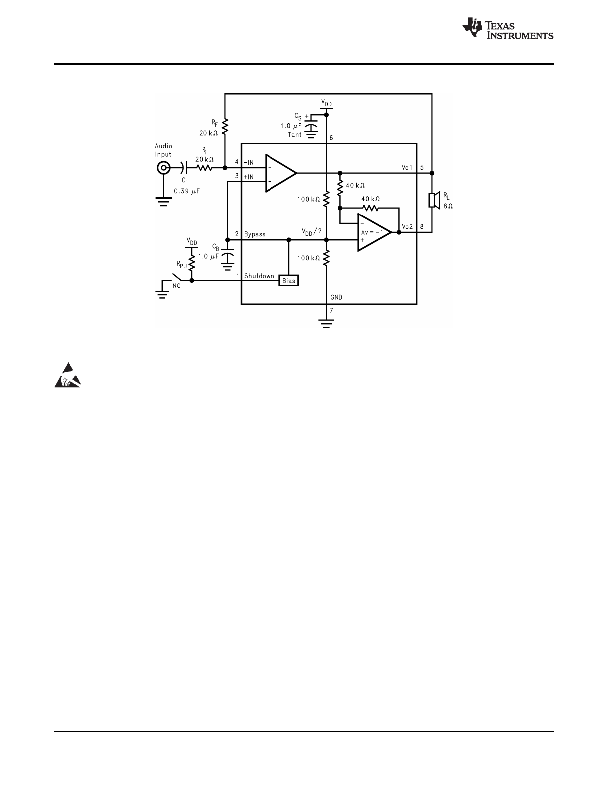
Figure 3. Typical Audio Amplifier Application Circuit
www.ti.com
These devices have limited built-in ESD protection. The leads should be shorted together or the device placed in conductive foam
during storage or handling to prevent electrostatic damage to the MOS gates.
2 Submit Documentation Feedback Copyright © 2000–2013, Texas Instruments Incorporated
Product Folder Links: LM4871
Page 3

LM4871
www.ti.com
Absolute Maximum Ratings
(1)(2)
SNAS002F –FEBRUARY 2000–REVISED MAY 2013
Supply Voltage 6.0V
Supply Temperature −65°C to +150°C
Input Voltage −0.3V to VDDto +0.3V
Power Dissipation
ESD Susceptibility
ESD Susceptibility
(3)
(4)
(5)
Internally Limited
5000V
250V
Junction Temperature 150°C
Soldering Information Small Outline Package Vapor Phase (60 sec.) 215°C
Infrared (15 sec.) 220°C
θ
(typ)—D0008A 35°C/W
JC
θ
(typ)—D0008A 140°C/W
JA
θ
(typ)—D0008E 37°C/W
JC
θ
(typ)—D0008E 107°C/W
JA
θ
(typ)—DGK0008A 56°C/W
JC
θ
(typ)—DGK0008A 210°C/W
JA
θ
(typ)—NGN0008A 4.3°C/W
JC
θ
(typ)—NGN0008A 56°C/W
JA
(1) Absolute Maximum Ratings indicate limits beyond which damage to the device may occur. Operating Ratings indicate conditions for
which the device is functional, but do not ensure specific performance limits. Electrical Characteristics state DC and AC electrical
specifications under particular test conditions which ensure specific performance limits. This assumes that the device is within the
Operating Ratings. Specifications are not ensured for parameters where no limit is given, however, the typical value is a good indication
of device performance.
(2) If Military/Aerospace specified devices are required, please contact the Texas Instruments Sales Office/Distributors for availability and
specifications.
(3) The maximum power dissipation must be derated at elevated temperatures and is dictated by T
TA. The maximum allowable power dissipation is P
is lower. For the LM4871, T
absolute maximum ratings section.
= 150°C. For the θJA's for different packages, please see the Application Information section or the
JMAX
DMAX
= (T
)/θJAor the number given in Absolute Maximum Ratings, whichever
JMAX–TA
, θJA, and the ambient temperature
JMAX
(4) Human body model, 100pF discharged through a 1.5kΩ resistor.
(5) Machine Model, 220pF–240pF discharged through all pins.
(6) The given θJAis for an LM4871 packaged in an NGN0008A with the Exposed–DAP soldered to an exposed 1in2area of 1oz printed
circuit board copper.
(6)
Operating Ratings
Temperature Range T
Supply Voltage 2.0V ≤ VDD≤ 5.5V
Electrical Characteristics
The following specifications apply for VDD= 5V and RL= 8Ω unless otherwise specified. Limits apply for TA= 25°C.
Symbol Parameter Conditions
V
DD
I
DD
I
SD
V
OS
(1) Absolute Maximum Ratings indicate limits beyond which damage to the device may occur. Operating Ratings indicate conditions for
(2) All voltages are measured with respect to the ground pin, unless otherwise specified.
(3) Typicals are specified at 25°C and represent the parametric norm.
(4) Limits are specified to TI's AOQL (Average Outgoing Quality Level).
Copyright © 2000–2013, Texas Instruments Incorporated Submit Documentation Feedback 3
Supply Voltage 2.0 5.5 V
Quiescent Power Supply VIN= 0V, Io= 0A 6.5 10.0 mA
Current
Shutdown Current V
Output Offset Voltage VIN= 0V 5.0 50 mV
which the device is functional, but do not ensure specific performance limits. Electrical Characteristics state DC and AC electrical
specifications under particular test conditions which ensure specific performance limits. This assumes that the device is within the
Operating Ratings. Specifications are not ensured for parameters where no limit is given, however, the typical value is a good indication
of device performance.
MIN
≤ TA≤ T
MAX
(1)(2)
PIN1
= V
DD
Product Folder Links: LM4871
Min
−40°C ≤ TA≤ 85°C
LM4871
(3)
Typical
(4)
Limit
(3)
Units
(Limits)
0.6 2 µA
Page 4
LM4871
SNAS002F –FEBRUARY 2000–REVISED MAY 2013
Electrical Characteristics
(1)(2)
(continued)
www.ti.com
The following specifications apply for VDD= 5V and RL= 8Ω unless otherwise specified. Limits apply for TA= 25°C.
LM4871
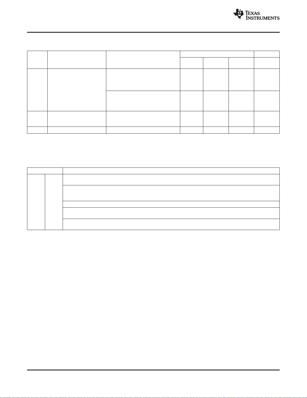
Symbol Parameter Conditions
P
o
Output Power THD = 1%, f = 1kHz
LM4871LD, RL= 3Ω
LM4871LD, RL= 4Ω
LM4871, RL= 8Ω
(5)
THD+N = 10%, f = 1kHz
LM4871LD, RL= 3Ω
LM4871LD, RL= 4Ω
LM4871, RL= 8Ω
(5)
(3)
Min
(5)
(5)
Typical
2.38
2
(4)
Limit
(3)
1.2
(5)
(5)
3
2.5
1.5
Units
(Limits)
THD+N Total Harmonic 20Hz ≤ f ≤ 20kHz, AVD= 2
Distortion+Noise LM4871LD, RL= 4Ω, PO= 1.6W 0.13 %
LM4871, RL= 8Ω, PO= 1W 0.25
PSRR Power Supply Rejection Ratio VDD= 4.9V to 5.1V 60 dB
(5) When driving 3Ω or 4Ω loads from a 5V supply, the LM4871LD must be mounted to a circuit board.
External Components Description
(Figure 3)
Components Functional Description
1. RiInverting input resistance that sets the closed-loop gain in conjunction with Rf. This resistor also forms a high pass filter
2. CiInput coupling capacitor that blocks the DC voltage at the amplifiers input terminals. Also creates a highpass filter with
3. RfFeedback resistance that sets the closed-loop gain in conjunction with Ri.
4. CSSupply bypass capacitor that provides power supply filtering. Refer to the Power Supply Bypassing section for
5. CBBypass pin capacitor that provides half-supply filtering. Refer to the section, Proper Selection of External Components,
with Ciat fC= 1/(2π RiCi).
Riat fc= 1/(2π RiCi). Refer to the section, Proper Selection of External Components, for an explanation of how to
determine the value of Ci.
information concerning proper placement and selection of the supply bypass capacitor.
for information concerning proper placement and selection of CB.
W
W
4 Submit Documentation Feedback Copyright © 2000–2013, Texas Instruments Incorporated
Product Folder Links: LM4871
Page 5

LM4871
www.ti.com
SNAS002F –FEBRUARY 2000–REVISED MAY 2013
Typical Performance Characteristics
NGN Specific Characteristics
LM4871LD THD+N vs Output Power LM4871LD THD+N vs Frequency
Figure 4. Figure 5.
LM4871LD THD+N vs Frequency LM4871LD THD+N vs Output Power
Figure 6. Figure 7.
LM4871LD Power Dissipation vs Output Power LM4871LD Power Derating Curve
This curve shows the LM4871LD's thermal dissipation ability at
different ambient temperatures given the exposed-DAP of the part is
soldered to a plane of 1oz. Cu with an area given in the label of each
curve. This label also designates whether the plane exists on the
same (top) layer as the chip, on the bottom layer, or on both layers.
Infinite heatsink and unattached (no heatsink) conditions are also
Figure 8. Figure 9.
shown.
Copyright © 2000–2013, Texas Instruments Incorporated Submit Documentation Feedback 5
Product Folder Links: LM4871
Page 6
LM4871
SNAS002F –FEBRUARY 2000–REVISED MAY 2013
Typical Performance Characteristics
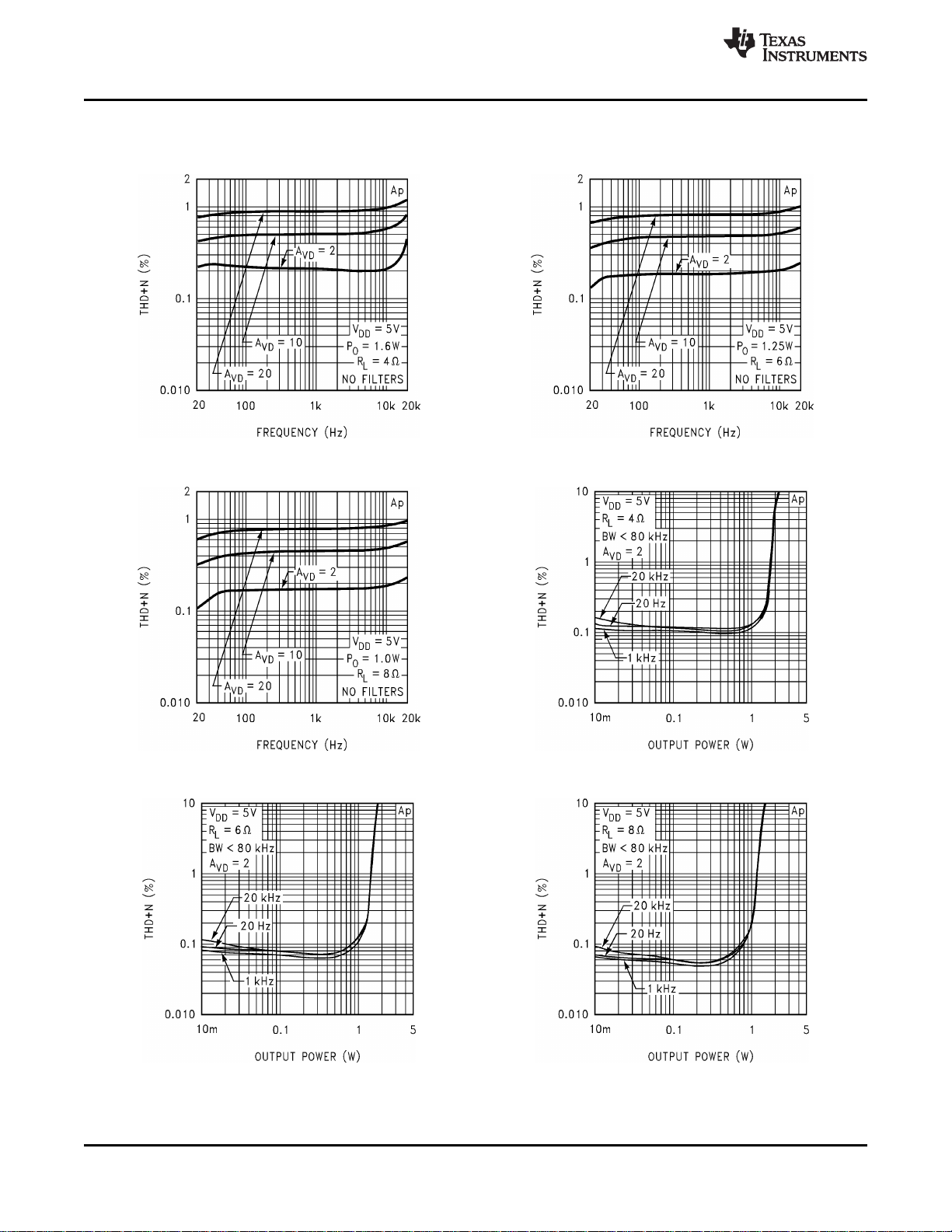
THD+N vs Frequency THD+N vs Frequency
Figure 10. Figure 11.
THD+N vs Frequency THD+N vs Output Power
www.ti.com
Non-NGN Specific Characteristics
Figure 12. Figure 13.
THD+N vs Output Power THD+N vs Output Power
Figure 14. Figure 15.
6 Submit Documentation Feedback Copyright © 2000–2013, Texas Instruments Incorporated
Product Folder Links: LM4871
Page 7
LM4871
www.ti.com
SNAS002F –FEBRUARY 2000–REVISED MAY 2013
Typical Performance Characteristics
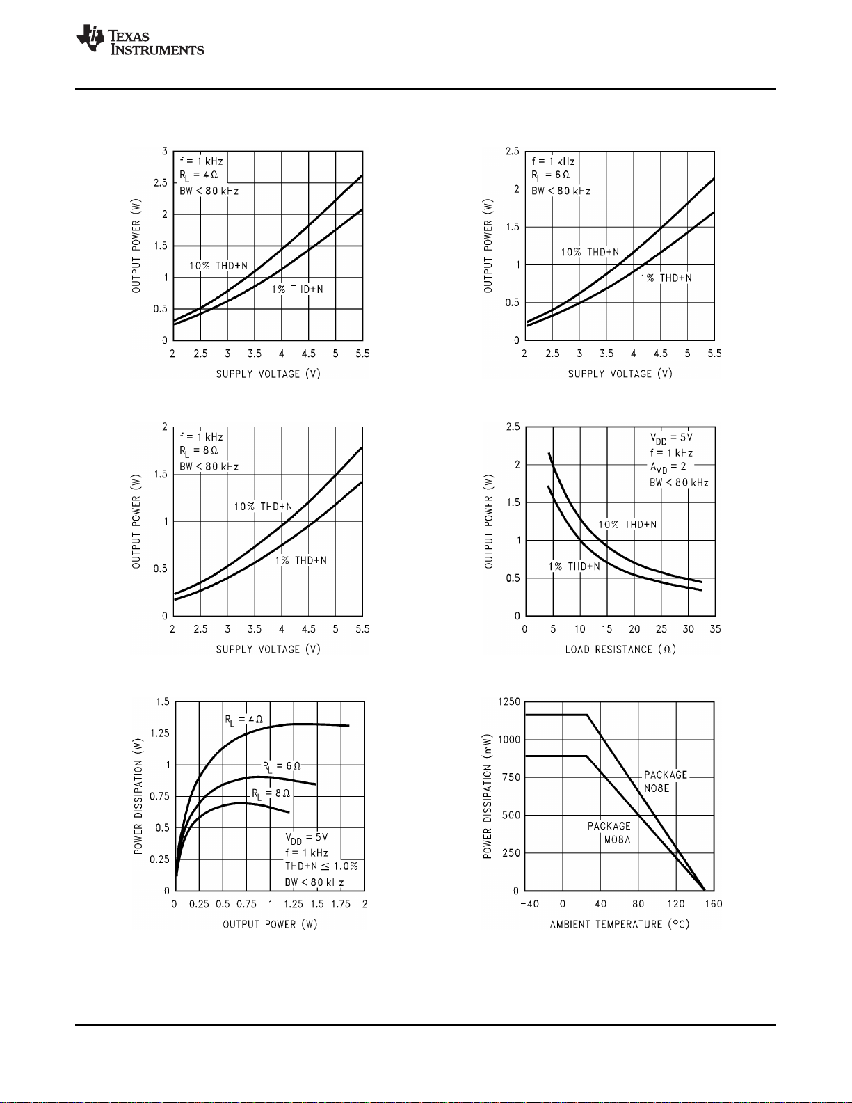
Output Power vs Supply Voltage Output Power vs Supply Voltage
Output Power vs Supply Voltage Output Power vs Load Resistance
Non-NGN Specific Characteristics (continued)
Figure 16. Figure 17.
Figure 18. Figure 19.
Power Dissipation vs Output Power Power Derating Curve
Figure 20. Figure 21.
Copyright © 2000–2013, Texas Instruments Incorporated Submit Documentation Feedback 7
Product Folder Links: LM4871
Page 8
LM4871
SNAS002F –FEBRUARY 2000–REVISED MAY 2013
Typical Performance Characteristics
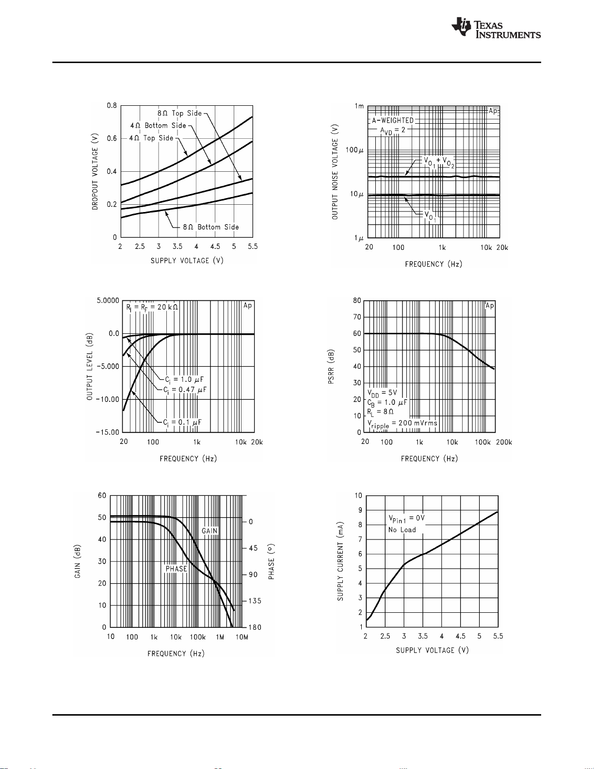
Clipping Voltage vs Supply Voltage Noise Floor
Frequency Response vs Input Capacitor Size Power Supply Rejection Ratio
Non-NGN Specific Characteristics (continued)
Figure 22. Figure 23.
www.ti.com
Figure 24. Figure 25.
Open Loop Frequency Response Supply Current vs Supply Voltage
Figure 26. Figure 27.
8 Submit Documentation Feedback Copyright © 2000–2013, Texas Instruments Incorporated
Product Folder Links: LM4871
Page 9

LM4871
www.ti.com
SNAS002F –FEBRUARY 2000–REVISED MAY 2013
APPLICATION INFORMATION
EXPOSED-DAP PACKAGE PCB MOUNTING CONSIDERATION
The LM4871's exposed-DAP (die attach paddle) package (NGN) provides a low thermal resistance between the
die and the PCB to which the part is mounted and soldered. This allows rapid heat transfer from the die to the
surrounding PCB copper traces, ground plane, and surrounding air. The result is a low voltage audio power
amplifier that produces 2W at ≤ 1% THD with a 4Ω load. This high power is achieved through careful
consideration of necessary thermal design. Failing to optimize thermal design may compromise the LM4871's
high power performance and activate unwanted, though necessary, thermal shutdown protection.
The NGN package must have its DAP soldered to a copper pad on the PCB. The DAP's PCB copper pad is
connected to a large plane of continuous unbroken copper. This plane forms a thermal mass, heat sink, and
radiation area. Place the heat sink area on either outside plane in the case of a two-sided PCB, or on an inner
layer of a board with more than two layers. Connect the DAP copper pad to the inner layer or backside copper
heat sink area with 4(2x2) vias. The via diameter should be 0.012in-0.013in with a 1.27mm pitch. Ensure efficient
thermal conductivity by plating through the vias.
Best thermal performance is achieved with the largest practical heat sink area. If the heatsink and amplifier share
the same PCB layer, a nominal 2.5in2area is necessary for 5V operation with a 4Ω load. Heatsink areas not
placed on the same PCB layer as the LM4871 should be 5in2(min) for the same supply voltage and load
resistance. The last two area recommendations apply for 25°C ambient temperature. Increase the area to
compensate for ambient temperatures above 25°C. The LM4871's power de-rating curve in the Typical
Performance Characteristics shows the maximum power dissipation versus temperature. An example PCB layout
for the NGN package is shown in the Demonstration Board Layout section. Further detailed and specific
information concerning PCB layout, fabrication, and mounting an NGN (WSON) package is available from TI's
Package Engineering Group under application note AN-1187 (Literature Number SNOA401).
PCB LAYOUT AND SUPPLY REGULATION CONSIDERATIONS FOR DRIVING 3Ω AND 4Ω LOADS
Power dissipated by a load is a function of the voltage swing across the load and the load's impedance. As load
impedance decreases, load dissipation becomes increasingly dependant on the interconnect (PCB trace and
wire) resistance between the amplifier output pins and the load's connections. Residual trace resistance causes
a voltage drop, which results in power dissipated in the trace and not in the load as desired. For example, 0.1Ω
trace resistance reduces the output power dissipated by a 4Ω load from 2.0W to 1.95W. This problem of
decreased load dissipation is exacerbated as load impedance decreases. Therefore, to maintain the highest load
dissipation and widest output voltage swing, PCB traces that connect the output pins to a load must be as wide
as possible.
Poor power supply regulation adversely affects maximum output power. A poorly regulated supply's output
voltage decreases with increasing load current. Reduced supply voltage causes decreased headroom, output
signal clipping, and reduced output power. Even with tightly regulated supplies, trace resistance creates the
same effects as poor supply regulation. Therefore, making the power supply traces as wide as possible helps
maintain full output voltage swing.
BRIDGE CONFIGURATION EXPLANATION
As shown in Figure 3, the LM4871 has two operational amplifiers internally, allowing for a few different amplifier
configurations. The first amplifier's gain is externally configurable; the second amplifier is internally fixed in a
unity-gain, inverting configuration. The closed-loop gain of the first amplifier is set by selecting the ratio of Rfto R
while the second amplifier's gain is fixed by the two internal 40kΩ resistors. Figure 3 shows that the output of
amplifier one serves as the input to amplifier two, which results in both amplifiers producing signals identical in
magnitude, but 180° out of phase. Consequently, the differential gain for the IC is
AVD= 2 *(Rf/Ri) (1)
By driving the load differentially through outputs Vo1 and Vo2, an amplifier configuration commonly referred to as
“bridged mode” is established. Bridged mode operation is different from the classical single-ended amplifier
configuration where one side of its load is connected to ground.
i
Copyright © 2000–2013, Texas Instruments Incorporated Submit Documentation Feedback 9
Product Folder Links: LM4871
Page 10

LM4871
SNAS002F –FEBRUARY 2000–REVISED MAY 2013
www.ti.com
A bridge amplifier design has a few distinct advantages over the single-ended configuration, as it provides
differential drive to the load, thus doubling output swing for a specified supply voltage. Four times the output
power is possible as compared to a single-ended amplifier under the same conditions. This increase in attainable
output power assumes that the amplifier is not current limited or clipped. In order to choose an amplifier's closedloop gain without causing excessive clipping, please refer to the Audio Power Amplifier Design section.
Another advantage of the differential bridge output is no net DC voltage across load. This results from biasing
VO1 and VO2 at the same DC voltage, in this case VDD/2 . This eliminates the coupling capacitor that single
supply, single-ended amplifiers require. Eliminating an output coupling capacitor in a single-ended configuration
forces a single supply amplifier's half-supply bias voltage across the load. The current flow created by the halfsupply bias voltage increases internal IC power dissipation and my permanently damage loads such as
speakers.
POWER DISSIPATION
Power dissipation is a major concern when designing a successful amplifier, whether the amplifier is bridged or
single-ended. A direct consequence of the increased power delivered to the load by a bridge amplifier is an
increase in internal power dissipation. Equation 2 states the maximum power dissipation point for a bridge
amplifier operating at a given supply voltage and driving a specified output load.
P
= 4*(VDD)2/(2π2RL) (2)
DMAX
Since the LM4871 has two operational amplifiers in one package, the maximum internal power dissipation is 4
times that of a single-ended ampifier. Even with this substantial increase in power dissipation, the LM4871 does
not require heatsinking under most operating conditions and output loading. From Equation 2, assuming a 5V
power supply and an 8Ω load, the maximum power dissipation point is 625 mW. The maximum power dissipation
point obtained from Equation 2 must not be greater than the power dissipation that results from Equation 3:
P
= (T
DMAX
For the SOIC package, θJA= 140°C/W, for the PDIP package, θJA= 107°C/W, and for the VSSOP package, θ
= 210°C/W assuming free air operation. For the NGN package soldered to a DAP pad that expands to a copper
area of 1.0in2on a PCB, the LM4871's θJAis 56°C/W. T
by using some form of heat sinking. The resultant θJAwill be the summation of the θJC, θCS, and θSA. θJCis the
junction to case of the package (or to the exposed DAP, as is the case with the NGN package), θCSis the case
to heat sink thermal resistance and θSAis the heat sink to ambient thermal resistance. By adding additional
copper area around the LM4871, the θJAcan be reduced from its free air value for the SOIC and VSSOP
packages. Increasing the copper area around the NGN package from 1.0in2to 2.0in2area results in a θ
decrease to 46°C/W. Depending on the ambient temperature, TA, and the θJA, Equation 3 can be used to find the
maximum internal power dissipation supported by the IC packaging. If the result of Equation 2 is greater than
that of Equation 3, then either the supply voltage must be decreased, the load impedance increased, the θ
decreased, or the ambient temperature reduced. For the typical application of a 5V power supply, with an 8Ω
load, and no additional heatsinking, the maximum ambient temperature possible without violating the maximum
junction temperature is approximately 61°C provided that device operation is around the maximum power
dissipation point and assuming surface mount packaging. For the NGN package in a typical application of a 5V
power supply, with a 4Ω load, and 1.0in2copper area soldered to the exposed DAP pad, the maximum ambient
temperature is approximately 77°C providing device operation is around the maximum power dissipation point.
Internal power dissipation is a function of output power. If typical operation is not around the maximum power
dissipation point, the ambient temperature can be increased. Refer to the Typical Performance Characteristics
curves for power dissipation information for different output powers and output loading.
JMAX–TA
)/θ
JA
= 150°C for the LM4871. The θJAcan be decreased
JMAX
(3)
JA
JA
JA
POWER SUPPLY BYPASSING
As with any amplifier, proper supply bypassing is critical for low noise performance and high power supply
rejection. The capacitor location on both the bypass and power supply pins should be as close to the LM4871 as
possible. The capacitor connected between the bypass pin and ground improves the internal bias voltage's
stability, producing improved PSRR. The improvements to PSRR increase as the bypass pin capacitor increases.
Typical applications employ a 5V regulator with 10µF and a 0.1µF bypass capacitors which aid in supply stability.
This does not eliminate the need for bypassing the supply nodes of the LM4871 with a 1µF tantalum capacitor.
The selection of bypass capacitors, especially CB, is dependent upon PSRR requirements, click and pop
performance as explained in the section, Proper Selection of External Components, system cost, and size
constraints.
10 Submit Documentation Feedback Copyright © 2000–2013, Texas Instruments Incorporated
Product Folder Links: LM4871
Page 11

LM4871
www.ti.com
SNAS002F –FEBRUARY 2000–REVISED MAY 2013
SHUTDOWN FUNCTION
In order to reduce power consumption while not in use, the LM4871 contains a shutdown pin to externally turn off
the amplifier's bias circuitry. This shutdown feature turns the amplifier off when a logic high is placed on the
shutdown pin. The trigger point between a logic low and logic high level is typically half- supply. It is best to
switch between ground and supply to provide maximum device performance. By switching the shutdown pin to
VDD, the LM4871 supply current draw will be minimized in idle mode. While the device will be disabled with
shutdown pin voltages less then VDD, the idle current may be greater than the typical value of 0.6µA. In either
case, the shutdown pin should be tied to a definite voltage to avoid unwanted state changes.
In many applications, a microcontroller or microprocessor output is used to control the shutdown circuitry which
provides a quick, smooth transition into shutdown. Another solution is to use a single-pole, single-throw switch in
conjunction with an external pull-up resistor. When the switch is closed, the shutdown pin is connected to ground
and enables the amplifier. If the switch is open, then the external pull-up resistor will disable the LM4871. This
scheme ensures that the shutdown pin will not float thus preventing unwanted state changes.
PROPER SELECTION OF EXTERNAL COMPONENTS
Proper selection of external components in applications using integrated power amplifiers is critical to optimize
device and system performance. While the LM4871 is tolerant of external component combinations,
consideration to component values must be used to maximize overall system quality.
The LM4871 is unity-gain stable which gives a designer maximum system flexibility. The LM4871 should be used
in low gain configurations to minimize THD+N values, and maximize the signal to noise ratio. Low gain
configurations require large input signals to obtain a given output power. Input signals equal to or greater than 1
Vrms are available from sources such as audio codecs. Please refer to the section, Audio Power Amplifier
Design, for a more complete explanation of proper gain selection.
Besides gain, one of the major considerations is the closed-loop bandwidth of the amplifier. To a large extent, the
bandwidth is dictated by the choice of external components shown in Audio Power Amplifier Design. The input
coupling capacitor, Ci, forms a first order high pass filter which limits low frequency response. This value should
be chosen based on needed frequency response for a few distinct reasons.
Selection Of Input Capacitor Size
Large input capacitors are both expensive and space hungry for portable designs. Clearly, a certain sized
capacitor is needed to couple in low frequencies without severe attenuation. But in many cases the speakers
used in portable systems, whether internal or external, have little ability to reproduce signals below 100Hz to
150Hz. Thus, using a large input capacitor may not increase actual system performance.
In addition to system cost and size, click and pop performance is effected by the size of the input coupling
capacitor, Ci.A larger input coupling capacitor requires more charge to reach its quiescent DC voltage (nominally
1/2 VDD). This charge comes from the output via the feedback and is apt to create pops upon device enable.
Thus, by minimizing the capacitor size based on necessary low frequency response, turn-on pops can be
minimized.
Besides minimizing the input capacitor size, careful consideration should be paid to the bypass capacitor value.
Bypass capacitor, CB, is the most critical component to minimize turn-on pops since it determines how fast the
LM4871 turns on. The slower the LM4871's outputs ramp to their quiescent DC voltage (nominally 1/2 VDD), the
smaller the turn-on pop. Choosing CBequal to 1.0µF along with a small value of Ci(in the range of 0.1µF to
0.39µF), should produce a virtually clickless and popless shutdown function. While the device will function
properly, (no oscillations or motorboating), with CBequal to 0.1µF, the device will be much more susceptible to
turn-on clicks and pops. Thus, a value of CBequal to 1.0µF is recommended in all but the most cost sensitive
designs.
Copyright © 2000–2013, Texas Instruments Incorporated Submit Documentation Feedback 11
Product Folder Links: LM4871
Page 12
LM4871
SNAS002F –FEBRUARY 2000–REVISED MAY 2013
www.ti.com
AUDIO POWER AMPLIFIER DESIGN
Design a 1W/8Ω Audio Amplifier
Given:
Power Output 1 Wrms
Load Impedance 8Ω
Input Level 1 Vrms
Input Impedance 20 kΩ
Bandwidth 100 Hz–20 kHz ± 0.25 dB
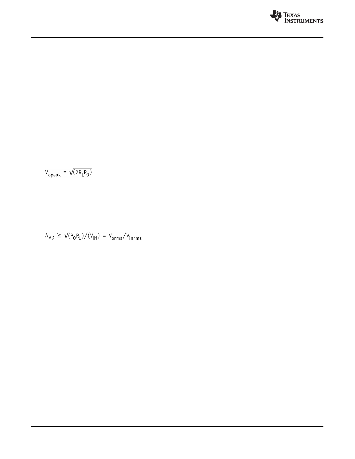
A designer must first determine the minimum supply rail to obtain the specified output power. By extrapolating
from the Output Power vs Supply Voltage graphs in the Typical Performance Characteristics section, the supply
rail can be easily found. A second way to determine the minimum supply rail is to calculate the required V
using Equation 4 and add the output voltage. Using this method, the minimum supply voltage would be (V
(V
OD
TOP
+ V
OD
BOT
)), where V
OD
BOT
and V
are extrapolated from the Dropout Voltage vs Supply Voltage curve in
TOP
OD
the Typical Performance Characteristics section.
Using the Output Power vs Supply Voltage graph for an 8Ω load, the minimum supply rail is 4.6V. But since 5V is
a standard voltage in most applications, it is chosen for the supply rail. Extra supply voltage creates headroom
that allows the LM4871 to reproduce peaks in excess of 1W without producing audible distortion. At this time, the
designer must make sure that the power supply choice along with the output impedance does not violate the
conditions explained in the POWER DISSIPATION section.
Once the power dissipation equations have been addressed, the required differential gain can be determined
from Equation 5.
opeak
opeak
(4)
+
(5)
Rf/Ri= AVD/2 (6)
From Equation 5, the minimum AVDis 2.83; use AVD= 3.
Since the desired input impedance was 20kΩ, and with a AVDimpedance of 2, a ratio of 1.5:1 of Rfto Riresults
in an allocation of Ri= 20kΩ and Rf= 30kΩ. The final design step is to address the bandwidth requirements
which must be stated as a pair of −3dB frequency points. Five times away from a −3dB point is 0.17dB down
from passband response which is better than the required ±0.25dB specified.
fL= 100Hz/5 = 20Hz
fH= 20kHz * 5 = 100kHz
As stated in the External Components Description section, Riin conjunction with Cicreate a highpass filter.
Ci≥ 1/(2π*20kΩ*20Hz) = 0.397µF; use 0.39µF
The high frequency pole is determined by the product of the desired frequency pole, fH, and the differential gain,
AVD. With a AVD= 3 and fH= 100kHz, the resulting GBWP = 150kHz which is much smaller than the LM4871
GBWP of 4MHz. This figure displays that if a designer has a need to design an amplifier with a higher differential
gain, the LM4871 can still be used without running into bandwidth limitations.
12 Submit Documentation Feedback Copyright © 2000–2013, Texas Instruments Incorporated
Product Folder Links: LM4871
Page 13
LM4871
www.ti.com
SNAS002F –FEBRUARY 2000–REVISED MAY 2013
Demonstration Board Layout
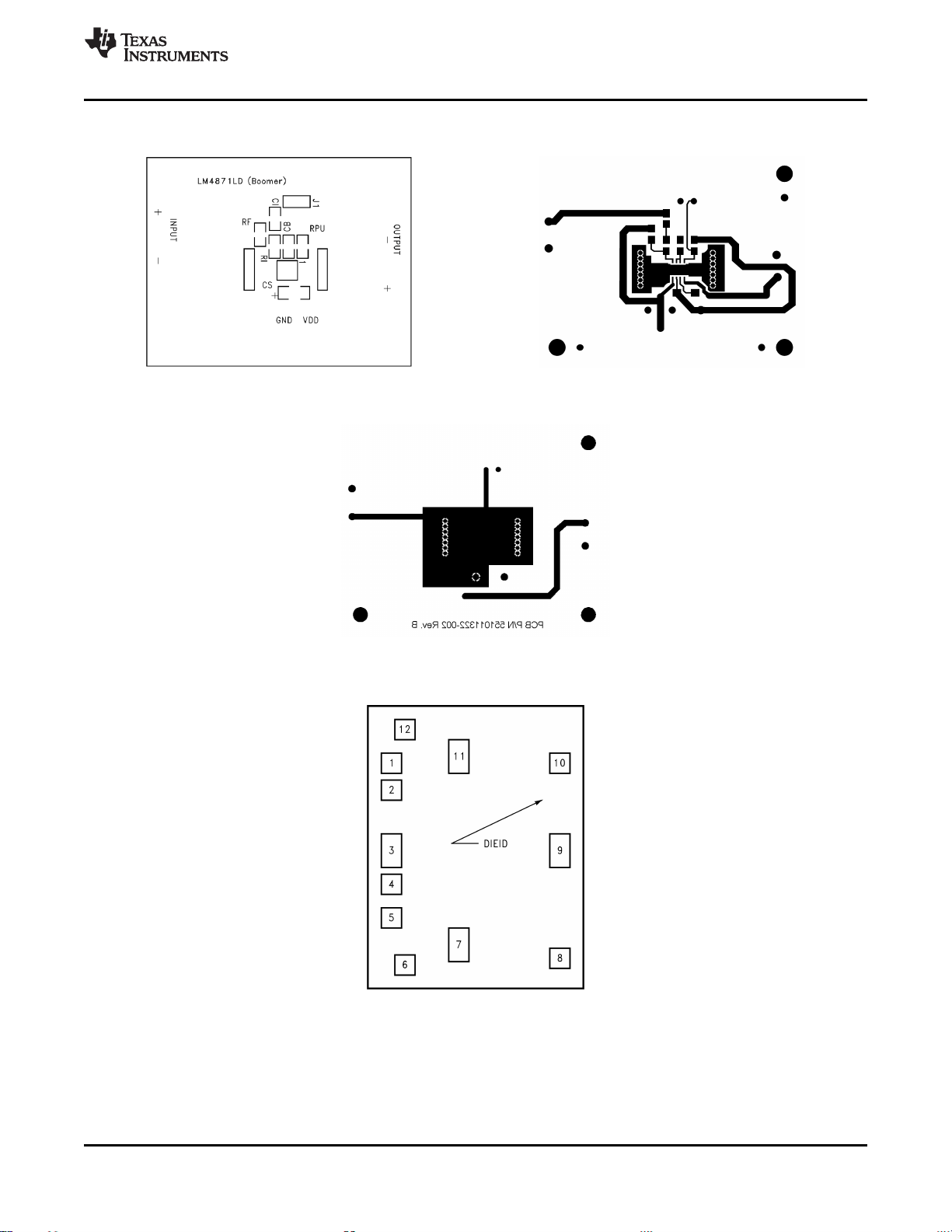
Figure 28. Recommended NGN PC Board Layout: Figure 29. Recommended NGN PC Board Layout:
Component-Side Silkscreen Component-Side Layout
Figure 30. Recommended NGN PC Board Layout: Bottom-Side Layout
LM4871 MDA MWA 3W Audio Power Amplifier With Shutdown Mode
Figure 31. Die Layout (C - Step)
Copyright © 2000–2013, Texas Instruments Incorporated Submit Documentation Feedback 13
Product Folder Links: LM4871
Page 14

LM4871
SNAS002F –FEBRUARY 2000–REVISED MAY 2013
www.ti.com
Die/Wafer Characteristics
Fabrication Attributes General Die Information
Physical Die Identification LM4871C Bond Pad Opening Size (min) 102µm x 102µm
Die Step C Bond Pad Metalization 0.5% COPPER_BAL.
Physical Attributes Passivation NITRIDE
Wafer Diameter 150mm Back Side Metal BARE BACK
Dise Size (Drawn) 1372µm x 1758µm Back Side Connection GND
Thickness 406µm Nominal
Min Pitch 164µm Nominal
Special Assembly Requirements:
Note: Actual die size is rounded to the nearest micron.
(Referenced to die center, coordinates in µm) NC = No Connection
SIGNAL NAME PAD# NUMBER
SHUTDOWN 1 -559 541 102 x 102
BYPASS 2 -559 376 102 x 102
NC 3 -559 -45 102 x 210
INPUT + 4 -559 -248 102 x 102
INPUT - 5 -559 -486 102 x 102
GND 6 -476 -725 102 x 102
VOUT 1 7 -135 -598 102 x 210
GND 8 554 -686 102 x 102
VDD 9 554 -4 102 x 210
GND 10 554 568 102 x 102
VOUT 2 11 -135 598 102 x 210
GND 12 -473 752 102 x 102
54mils x 69mils
Die Bond Pad Coordinate Locations (C - Step)
X/Y COORDINATES PAD SIZE
X Y X Y
ALUMINUM
14 Submit Documentation Feedback Copyright © 2000–2013, Texas Instruments Incorporated
Product Folder Links: LM4871
Page 15

LM4871
www.ti.com
SNAS002F –FEBRUARY 2000–REVISED MAY 2013
REVISION HISTORY
Changes from Revision E (May 2013) to Revision F Page
• Changed layout of National Data Sheet to TI format .......................................................................................................... 14
Copyright © 2000–2013, Texas Instruments Incorporated Submit Documentation Feedback 15
Product Folder Links: LM4871
Page 16
PACKAGE OPTION ADDENDUM
www.ti.com
30-Sep-2021
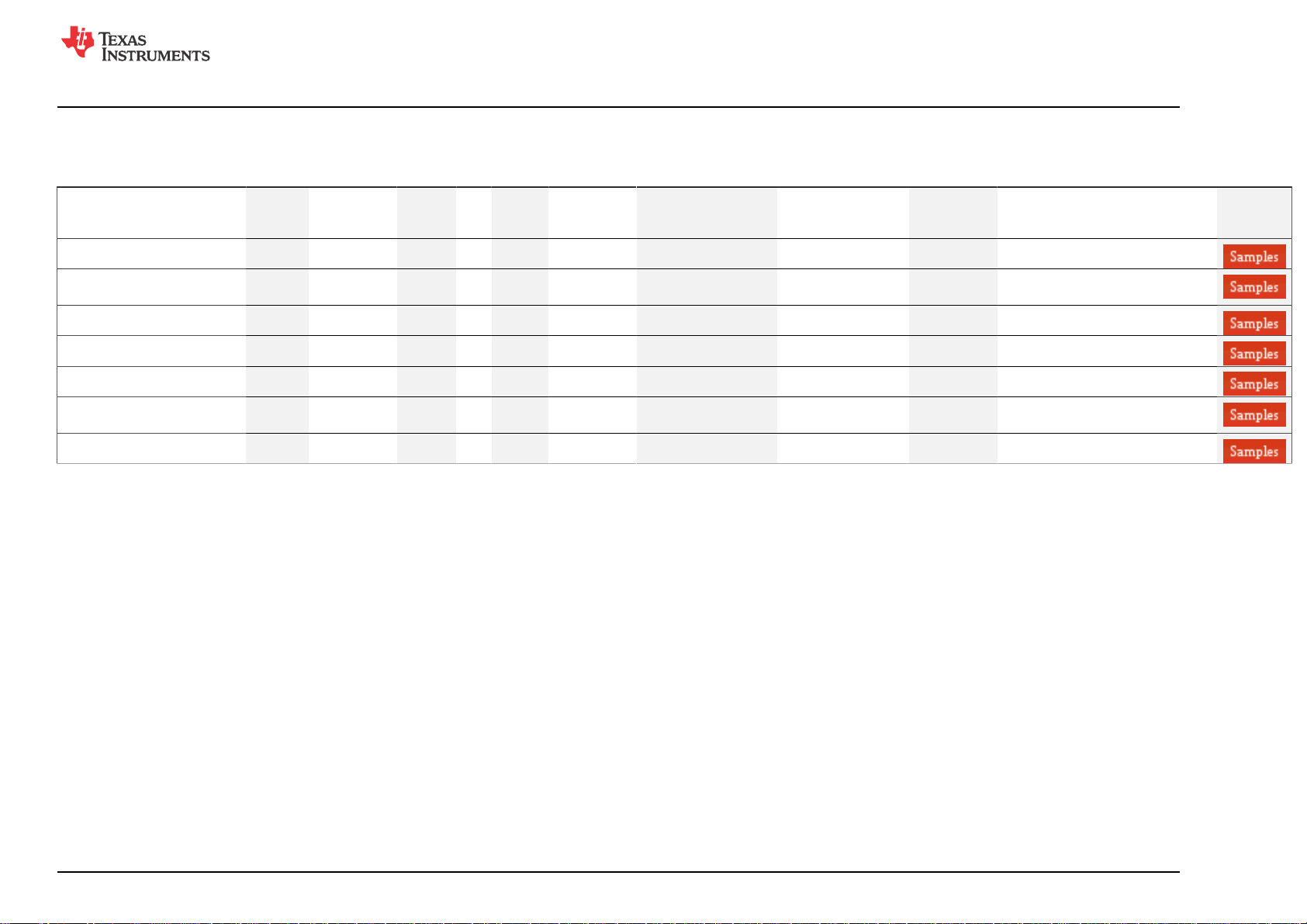
PACKAGING INFORMATION
Orderable Device Status
LM4871LD/NOPB ACTIVE WSON NGN 8 1000 RoHS & Green SN Level-3-260C-168 HR -40 to 85 L4871
LM4871M ACTIVE SOIC D 8 95 Non-RoHS
LM4871M/NOPB ACTIVE SOIC D 8 95 RoHS & Green SN Level-1-260C-UNLIM -40 to 85 4871
LM4871MM/NOPB ACTIVE VSSOP DGK 8 1000 RoHS & Green SN Level-1-260C-UNLIM -40 to 85 G71
LM4871MMX/NOPB ACTIVE VSSOP DGK 8 3500 RoHS & Green SN Level-1-260C-UNLIM -40 to 85 G71
LM4871MX ACTIVE SOIC D 8 2500 Non-RoHS
LM4871MX/NOPB ACTIVE SOIC D 8 2500 RoHS & Green SN Level-1-260C-UNLIM -40 to 85 4871
(1)
The marketing status values are defined as follows:
ACTIVE: Product device recommended for new designs.
LIFEBUY: TI has announced that the device will be discontinued, and a lifetime-buy period is in effect.
NRND: Not recommended for new designs. Device is in production to support existing customers, but TI does not recommend using this part in a new design.
PREVIEW: Device has been announced but is not in production. Samples may or may not be available.
OBSOLETE: TI has discontinued the production of the device.
Package Type Package
(1)
Drawing
Pins Package
Qty
Eco Plan
(2)
& Green
& Green
Lead finish/
Ball material
(6)
Call TI Level-1-235C-UNLIM -40 to 85 4871
Call TI Level-1-235C-UNLIM -40 to 85 4871
MSL Peak Temp
(3)
Op Temp (°C) Device Marking
(4/5)
(2)
RoHS: TI defines "RoHS" to mean semiconductor products that are compliant with the current EU RoHS requirements for all 10 RoHS substances, including the requirement that RoHS substance
do not exceed 0.1% by weight in homogeneous materials. Where designed to be soldered at high temperatures, "RoHS" products are suitable for use in specified lead-free processes. TI may
reference these types of products as "Pb-Free".
RoHS Exempt: TI defines "RoHS Exempt" to mean products that contain lead but are compliant with EU RoHS pursuant to a specific EU RoHS exemption.
Green: TI defines "Green" to mean the content of Chlorine (Cl) and Bromine (Br) based flame retardants meet JS709B low halogen requirements of <=1000ppm threshold. Antimony trioxide based
flame retardants must also meet the <=1000ppm threshold requirement.
(3)
MSL, Peak Temp. - The Moisture Sensitivity Level rating according to the JEDEC industry standard classifications, and peak solder temperature.
(4)
There may be additional marking, which relates to the logo, the lot trace code information, or the environmental category on the device.
(5)
Multiple Device Markings will be inside parentheses. Only one Device Marking contained in parentheses and separated by a "~" will appear on a device. If a line is indented then it is a continuation
of the previous line and the two combined represent the entire Device Marking for that device.
Samples
Addendum-Page 1
Page 17

PACKAGE OPTION ADDENDUM
www.ti.com
(6)
Lead finish/Ball material - Orderable Devices may have multiple material finish options. Finish options are separated by a vertical ruled line. Lead finish/Ball material values may wrap to two
lines if the finish value exceeds the maximum column width.
30-Sep-2021
Important Information and Disclaimer:The information provided on this page represents TI's knowledge and belief as of the date that it is provided. TI bases its knowledge and belief on information
provided by third parties, and makes no representation or warranty as to the accuracy of such information. Efforts are underway to better integrate information from third parties. TI has taken and
continues to take reasonable steps to provide representative and accurate information but may not have conducted destructive testing or chemical analysis on incoming materials and chemicals.
TI and TI suppliers consider certain information to be proprietary, and thus CAS numbers and other limited information may not be available for release.
In no event shall TI's liability arising out of such information exceed the total purchase price of the TI part(s) at issue in this document sold by TI to Customer on an annual basis.
Addendum-Page 2
Page 18
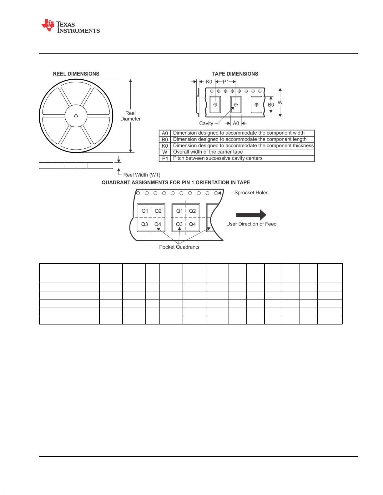
PACKAGE MATERIALS INFORMATION
www.ti.com 5-Jan-2022
TAPE AND REEL INFORMATION
*All dimensions are nominal
Device Package
LM4871LD/NOPB WSON NGN 8 1000 178.0 12.4 4.3 4.3 1.3 8.0 12.0 Q1
LM4871MM/NOPB VSSOP DGK 8 1000 178.0 12.4 5.3 3.4 1.4 8.0 12.0 Q1
LM4871MMX/NOPB VSSOP DGK 8 3500 330.0 12.4 5.3 3.4 1.4 8.0 12.0 Q1
LM4871MX SOIC D 8 2500 330.0 12.4 6.5 5.4 2.0 8.0 12.0 Q1
LM4871MX/NOPB SOIC D 8 2500 330.0 12.4 6.5 5.4 2.0 8.0 12.0 Q1
Type
Package
Drawing
Pins SPQ Reel
Diameter
(mm)
Reel
Width
W1 (mm)
A0
(mm)B0(mm)K0(mm)P1(mm)W(mm)
Pin1
Quadrant
Pack Materials-Page 1
Page 19

PACKAGE MATERIALS INFORMATION
www.ti.com 5-Jan-2022
*All dimensions are nominal
Device Package Type Package Drawing Pins SPQ Length (mm) Width (mm) Height (mm)
LM4871LD/NOPB WSON NGN 8 1000 208.0 191.0 35.0
LM4871MM/NOPB VSSOP DGK 8 1000 208.0 191.0 35.0
LM4871MMX/NOPB VSSOP DGK 8 3500 367.0 367.0 35.0
LM4871MX SOIC D 8 2500 367.0 367.0 35.0
LM4871MX/NOPB SOIC D 8 2500 367.0 367.0 35.0
Pack Materials-Page 2
Page 20
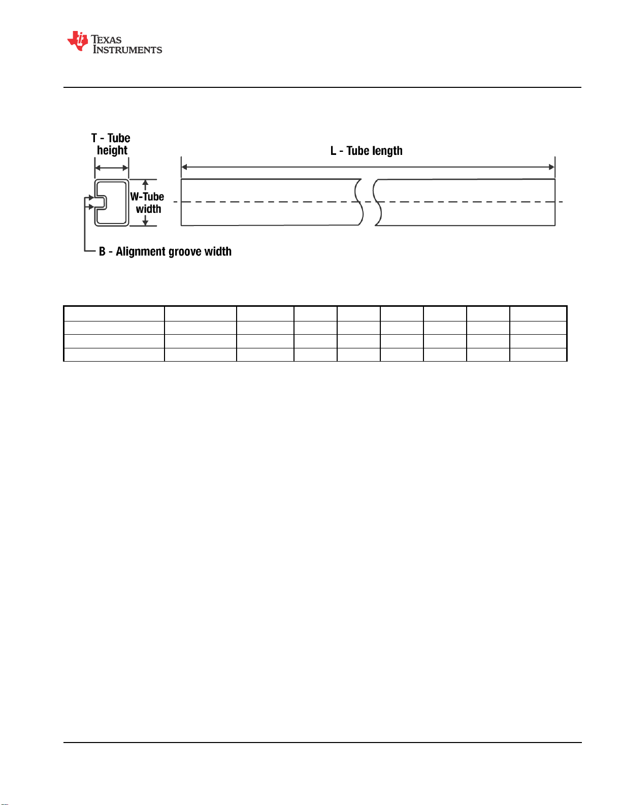
PACKAGE MATERIALS INFORMATION
www.ti.com 5-Jan-2022
TUBE
*All dimensions are nominal
Device Package Name Package Type Pins SPQ L (mm) W (mm) T (µm) B (mm)
LM4871M D SOIC 8 95 495 8 4064 3.05
LM4871M D SOIC 8 95 495 8 4064 3.05
LM4871M/NOPB D SOIC 8 95 495 8 4064 3.05
Pack Materials-Page 3
Page 21

PACKAGE OUTLINE
PIN 1 INDEX AREA
0.8 MAX
0.05
0.00
SCALE 3.000
A
4.1
3.9
B
4.1
3.9
WSON - 0.8 mm max heightNGN0008A
PLASTIC SMALL OUTLINE - NO LEAD
PIN 1 ID
DETAIL A
PIN 1 ID
C
SEATING PLANE
0.08 C
2.2 0.05
EXPOSED
THERMAL PAD
6X 0.8
2X
2.4
SEE
DETAIL A
(0.25)
(0.25)
PIN 1 ID
4
1
SYMM
(0.2)
(0.15)
(0.2) TYP
5
9
0.6
8X
0.4
SYMM
8
3 0.05
0.35
8X
0.25
0.1 C A B
0.05
C
4214794/A 11/2019
NOTES:
1. All linear dimensions are in millimeters. Any dimensions in parenthesis are for reference only. Dimensioning and tolerancing
per ASME Y14.5M.
2. This drawing is subject to change without notice.
3. The package thermal pad must be soldered to the printed circuit board for thermal and mechanical performance.
www.ti.com
Page 22
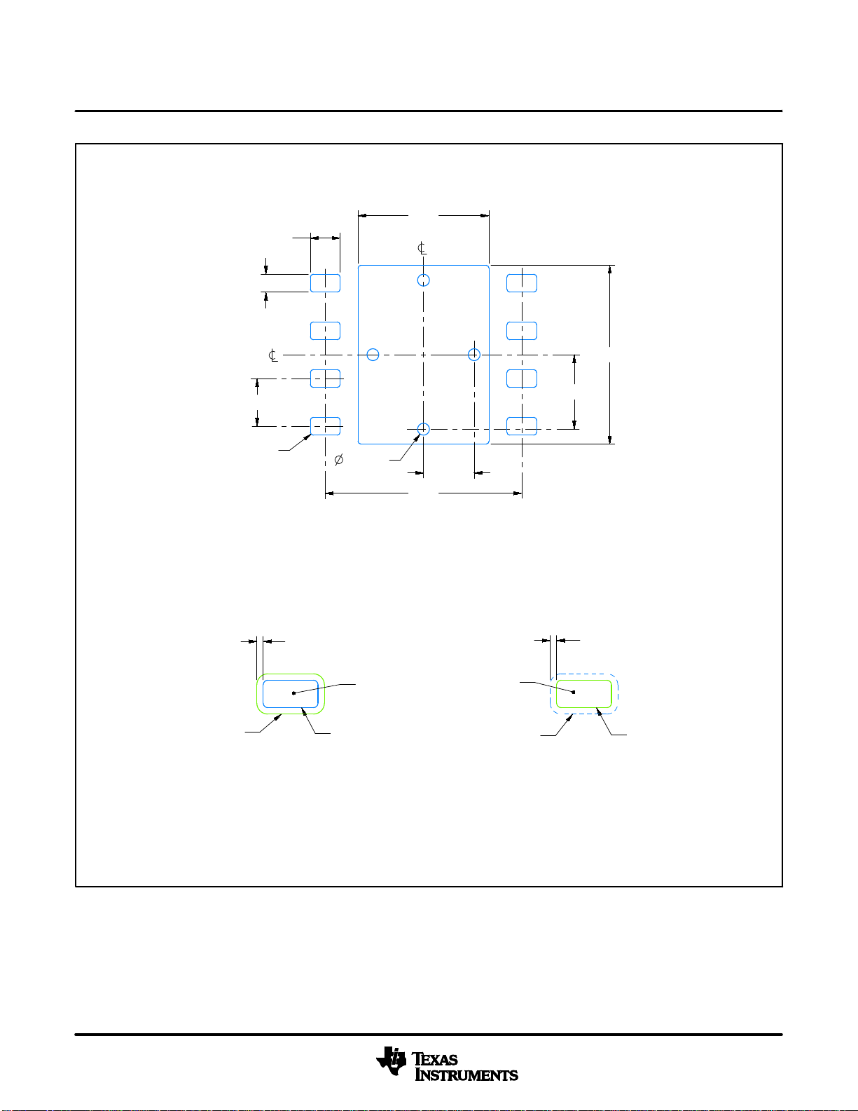
8X (0.5)
8X (0.3)
EXAMPLE BOARD LAYOUT
WSON - 0.8 mm max heightNGN0008A
PLASTIC SMALL OUTLINE - NO LEAD
(2.2)
SYMM
1
8
(R0.05) TYP
SOLDER MASK
OPENING
SYMM
6X (0.8)
4
( 0.2) VIA
TYP
0.07 MAX
ALL AROUND
METAL
NON SOLDER MASK
DEFINED
(PREFERRED)
9
(0.85)
(3.3)
LAND PATTERN EXAMPLE
EXPOSED METAL SHOWN
SCALE:15X
EXPOSED
METAL
EXPOSED
METAL
METAL UNDER
SOLDER MASK
(3)
(1.25)
5
0.07 MIN
ALL AROUND
SOLDER MASK
OPENING
SOLDER MASK
DEFINED
SOLDER MASK DETAILS
4214794/A 11/2019
NOTES: (continued)
4. This package is designed to be soldered to a thermal pad on the board. For more information, see Texas Instruments literature
number SLUA271 (www.ti.com/lit/slua271).
5. Vias are optional depending on application, refer to device data sheet. If any vias are implemented, refer to their locations shown
on this view. It is recommended that vias under paste be filled, plugged or tented.
www.ti.com
Page 23
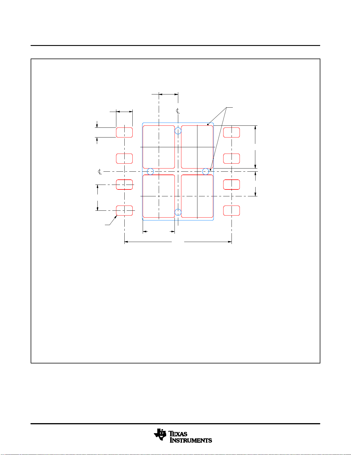
0.59
EXAMPLE STENCIL DESIGN
WSON - 0.8 mm max heightNGN0008A
PLASTIC SMALL OUTLINE - NO LEAD
8X (0.5)
8X (0.3)
SYMM
6X (0.8)
(R0.05) TYP
SYMM
1
9
4
4X (0.98)
(3.3)
METAL
TYP
8
5
SOLDER PASTE EXAMPLE
BASED ON 0.125 mm THICK STENCIL
EXPOSED PAD 9:
78% PRINTED SOLDER COVERAGE BY AREA UNDER PACKAGE
SCALE:20X
4X (1.31)
(0.755)
4214794/A 11/2019
NOTES: (continued)
6. Laser cutting apertures with trapezoidal walls and rounded corners may offer better paste release. IPC-7525 may have alternate
design recommendations.
www.ti.com
Page 24
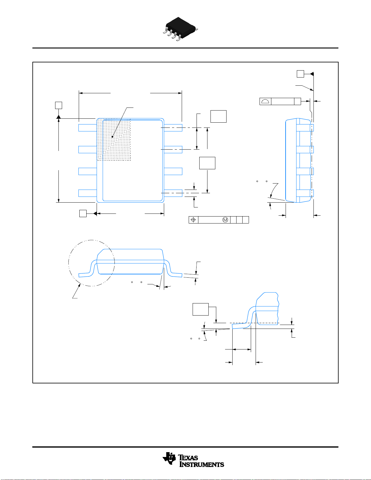
PACKAGE OUTLINE
A
.189-.197
[4.81-5.00]
NOTE 3
.228-.244 TYP
[5.80-6.19]
1
4
B .150-.157
[3.81-3.98]
PIN 1 ID AREA
NOTE 4
SCALE 2.800
6X .050
[1.27]
8
2X
.150
[3.81]
5
8X .012-.020
[0.31-0.51]
.010 [0.25] C A B
SOIC - 1.75 mm max heightD0008A
SMALL OUTLINE INTEGRATED CIRCUIT
C
SEATING PLANE
.004 [0.1] C
4X (0 -15 )
.069 MAX
[1.75]
.005-.010 TYP
[0.13-0.25]
4X (0 -15 )
SEE DETAIL A
.010
[0.25]
0 - 8
.016-.050
[0.41-1.27]
(.041)
[1.04]
DETAIL A
TYPICAL
.004-.010
[0.11-0.25]
4214825/C 02/2019
NOTES:
1. Linear dimensions are in inches [millimeters]. Dimensions in parenthesis are for reference only. Controlling dimensions are in inches.
Dimensioning and tolerancing per ASME Y14.5M.
2. This drawing is subject to change without notice.
3. This dimension does not include mold flash, protrusions, or gate burrs. Mold flash, protrusions, or gate burrs shall not
exceed .006 [0.15] per side.
4. This dimension does not include interlead flash.
5. Reference JEDEC registration MS-012, variation AA.
www.ti.com
Page 25
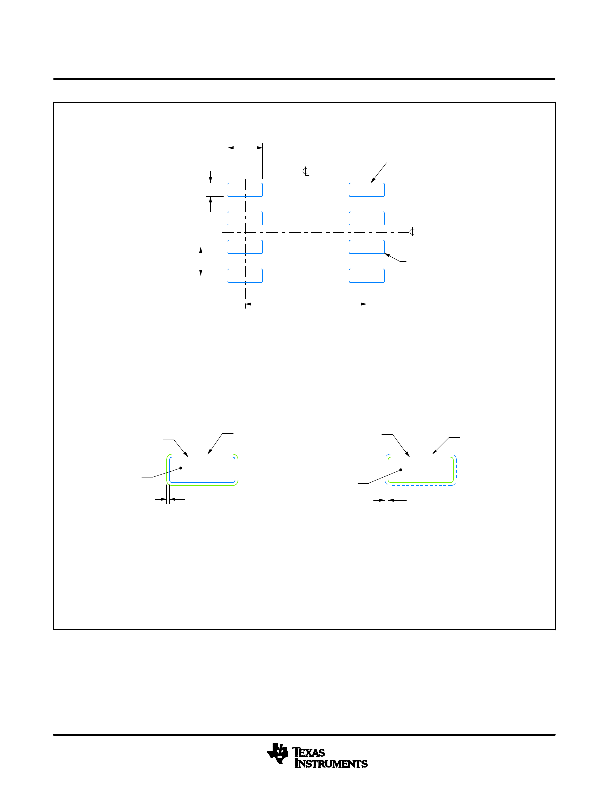
8X (.061 )
8X (.024)
6X (.050 )
[1.27]
[0.6]
[1.55]
SYMM
1
4
(.213)
[5.4]
LAND PATTERN EXAMPLE
EXPOSED METAL SHOWN
SCALE:8X
EXAMPLE BOARD LAYOUT
SOIC - 1.75 mm max heightD0008A
SMALL OUTLINE INTEGRATED CIRCUIT
SEE
DETAILS
8
SYMM
(R.002 ) TYP
5
[0.05]
EXPOSED
METAL
METAL
NON SOLDER MASK
SOLDER MASK
OPENING
.0028 MAX
[0.07]
ALL AROUND
DEFINED
SOLDER MASK
OPENING
EXPOSED
METAL
.0028 MIN
[0.07]
ALL AROUND
SOLDER MASK
DEFINED
SOLDER MASK DETAILS
NOTES: (continued)
6. Publication IPC-7351 may have alternate designs.
7. Solder mask tolerances between and around signal pads can vary based on board fabrication site.
METAL UNDER
SOLDER MASK
4214825/C 02/2019
www.ti.com
Page 26
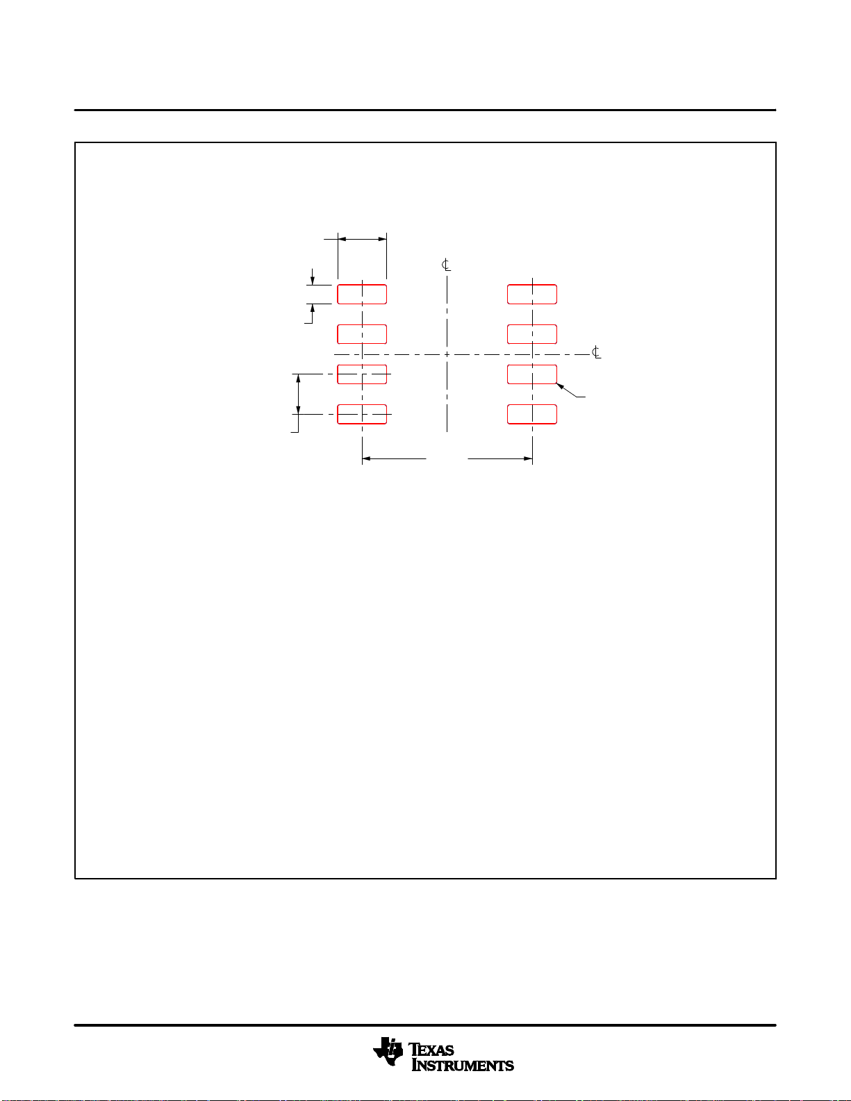
8X (.061 )
8X (.024)
[0.6]
6X (.050 )
[1.27]
[1.55]
EXAMPLE STENCIL DESIGN
SOIC - 1.75 mm max heightD0008A
SMALL OUTLINE INTEGRATED CIRCUIT
SYMM
1
8
SYMM
(R.002 ) TYP
4
(.213)
[5.4]
5
[0.05]
SOLDER PASTE EXAMPLE
BASED ON .005 INCH [0.125 MM] THICK STENCIL
NOTES: (continued)
8. Laser cutting apertures with trapezoidal walls and rounded corners may offer better paste release. IPC-7525 may have alternate
design recommendations.
9. Board assembly site may have different recommendations for stencil design.
SCALE:8X
4214825/C 02/2019
www.ti.com
Page 27
Page 28
Page 29

IMPORTANT NOTICE AND DISCLAIMER
TI PROVIDES TECHNICAL AND RELIABILITY DATA (INCLUDING DATA SHEETS), DESIGN RESOURCES (INCLUDING REFERENCE
DESIGNS), APPLICATION OR OTHER DESIGN ADVICE, WEB TOOLS, SAFETY INFORMATION, AND OTHER RESOURCES “AS IS”
AND WITH ALL FAULTS, AND DISCLAIMS ALL WARRANTIES, EXPRESS AND IMPLIED, INCLUDING WITHOUT LIMITATION ANY
IMPLIED WARRANTIES OF MERCHANTABILITY, FITNESS FOR A PARTICULAR PURPOSE OR NON-INFRINGEMENT OF THIRD
PARTY INTELLECTUAL PROPERTY RIGHTS.
These resources are intended for skilled developers designing with TI products. You are solely responsible for (1) selecting the appropriate
TI products for your application, (2) designing, validating and testing your application, and (3) ensuring your application meets applicable
standards, and any other safety, security, regulatory or other requirements.
These resources are subject to change without notice. TI grants you permission to use these resources only for development of an
application that uses the TI products described in the resource. Other reproduction and display of these resources is prohibited. No license
is granted to any other TI intellectual property right or to any third party intellectual property right. TI disclaims responsibility for, and you
will fully indemnify TI and its representatives against, any claims, damages, costs, losses, and liabilities arising out of your use of these
resources.
TI’s products are provided subject to TI’s Terms of Sale or other applicable terms available either on ti.com or provided in conjunction with
such TI products. TI’s provision of these resources does not expand or otherwise alter TI’s applicable warranties or warranty disclaimers for
TI products.
TI objects to and rejects any additional or different terms you may have proposed. IMPORTANT NOTICE
Mailing Address: Texas Instruments, Post Office Box 655303, Dallas, Texas 75265
Copyright © 2022, Texas Instruments Incorporated
 Loading...