

Page 1

TL/H/9059
LM196/LM396 10 Amp Adjustable Voltage Regulator
August 1992
LM196/LM396 10 Amp Adjustable Voltage Regulator
General Description
The LM196 is a 10 amp regulator, adjustable from 1.25V to
15V, which uses a revolutionary new IC fabrication structure
to combine high power discrete transistor technology with
modern monolithic linear IC processing. This combination
yields a high-performance single-chip regulator capable of
supplying in excess of 10 amps and operating at power levels up to 70 watts. The regulators feature on-chip trimming
of reference voltage to
g
0.8% and simultaneous trimming
of reference temperature drift to 30 ppm/
§
C typical. Thermal
interaction between control circuitry and the pass transistor
which affects the output voltage has been reduced to extremely low levels by strict attention to isothermal layout.
This interaction, called thermal regulation, is 100% tested.
These new regulators have all the protection features of
popular lower power adjustable regulators such as LM117
and LM138, including current limiting and thermal limiting.
The combination of these features makes the LM196 immune to blowout from output overloads or shorts, even if
the adjustment pin is accidentally disconnected. All devices
are ‘‘burned-in’’ in thermal shutdown to guarantee proper
operation of these protective features under actual overload
conditions.
Output voltage is continuously adjustable from 1.25V to
15V. Higher output voltages are possible if the maximum
input-output voltage differential specification is not exceeded. Full load current of 10A is available at all output voltages, subject only to the maximum power limit of 70W and
of course, maximum junction temperature.
The LM196 is exceptionally easy to use. Only two external
resistors are used to to set output voltage. On-chip adjustment of the reference voltage allows a much tighter specification of output voltage, eliminating any need for trimming in
most cases. The regulator will tolerate an extremely wide
range of reactive loads, and does not depend on external
capacitors for frequency stabilization. Heat sink requirements are much less stringent, because overload situations
do not have to be accounted forÐonly worst-case full load
conditions.
The LM196 is in a TO-3 package with oversized (0.060
×
)
leads to provide best possible load regulation. Operating
junction temperature range is
b
55§Ctoa150§C. The
LM396 is specified for a 0
§
Ctoa125§C junction tempera-
ture range.
Features
Y
Output pre-trimmed tog0.8%
Y
10A guaranteed output current
Y
PaProduct Enhancement tested
Y
70W maximum power dissipation
Y
Adjustable outputÐ1.25V to 15V
Y
Internal current and power limiting
Y
Guaranteed thermal resistance
Y
Output voltage guaranteed under worst-case conditions
Y
Output is short circuit protected
Typical Applications
V
OUT
e
(1.25V)
#
R1aR2
R1
J
a
I
ADJ
(R2)
TL/H/9059– 1
*For best TC of V
OUT
, R1 should be wirewound
or metal film, 1% or better.
**R2 should be same type as R1, with TC track-
ing of 30 ppm/
§
C or better.
²
C1 is necessary only if main filter capacitor is
more than 6
×
away, assumingÝ18 or larger
leads.
²²
C2 is not absolutely necessary, but is suggested to lower high frequency output impedance.
Output capacitors in the range of 1 mFto
1000 mF of aluminum or tantalum electrolytic
are commonly used to provide improved output impedance and rejection of transients.
Ê
C3 improves ripple rejection, output impedance, and noise. C2 should be 1 mF or larger
close to the regulator if C3 is used.
FIGURE 1. Basic 1.25V to 15V Regulator
C
1995 National Semiconductor Corporation RRD-B30M115/Printed in U. S. A.
Page 2

Absolute Maximum Ratings
If Military/Aerospace specified devices are required,
please contact the National Semiconductor Sales
Office/Distributors for availability and specifications.
Power Dissipation Internally Limited
Input-Output Voltage Differential 20V
Operating Junction Temperature Range
LM196 Control Section
b
55§Ctoa150§C
Power Transistor
b
55§Ctoa200§C
LM396 Control Section 0§Ctoa125§C
Power Transistor 0
§
Ctoa175§C
Storage Temperature
b
65§Ctoa150§C
Lead Temperature (Soldering, 10 seconds) 300§C
ESD rating to be determined
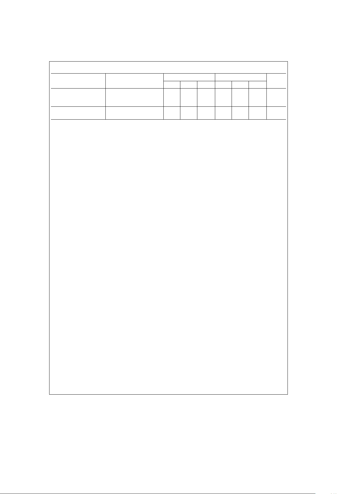
Electrical Characteristics (Note 1)
Parameter Conditions
LM196 LM396
Units
Min Typ Max Min Typ Max
Reference Voltage I
OUT
e
10 mA 1.24 1.25 1.26 1.23 1.25 1.27 V
Reference Voltage V
MIN
s
(V
IN
b
V
OUT
)s20V 1.22 1.25 1.28 1.21 1.25 1.29 V
(Note 2) 10 mA
s
I
OUT
10A, PsP
MAX
Full Temperature Range
Line Regulation V
MIN
s
(V
IN
b
V
OUT
)s20V 0.005 0.01 0.005 0.02 %/V
(Note 3) Full Temperature Range 0.05 0.05 %/V
Load Regulation 10 mAsI
OUT
s
10A 0.1 0.1 %/A
LM196/LM396 V
MIN
s
V
IN
b
V
OUT
s
10V, PsP
MAX
(Note 4) Full Temperature Range 0.15 0.15 %/A
Ripple Rejection C
ADJ
e
25 mF, fe120 Hz 60 74 66 74 dB
(Note 5) Full Temperature Range 54 54 dB
Thermal Regulation V
IN
b
V
OUT
e
5V, I
OUT
e
10A 0.003 0.005 0.003 0.015 %/W
(Note 6)
Average Output Voltage T
jMIN
s
T
j
s
T
jMAX
0.003 0.003 %/§C
Temperature Coefficient (See Curves for Limits)
Adjustment Pin Current 50 100 50 100 mA
Adjustment Pin Current 10 mAsI
OUT
s
10A 3 3 mA
Change (Note 7) 3V
s
V
IN
b
V
OUT
s
20V
PsP
MAX
, Full Temperature Range
Minimum Load Current 2.5Vs(V
IN
b
V
OUT
)s20V 10 10 mA
(Note 9) Full Temperature Range
Current Limit 2.5s(V
IN
b
V
OUT
s
7V 10 14 20 10 14 20 A
(Note 8) V
IN
b
V
OUT
e
20V 1.5 3 8 1.5 3 8 A
Rms Output Noise 10 Hzsfs10 kHz 0.001 0.001 %V
OUT
Long Term Stability T
j
e
125§C, te1000 Hours 0.3 1.0 0.3 1.0 %
Thermal Resistance Control Circuitry 0.3 0.5 0.3 0.5§C/W
Junction to Case Power Transistor 1.0 1.2 1.0 1.2
§
C/W
(Note 10)
2
Page 3
Electrical Characteristics (Note 1) (Continued)
Parameter Conditions
LM196 LM396
Units
Min Typ Max Min Typ Max
Power Dissipation (P
MAX
) 7.0VsV
IN
b
V
OUT
s
12V 70 100 70 100 W
(Note 11) V
IN
b
V
OUT
e
15V 50 50 W
V
IN
b
V
OUT
e
18V 36 36 W
Drop-Out Voltage I
OUT
e
10A, 2.1 2.5 2.1 2.5 V
LM196/LM396 Full Temperature Range 2.75 2.75
Note 1: Unless otherwise stated, these specifications apply for T
j
e
25§C, V
IN
b
V
OUT
e
5V, I
OUT
e
10 mA to 10A.
Note 2: This is a worst-case specification which includes all effects due to input voltage, output current, temperature, and power dissipation. Maximum power
(P
MAX
) is specified under Electrical Characteristics.
Note 3: Line regulation is measured on a short-pulse, low-duty-cycle basis to maintain constant junction temperature. Changes in output voltage due to thermal
gradients or temperature changes must be taken into account separately. See discussion of Line Regulation under Application Hints.
Note 4: Load regulation on the 2-pin package is determined primarily by the voltage drop along the output pin. Specifications apply for an external Kelvin sense
connnection at a point on the output pin (/4
×
from the bottom of the package. Testing is done on a short-pulse-width, low-duty-cycle basis to maintain constant
junction temperature. Changes in output voltage due to thermal gradients or temperature changes must be taken into account separately. See discussion of Load
Regulation under Application Hints.
Note 5: Ripple rejection is measured with the adjustment pin bypassed with 25 mF capacitor, and is therefore independent of output voltage. With no load or
bypass capacitor, ripple rejection is determined by line regulation and may be calculated from; RR
e
20 log
10
[
100/(K
c
V
OUT
)]where K is line regulation
expressed in %/V. At frequencies below 100 Hz, ripple rejection may be limited by thermal effects, if load current is above 1A.
Note 6: Thermal regulation is defined as the change in output voltage during the time period of 0.2 ms to 20 ms after a change in power dissipation in the regulator,
due to either a change in input voltage or output current. See graphs and discussion of thermal effects under Application Hints.
Note 7: Adjustment pin current change is specified for the worst-case combination of input voltage, output current, and power dissipation. Changes due to
temperature must be taken into account separately. See graph of adjustment pin current vs temperature.
Note 8: Current limit is measured 10 ms after a short is applied to the output. DC measurements may differ slightly due to the rapidly changing junction temperature,
tending to drop slightly as temperature increases. A minimum available load current of 10A is guaranteed over the full temperature range as long as power
dissipation does not exceed 70W, and V
IN
b
V
OUT
is less than 7.0V.
Note 9: Minimum load current of 10 mA is normally satisfied by the resistor divider which sets up output voltage.
Note 10: Total thermal resistance, junction-to-ambient, will include junction-to-case thermal resistance plus interface resistance and heat sink resistance. See
discussion of Heat Sinking under Application Hints.
Note 11: Although power dissipation is internally limited, electrical specifications apply only for power dissipation up to the limits shown. Derating with temperature
is a function of both power transistor temperature and control area temperature, which are specified differently. See discussion of Heat Sinking under Application
Hints. For V
IN
b
V
OUT
less than 7V, power dissipation is limited by current limit of 10A.
Note 12: Dropout voltage is input-output voltage differential measured at a forced reference voltage of 1.15V, with a 10A load, and is a measurement of the
minimum input/output differential at full load.
Application Hints
Further improvements in efficiency can be obtained by using
Schottky diodes or high efficiency diodes with lower forward
voltage, combined with larger filter capacitors to reduce ripple. However, this reduces the voltage difference between
input and drive pins and may not allow sufficient voltage to
fully saturate the pass transistor. Special transformers are
available from Signal Transformer that have a 1V tap on the
output winding to provide the extra voltage for the drive pin.
The transformers are available as standard items for 5V applications at 5A, 10A and 20A. Other voltages are available
on special request.
Heat Sinking
Because of its extremely high power dissipation capability,
the
major limitation
in the load driving capability of the
LM196 is
heat sinking
. Previous regulators such as LM109,
LM340, LM117, etc., had internal power limiting circuitry
which limited power dissipation to about 30W. The LM196
is guaranteed to dissipate up to 70W continuously, as long
as the maximum junction temperature limit is not exceeded.
This requires careful attention to all sources of thermal resistance from junction-to-ambient, including junction-tocase resistance, case-to-heat sink interface resistance
(0.1–1.0
§
C/W), and heat sink resistance itself. A good thermal joint compound such as Wakefield type 120 or Thermalloy Thermocote must be used when mounting the LM196,
especially if an electrical insulator is used to isolate the regulator from the heat sink. Interface resistance without this
compound will be no better than 0.5
§
C/W, and probably
much worse. With the compound, and no insulator, interface
resistance will be 0.2
§
C/W or less, assuming 0.005×or less
combined flatness run-out of TO-3 and heat sink. Proper
torquing of the mounting bolts is important to achieve minimum thermal resistance. Four to six inch pounds is recommended. Keep in mind that good electrical, as well as thermal, contact must be made to the case.
3
Page 4

Application Hints (Continued)
The actual heat sink chosen for the LM196 will be determined by the worst-case continuous full load current, input
voltage and maximum ambient temperature. Overload or
short circuit output conditions do not normally have to be
considered when selecting a heat sink because the thermal
shutdown built into the LM196 will protect it under these
conditions. An exception to this is in situations where the
regulator must recover very quickly from overload. The
LM196 may take some time to recover to within specified
output tolerance following an extended overload, if the regulator is cooling from thermal shutdown temperature (approximately 175
§
) to specified operating temperature (125§Cor
150
§
C). The procedure for heat sink selection is as follows:
Calculate worst-case
continuous
average power dissipa-
tion in the regulator from P
e
(V
IN
b
V
OUT
)c(I
OUT
). To
do this, you must know the raw power supply voltage/current characteristics fairly accurately. For example, consider a 10V output with 15V nominal input voltage. At full
load of 10A, the regulator will dissipate P
e
(15b10)
c
(10)e50W. If input voltage rises by 10%, power dissipation will increase to (16.5
b
10)c(10)e65W, a
30%
increase.
It is strongly suggested that a raw supply be
assembled and tested to determine its average DC output
voltage
under full load with maximum line voltage
.Donot
over-design by using unloaded voltage as a worst-case,
since the regulator will not be dissipating any power under
no load conditions. Worst-case regulator dissipation normally occurs under full load conditions except when the
effective DC resistance of the raw supply (DV/DI) is larger than (V
IN
*bV
OUT
)/2IfL, where VIN* is the lightly-load-
ed raw supply voltage and I
fL
is full load current. For (VIN*
b
V
OUT
)e5Vb8V, and I
fL
e
5A–10A, this gives a
resistance of 0.25X to 0.8X. If raw supply resistance is
higher than this, the regulator power dissipation may be
less
at full load current, then at some intermediate current, due to the large drop in input voltage. Fortunately,
most well designed raw supplies have low enough output
resistance that regulator dissipation does maximize at full
load current, or very close to it, so tedious testing is not
usually required to find worst-case power dissipation.
A very important consideration is the size of the filter capacitor in the raw supply. At these high current levels, capacitor
size is usually dictated by ripple current ratings rather than
just obtaining a certain ripple voltage. Capacitor ripple current (rms) is 2 – 3 times the DC output current of the filter. If
the capacitor has just 0.05X DC resistance, this can cause
30W internal power dissipation at 10A output current. Capacitor life is very sensitive to operating temperature, decreasing by a factor of two for each 15
§
C rise in internal
temperature. Since capacitor life is not all that great to start
with, it is obvious that a small capacitor with a large internal
temperature rise is inviting very short mean-time-to-failure.
A second consideration is the loss of usable input voltage to
the regulator. If the capacitor is small, the large dips in the
input voltage may cause the LM196 to drop out of regulation. 2000 mF per ampere of load current is the
minimum
recommended value, yielding about 2 Vp-p ripple of 120 Hz.
Larger values will have longer life and the reduced ripple will
allow lower DC input voltage to the regulator, with subse-
quent cost savings in the transformer and heat sink. Sometimes several capacitors in parallel are better to decrease
series resistance and increase heat dissipating area.
After the raw supply characteristics have been determined,
and worst-case power dissipation in the LM196 is known,
the heat sink thermal resistance can be found from the
graphs titled Maximum Heat Sink Thermal Resistance.
These curves indicate the minimim size heat sink required
as a function of ambient temperature. They are derived from
a case-to-control area thermal resistance of 0.5
§
C/W and a
case-to-power transistor thermal resistance of 1.2
§
C/W.
0.2
§
C/W is assumed for interface resistance. A maximum
control area temperature of 150
§
C is used for the LM196
and 125
§
C for the LM396. Maximum power transistor tem-
perature is 200
§
C for the LM196 and 175§C for the LM396.
For conservative designs, it is suggested that when using
these curves, you assume an ambient temperature 25
§
C–
50
§
C higher than is actually anticipated, to avoid running the
regulator right at its design limits of operating temperature.
A quick look at the curves show that heat sink resistance
(i
SA
) will normally fall into the range of 0.2§C/W–1.5§C/W.
These are
not
small heat sinks. A model 441, for instance,
which is sold by several manufacturers, has a i
SA
of
0.6
§
C/W with natural convection and is about five inches on
a side. Smaller sinks are more volumetrically efficient, and
larger sinks, less so. A rough formula for estimating the volume of heat sink required is: V
e
50/i
SA
1.5
CU. IN. This
holds for natural convection only. If the heat sink is inside a
small sealed enclosure, i
SA
will increase substantially because the air is not free to form natural convection currents.
Fan-forced convection can reduce i
SA
by a factor of two at
200 FPM air velocity, and by four at 1000 FPM.
Ripple Rejection
Ripple rejection at the normal ripple frequency of 120 Hz is
a function of both electrical and thermal effects in the
LM196. If the adjustment pin is not bypassed with a capacitor, it is also dependent on output voltage. A 25 mF capacitor from the adjustment pin to ground will make ripple rejection independent of output voltage for frequencies above
100 Hz. If lower ripple frequencies are encountered, the capacitor should be increased proportionally.
To keep in mind that the bypass capacitor on the adjustment pin will limit the turn-on time of the regulator. A 25 mF
capacitor, combined with the output divider resistance, will
give an extended output voltage settling time following the
application of input power.
Load Regulation (LM196/LM396)
Because the LM196 is a three-terminal device, it is not possible to provide true remote load sensing. Load regulation
will be limited by the resistance of the output pin and the
wire connecting the regulator to the load. For the data sheet
specification, regulation is measured 1/4
×
from the bottom
of the package on the output pin. Negative side sensing is a
true Kelvin connection, with the bottom of the output divider
returned to the negative side of the load.
4
Page 5
Application Hints (Continued)
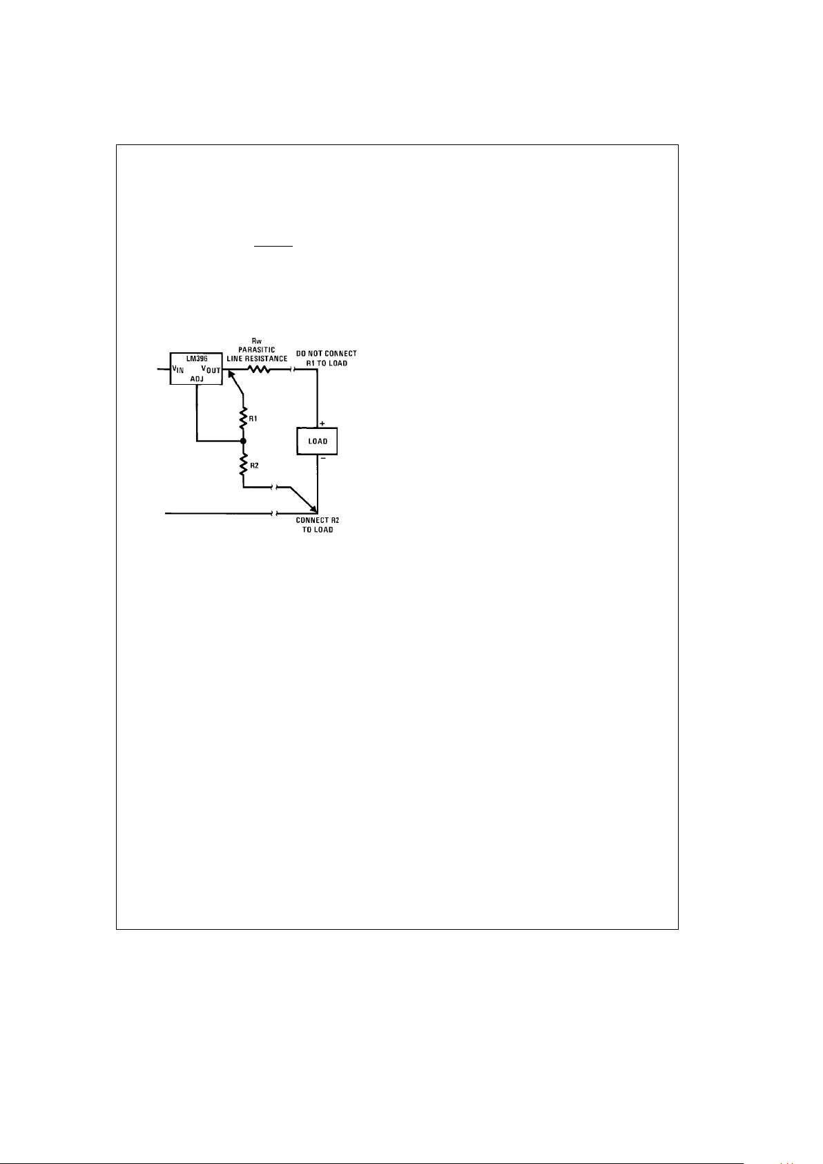
Although it may not be immediately obvious, best load regulation is obtained when the top of the divider is connected
directly
to the output pin,
not to the load
. This is illustrated in
Figure 2
. If R1 were connected to the load, the effective
resistance between the regulator and the load would be
(Rw)
c
#
R2aR1
R1
J
RweLine Resistance
Connected as shown, Rw is not multiplied by the divider
ratio. Rw is about 0.004X per foot using 16 gauge wire. This
translates to 40 mV/ft at 10A load current, so it is important
to keep the positive lead between regulator and load as
short as possible.
TL/H/9059– 2
FIGURE 2. Proper Divider Connection
The input resistance of the sense pin is typically 6 kX, modeled as a resistor between the sense pin and the output pin.
Load regulation will start to degrade if a resistance higher
than 10X is inserted in series with the sense. This assumes
a worst-case condition of 0.5V between output and sense
pins. Lower differential voltage will allow higher sense series
resistance.
Thermal Load Regulation
Thermal, as well as electrical, load regulation must be considered with IC regulators. Electrical load regulation occurs
in microseconds, thermal regulation due to die thermal gradients occurs in the 0.2 ms-20 ms time frame, and regulation due to overall temperature changes in the die occurs
over a 20 ms to 20 minute period, depending on the time
constant of the heat sink used. Gradient induced load regulation is calculated from
DV
OUT
e
(V
IN
b
V
OUT
)c(DI
OUT
)c(b)
beThermal regulation specified on data sheet.
For V
IN
e
9V, V
OUT
e
5V, DI
OUT
e
10A, and b
e
0.005%/W, this yields a 0.2% change in output voltage.
Changes in output voltage due to overall temperature rise
are calculated from
V
OUT
e
(V
IN
b
V
OUT
)c(DI
OUT
)c(TC)c(ijA)
TC
e
Temperature coefficient of output voltage.
i
jA
e
Thermal resistance from junction to ambient. ijAis
approximately 0.5
§
C/Wai of heat sink.
For the same conditions as before, with TC
e
0.003%/§C,
and i
jA
e
1.5§C/W, the change in output voltage will be
0.18%. Because these two thermal terms can have either
polarity, they may subtract from, or add to, electrical load
regulation. For worst-case analysis, they must be assumed
to add. If the output of the regulator is trimmed under load,
only that portion of the load that changes need be used in
the previous calculations, significantly improving output accuracy.
Line Regulation
Electrical line regulation is very good on the LM196Ðtypically less than 0.005% change in output voltage for a 1V
change in input. This level of regulation is achieved only for
very low load currents, however, because of thermal effects. Even with a thermal regulation of 0.002%.W, and a
temperature coefficient of 0.003%/
§
C, DC line regulation
will be dominated by thermal effects as shown by the following example:
Assume V
OUT
e
5V, V
IN
e
9V, I
OUT
e
8A
Following a 10% change in input voltage (0.9), the output
will change quickly (
s
100 ms), due to electrical effects, by
(0.005%V)
c
(0.9V)e0.0045%. In the next 20 ms, the
output will change an additional (0.002%/W)
c
(8A)
c
(0.9V)e0.0144% due to thermal gradients across the die.
After a much longer time, determined by the time constant
of the heat sink, the output will change an additional
(0.003%/
§
C)c(8A)c(0.9V)c(2§C/W)e0.043% due to
the temperature coefficient of output voltage and the thermal resistance from die to ambient. (2
§
C/W was chosen for
this calculation). The sign of these last two terms varies
from part to part, so no assumptions can be made about any
cancelling effects. All three terms must be added for a proper analysis. This yields 0.0045
a
0.0144a0.043
e
0.062% using
typical
values for thermal regulation and temperature coefficient. For worst-case analysis, the maximum
data sheet specifications for thermal regulation and temperature coefficient should be used, along with the
actual
ther-
mal resistance of the heat sink being used.
Paralleling Regulators
Direct paralleling of regulators is not normally recommended because they do not share currents equally. The regulator with the highest reference voltage will supply all the current to the load until it current limits. With an 18A load, for
instance, one regulator might be operating in current limit at
16A while the second device is only carrying 2A. Power dissipation in the high current regulator is extremely high with
attendant high junction temperatures. Long term reliability
cannot be guaranteed under these conditions.
Quasi-paralleling may be accomplished if load regulation is
not critical. The connection shown in
Figure 5a
will typically
share to within 1A, with a worst-case of about 3A. Load
regulation is degraded by 150 mV at 20A loads. An external
op amp may be used as in
Figure 5b
to improve load regula-
tion and provide remote sensing.
5
Page 6

Application Hints (Continued)
Input and Output Capacitors
The LM196 will tolerate a wide range of input and output
capacitance, but long wire runs or small values of output
capacitance can sometimes cause problems. If an output
capacitor is used, it should be 1 mF or larger. We suggest 10
mF solid tantalum if significant improvements in high frequency output impedance are needed (see output impedance graph). This capacitor should be as close to the regulator as possible, with short leads, to reduce the effects of
lead inductance. No input capacitor is needed if the regulator is within 6 inches of the power supply filter capacitor,
using 18 gauge stranded wire. For longer wire runs, the
LM196 input should be bypassed locally with a 4.7 mF (or
larger) solid tantalum capacitor, or a 100 m F (or larger) aluminum electrolytic capacitor.
Correcting for Output Wire Losses (LM196/LM396)
Three-terminal regulators can only provide partial Kelvin
load sensing (see Load Regulation). Full remote sensing
can be added by using an external op amp to cancel the
effect of voltage drops in the unsensed positive output lead.
In
Figure 7
, the LM301A op amp forces the voltage loss
across the unsensed output lead to appear across R3. The
current through R3 then flows out the V
b
pin of the op amp
through R4. The voltage drop across R4 will raise the output
voltage by an amount equal to the line loss, just cancelling
the line loss itself. A small (j40 mV) initial output voltage
error is created by the quiescent current of the op amp.
Cancellation range is limited by the maximum output current
of the op amp, about 300 mV as shown. This can be raised
by increasing R3 or R4 at the expense of more initial output
error.
Transformers and Diodes
Proper transformer ratings are very important in a high current supply because of the conflicting requirements of efficiency and tolerance to low-line conditions. A transformer
with a high secondary voltage will waste power and cause
unnecessary heating in the regulator. Too low a secondary
voltage will cause loss of regulation under low-line conditions. The following formulas may be used to calculate the
required secondary voltage and current ratings using a fullwave center tap:
V
rms
e
#
V
OUT
a
V
REG
a
V
RECT
a
V
RIPPLE
0
2
J
#
V
NOM
V
LOW
J#
(1.1)
*
J
I
rms
e
(I
OUT
) (1.2) (Full-wave center tap)
where:
V
OUT
e
DC regulated output voltage
V
REG
e
Minimum input-output voltage of regulator
V
RECT
e
Rectifier forward voltage drop at three times DC
output current
V
RIPPLE
e
1/2 peak-to-peak capacitor ripple voltage
e
(5.3c10
b
3
)(I
OUT
)
2C
*The factor of 1.1 is only an approximate factor accounting for load regulation of the transformer.
V
NOM
e
Nominal line voltage AC rms
V
LOW
e
Low line voltage AC rms
I
OUT
e
DC output current
Example: I
OUT
e
10A, V
OUT
e
5V
Assume: V
REG
e
2.2V, V
RECT
e
1.2V
V
RIPPLE
e
2 Vp-p, V
NOM
e
115V,
V
LOW
e
105V
V
rms
e
#
5a2.2a1.2a1
0
2
J#
115
105
J
1.1
e
8.01 V
rms
Capacitor C
e
(5.3c10
b
3
)(I
OUT
)
2cV
RIPPLE
e
(5.3c10
b
3
)(10)
2
e
26,500 mF
The diodes used in a full-wave rectified capacitor input supply must have a DC current rating considerably higher than
the average current flowing through them. In a 10A supply,
for instance, the average current through each diode is only
5A, but the diodes should have a rating of 10A – 15A. There
are many reasons for this, both thermal and electrical. The
diodes conduct current in pulses about 3.5 ms wide with a
peak value of 5 –8 times the average value, and an rms
value 1.5– 2.0 times the average value. This results in long
term diode heating roughly equivalent to 10A DC current.
The most demanding condition however, may be the one
cycle surge through the diode during power turn on. The
peak value of the surge is about 10 – 20 times the DC output
current of the supply, or 100A – 200A for a 10A supply. The
diodes must have a one cycle non-repetitive surge rating of
200A or more, and this is usually not found in a diode with
less than 10A average current rating. Keep in mind that
even though the LM196 may be used at current levels below 10A, the diodes may still have to survive shorted output
conditions where average current could rise to 12A – 15A.
Smaller transformers and filter capacitors used in lower current supplies will reduce surge currents, but unless specific
information is available on worst-case surges, it is best not
to economize on diodes. Stud-mounted devices in a DO-4
package are recommended. Cathode-to-case types may be
bolted directly to the same heat sink as the LM196 because
the case of the regulator is its power input. Part numbers to
consider are the 1N1200 series rated at 12A average current in a DO-4 stud package. Additional types include common cathode duals in a TO-3 package, both standard and
Schottky, and various duals in plastic filled assemblies.
Schottky diodes will improve efficiency, especially in low
voltage applications. In a 5V supply for instance, Schottky
diodes will decrease wasted power by up to 6W, or alternatively provide an additional 5% ‘‘drop out’’ margin for lowline conditions. Several manufacturers are producing ‘‘high
efficiency’’ diodes with a forward voltage drop nearly as
good as Schottkys at high current levels. These devices do
not have the low breakdown voltages of Schottkys, so are
much less prone to reverse breakdown induced failures.
6
Page 7

Typical Performance Characteristics
Reference Drift Differential*
Minimum Input-Output
Differential*
Minimum Input-Output
TL/H/9059– 3
*VINis reduced until output drops 2% *VINis reduced until output drops 2%
Current Limit Dissipation*
Maximum Power
Thermal Resistance*
Maximum Heat Sink
TL/H/9059– 4
*As limited by maximum junction temperature. *See ‘‘Heat Sinking’’ under Applications Hints.
Thermal Resistance*
Maximum Heat Sink
Joint Compound
Resistance Using Thermal
TO-3 Interface Thermal
Thermal Regulation
TL/H/9059– 5
*See ‘‘Heat Sinking’’ under Application Hints.
7
Page 8

Typical Performance Characteristics (Continued)
Reference Voltage Noise* Ripple Rejection Ripple Rejection
TL/H/9059– 6
*To obtain output noise, multiply by
V
OUT
/1.25 if adjustment pinis not bypassed.
Adjustment Current (Ce25 mF)
Adjustment Pin Bypassed
Output Impedance
Output Impedance*
TL/H/9059– 7
*For output voltages other than 5V, multiply ver-
tical scale readings by V
OUT
/5.
Adjustment Pin Bypassed
Line Transient Response
Adjustment Pin Bypassed
Load Transient Response
Line Transient Response*
TL/H/9059– 8
*With no adjustment pin bypass. For output volt-
ages other than 5V, multiply vertical scale by
V
OUT
/5.
8
Page 9

Typical Performance Characteristics (Continued)
Load Transient Response*
TL/H/9059– 9
*With no adjustment pin bypass. For output volt-
ages other than 5V, multiply vertical scale by
V
OUT
/5.
Typical Applications (Continued)
TL/H/9059– 10
*Regulation can be improved by adding an LM336 reference diode to increase the effective reference
voltage to 3.75V. Load and line regulation are improved by 3:1, including thermal effects.
FIGURE 3. Improving Regulation*
TL/H/9059– 11
*R3 is selected to supply partial load current. Therefore, a minimum load
must always be maintained to prevent the regulated output from rising uncontrolled. R3 must be greater than (V
MAX
b
V
OUT
)/I
MIN
, where V
MAX
is
worst-case high input voltage, and I
MIN
is the minimum load current. R3
must be rated for at least (V
IN
b
V
OUT
)2/R3 watts. Regulator power dissipation will be reduced by a factor of 2 –3 in a typical situation where minimum
load current is 1/2 full load current. Regulator dissipation will peak at:
V
IN
e
(R3)(I
OUT
)
2
a
V
OUT
and will be equal to:
P
MAX
e
(R3)(I
OUT
)
2
4
Assuming: (R3)(I
OUT
)sV
MAX
b
V
OUT
A few words of caution; (1) R3 power rating must be increased to (V
MAX
)2/
R3 if continuous output shorts are possible. (2) Under normal load conditions, system power dissipation is not changed, but under short circuit conditions
system
power dissipation increases by (VIN)2/R3 watts over the already high power of a shorted regulator. The LM196 will not be harmed and
neither will R3 if it is rated properly, but the raw supply components must be
able to withstand the overload also. Thermal shutdown of the LM196 will
probably occur for sustained shorts, somewhat alleviating the problem.
FIGURE 4. Reducing Regulator Power Dissipation
9
Page 10

Typical Applications (Continued)
TL/H/9059– 12
FIGURE 5a. Paralleling Regulators
TL/H/9059– 13
*2 feet ofÝ18 CU wire
**Total voltage drop across output wire and connector should not exceed 0.3V
FIGURE 5b
TL/H/9059– 14
Output will be withing20 mV at 25§C, no load. Regulation of tracking units is improved by V
OUT
/1.25 compared to a normal connection.
Regulation of master unit is unchanged. Load or input voltage changes on slave units do not affect other units, but all units will be affected
by changes on master. A short on any output will cause all other outputs to drop to approximately 2V.
FIGURE 6. Tracking Regulators
10
Page 11

Typical Applications (Continued)
TL/H/9059– 15
*Parasatic line resistance created by wiring
connectors, or parallel ballasting.
FIGURE 7. Correcting for Line Losses
TL/H/9059– 16
Power NPNs have low collecter resistance, and do not require collector bond wires. Collectors are all common to substrate.
Standard NPNs are still isolated.
FIGURE 8. Process Technology
Connection Diagram
Metal Can Package
TL/H/9059– 18
Bottom View
Order Number LM196K STEEL or LM396K STEEL
See NS Package Number K02B
11
Page 12

Schematic Diagram*
TL/H/9059– 17
*Drive is tied to V
IN
and sense is tied to V
OUT
on LM196 and LM396.
12
Page 13

13
Page 14

LM196/LM396 10 Amp Adjustable Voltage Regulator
Physical Dimensions inches (millimeters)
TO-3 Metal Can Package (K)
Order Number LM196K STEEL
or LM396K STEEL
NS Package Number K02B
LIFE SUPPORT POLICY
NATIONAL’S PRODUCTS ARE NOT AUTHORIZED FOR USE AS CRITICAL COMPONENTS IN LIFE SUPPORT
DEVICES OR SYSTEMS WITHOUT THE EXPRESS WRITTEN APPROVAL OF THE PRESIDENT OF NATIONAL
SEMICONDUCTOR CORPORATION. As used herein:
1. Life support devices or systems are devices or 2. A critical component is any component of a life
systems which, (a) are intended for surgical implant support device or system whose failure to perform can
into the body, or (b) support or sustain life, and whose be reasonably expected to cause the failure of the life
failure to perform, when properly used in accordance support device or system, or to affect its safety or
with instructions for use provided in the labeling, can effectiveness.
be reasonably expected to result in a significant injury
to the user.
National Semiconductor National Semiconductor National Semiconductor National Semiconductor
Corporation Europe Hong Kong Ltd. Japan Ltd.
1111 West Bardin Road Fax: (
a
49) 0-180-530 85 86 13th Floor, Straight Block, Tel: 81-043-299-2309
Arlington, TX 76017 Email: cnjwge@tevm2.nsc.com Ocean Centre, 5 Canton Rd. Fax: 81-043-299-2408
Tel: 1(800) 272-9959 Deutsch Tel: (
a
49) 0-180-530 85 85 Tsimshatsui, Kowloon
Fax: 1(800) 737-7018 English Tel: (
a
49) 0-180-532 78 32 Hong Kong
Fran3ais Tel: (
a
49) 0-180-532 93 58 Tel: (852) 2737-1600
Italiano Tel: (
a
49) 0-180-534 16 80 Fax: (852) 2736-9960
National does not assume any responsibility for use of any circuitry described, no circuit patent licenses are implied and National reserves the right at any time without notice to change said circuitry and specifications.
 Loading...