

Page 1
LM194/LM394 Supermatch Pair
General Description
The LM194 and LM394 are junction isolated ultra wellmatched monolithic NPN transistor pairs with an order of
magnitude improvement in matching over conventional transistor pairs. This was accomplished by advanced linear processing and a unique new device structure.
Electrical characteristics of these devices such as drift versus initial offset voltage, noise, and the exponential relationship of base-emitter voltage to collector current closely approach those of a theoretical transistor. Extrinsic emitter
and base resistances are much lower than presently available pairs, either monolithic or discrete, giving extremely low
noise and theoretical operation over a wide current range.
Most parameters are guaranteed over a current range of
1 mA to 1 mA and 0V up to 40V collector-base voltage,
ensuring superior performance in nearly all applications.
To guarantee long term stability of matching parameters,
internal clamp diodes have been added across the emitterbase junction of each transistor. These prevent degradation
due to reverse biased emitter currentÐthe most common
cause of field failures in matched devices. The parasitic isolation junction formed by the diodes also clamps the substrate region to the most negative emitter to ensure complete isolation between devices.
The LM194 and LM394 will provide a considerable improvement in performance in most applications requiring a closely
matched transistor pair. In many cases, trimming can be
eliminated entirely, improving reliability and decreasing
costs. Additionally, the low noise and high gain make this
device attractive even where matching is not critical.
The LM194 and LM394/LM394B/LM394C are available in
an isolated header 6-lead TO-5 metal can package. The
LM394/LM394B/LM394C are available in an 8-pin plastic
dual-in-line package. The LM194 is identical to the LM394
except for tighter electrical specifications and wider temperature range.
Features
Y
Y
Y
Y
Y
Y
Y
Y
LM194/LM394 Supermatch Pair
December 1994
Emitter-base voltage matched to 50 mV
Offset voltage drift less than 0.1 mV/§C
Current gain (hFE) matched to 2%
Common-mode rejection ratio greater than 120 dB
Parameters guaranteed over 1 mA to 1 mA collector
current
Extremely low noise
Superior logging characteristics compared to
conventional pairs
Plug-in replacement for presently available devices
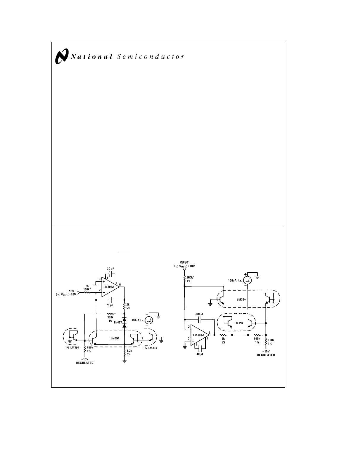
Typical Applications
Low Cost Accurate Square Root Circuit
I
OUT
C
1995 National Semiconductor Corporation RRD-B30M115/Printed in U. S. A.
b
5
e
10
.010 V
IN
TL/H/9241– 1
*Trim for full scale accuracy
TL/H/9241
Low Cost Accurate Squaring Circuit
I
OUT
b
6
(VIN)
2
e
10
TL/H/9241– 2
Page 2
Absolute Maximum Ratings
If Military/Aerospace specified devices are required,
please contact the National Semiconductor Sales
Office/Distributors for availability and specifications.
(Note 4)
Collector Current 20 mA
Collector-Emitter Voltage V
Collector-Emitter Voltage 35V
LM394C 20V
Collector-Base Voltage 35V
LM394C 20V
Collector-Substrate Voltage 35V
LM394C 20V
Collector-Collector Voltage 35V
LM394C 20V
MAX
Base-Emitter Current
g
10 mA
Power Dissipation 500 mW
Junction Temperature
LM194
LM394/LM394B/LM394C
Storage Temperature Range
b
55§Ctoa125§C
b
25§Ctoa85§C
b
65§Ctoa150§C
Soldering Information
Metal Can Package (10 sec.) 260
Dual-In-Line Package (10 sec.) 260
Small Outline Package
Vapor Phase (60 sec.) 215
Infrared (15 sec.) 220
See AN-450 ‘‘Surface Mounting and their Effects on Product Reliability’’ for other methods of soldering surface
mount devices.
C
§
C
§
C
§
C
§
Electrical Characteristics (T
Parameter Conditions
e
25§C)
J
LM194 LM394 LM394B/394C
Units
Min Typ Max Min Typ Max Min Typ Max
Current Gain (hFE)V
Current Gain Match, V
(hFEMatch) I
][
e
100[DI
h
B
FE(MIN)
I
C
Emitter-Base Offset V
Voltage I
e
0V to V
CB
e
I
1 mA 350 700 300 700 225 500
C
e
I
100 mA 350 550 250 550 200 400
C
e
I
10 mA 300 450 200 450 150 300
C
e
I
1 mA 200 300 150 300 100 200
C
e
0V to V
CB
e
10 mA to 1 mA 0.5 2 0.5 4 1.0 5 %
C
]
e
I
1 mA 1.0 1.0 2.0 %
C
e
0
CB
e
1 mAto1mA
C
MAX
MAX
(Note 1)
25 100 25 150 50 200 mV
Change in Emitter-Base (Note 1)
Offset Voltage vs I
Collector-Base Voltage V
(CMRR)
Change in Emitter-Base V
Offset Voltage vs I
Collector Current
Emitter-Base Offset I
Voltage Temperature I
Drift VOSTrimmed to 0 at 25§C 0.03 0.1 0.03 0.3 0.03 0.5 mV/§C
Logging Conformity I
Collector-Base Leakage V
Collector-Collector V
Leakage
Input Voltage Noise I
Collector to Emitter I
Saturation Voltage I
Note 1: Collector-base voltage is swept from 0 to V
Note 2: Offset voltage drift with V
within 0.003% over the entire temperature range. Measurements taken at
Note 3: Logging conformity is measured by computing the best fit to a true exponential and expressing the error as a base-emitter voltage deviation.
Note 4: Refer to RETS194X drawing of military LM194H version for specifications.
e
1 mAto1mA,
C
e
0V to V
CB
e
CB
e
C
e
C
e
C1
e
C
e
V
CB
e
CB
e
CC
e
C
e
100 Hz to 100 kHz
f
e
C
e
C
e
OS
MAX
0V,
1 mA to 0.3 mA
10 mA to 1 mA (Note 2)
I
C2
3nAto300mA,
0, (Note 3)
V
MAX
V
MAX
100 mA, V
e
1 mA, I
B
e
1 mA, I
B
e
0atT
25§C is valid only when the ratio of IC1to IC2is adjusted to give the initial zero offset. This ratio must be held to
A
10 25 10 50 10 100 mV
525 550 550 mV
0.08 0.3 0.08 1.0 0.2 1.5 mV/
150 150 150 mV
0.05 0.25 0.05 0.5 0.05 0.5 nA
0.1 2.0 0.1 5.0 0.1 5.0 nA
e
0V,
CB
1.8 1.8 1.8 nV/
10 mA 0.2 0.2 0.2 V
100 mA 0.1 0.1 0.1 V
at a collector current of 1 mA, 10 mA, 100 mA, and 1 mA.
MAX
a
25§C and temperature extremes.
0
§
Hz
C
2
Page 3
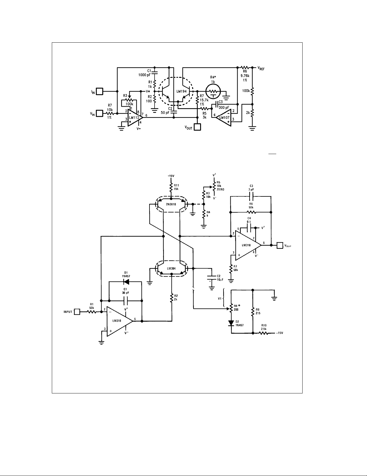
Typical Applications (Continued)
Fast, Accurate Logging Amplifier, V
e
10V to 0.1 mV or I
IN
e
1mAto10nA
IN
Voltage Controlled Variable Gain Amplifier
*1kX(g1%) at 25§C,a3500 ppm/§C.
Available from Vishay Ultronix,
Grand Junction, CO, Q81 Series.
eb
V
OUT
TL/H/9241– 3
V
IN
log
10
V
#
J
REF
*R8– R10 and D2 provide a temperature Distortionk0.1%
independent gain control. Bandwidth
eb
336 V1 (dB) 100 dB gain range
G
l
1 MHz
3
TL/H/9241– 4
Page 4

Typical Applications (Continued)
Precision Low Drift Operational Amplifier
Common-mode range 10V
I
25 nA
BIAS
I
0.5 nA
OS
V
(untrimmed) 125 mV
OS
(DV
/DT) 0.2 mV/C
OS
CMRR 120 dB
A
2,500,000
VOL
*C 200 pF for unity gain
C 30 pF for A
C 5 pF for A
C 0 pF for AV1000
10
V
100
V
TL/H/9241– 5
High Accuracy One Quadrant Multiplier/Divider
(X) (Y)
e
V
OUT
*Typical linearity 0.1%
; positive inputs only.
(Z)
4
TL/H/9241– 6
Page 5

Typical Applications (Continued)
High Performance Instrumentation Amplifier
6
10
e
*Gain
R
S
Performance Characteristics
Ge10,000 Ge1,000 Ge100 Ge10
g
Linearity of Gain (
10V Output)
Common-Mode Rejection Ratio (60 Hz)
Common-Mode Rejection Ratio (1 kHz)
Power Supply Rejection Ratio
a
Supply
b
Supply
b
Bandwidth (
3 dB) 50 50 50 50 kHz
Slew Rate 0.3 0.3 0.3 0.3 V/ms
Offset Voltage Drift**
Common-Mode Input Resistance
Differential Input Resistance
Input Referred Noise (100 Hz
sfs
10 kHz) 5 6 12 70
s
t
t
l
l
s
l
l
3x10
Input Bias Current 75 75 75 75 nA
0.01
120
110
110
110
0.25
10
s
0.01s0.02s0.05 %
t
120t110t90 dB
t
l
l
s
9
l
8
l
3x10
t
110
110l110l110 dB
l
110
0.4 2
9
l
10
8
l
3x10
90
90
10
9
8
l
t
70 dB
l
70 dB
s
10 mV/§C
l
109X
3x108X
nV
Hz
0
Input Offset Current 1.5 1.5 1.5 1.5 nA
Common-Mode Range
Output Swing (R
**Assumess5 ppm/§C tracking of resistors
e
10 kX)
L
g
g
g
11
g
13
g
11
13
g
11
g
10 V
g
13
13 V
5
TL/H/9241– 7
Page 6

Typical Performance Characteristics
Small Signal Current Gain vs
Collector Current DC Current Gain vs Temperature
Offset Voltage Drift vs Initial
Offset Voltage
Small Signal Output Conductance
vs Collector Current
Base-Emitter On Voltage vs
Collector Current
Collector-Emitter
Saturation Voltage
vs Collector Current
Unity Gain Frequency (ft)vs
Collector Current
Small Signal Input
Resistance (h
vs Collector Current
Input Voltage Noise vs
Frequency
)
ie
Base Current Noise
vs Frequency
Noise Figure vs
Collector Current
6
Collector to Collector
Capacitance vs Reverse
Bias Voltage
TL/H/9241– 8
Page 7

Typical Performance Characteristics (Continued)
Collector to Collector Capacitance
vs Collector-Substrate Voltage
Collector-Base Leakage vs
Temperature
Emitter-Base Capacitance vs
Reverse Bias Voltage
Collector to Collector Leakage
vs Temperature
Emitter-Base Log Conformity
Collector-Base Capacitance vs
Reverse Bias Voltage
Offset Voltage Long Term
Stability at High Temperature
TL/H/9241– 9
TL/H/9241– 10
Low Frequency Noise of Differential Pair*
*Unit must be in still air environment so that differential
lead temperature is held to less than 0.0003
C.
§
7
TL/H/9241– 11
Page 8

Connection Diagrams
Metal Can Package
Top View
Order Number LM194H/883*,
LM394H, LM394BH or LM394CH
See NS Package Number H06C
TL/H/9241– 12
Dual-In-Line and Small Outline Packages
TL/H/9241– 13
Top View
Order Number LM394N or LM394CN
See NS Package Number N08E
*Available per SMDÝ5962-8777701
8
Page 9

Physical Dimensions inches (millimeters)
Order Number LM194H/883, LM394H, LM394BH or LM394CH
Metal Can Package (H)
NS Package Number H06C
9
Page 10

Physical Dimensions inches (millimeters) (Continued)
LM194/LM394 Supermatch Pair
Molded Dual-In-Line Package (N)
Order Number LM394CN or LM394N
NS Package Number N08E
LIFE SUPPORT POLICY
NATIONAL’S PRODUCTS ARE NOT AUTHORIZED FOR USE AS CRITICAL COMPONENTS IN LIFE SUPPORT
DEVICES OR SYSTEMS WITHOUT THE EXPRESS WRITTEN APPROVAL OF THE PRESIDENT OF NATIONAL
SEMICONDUCTOR CORPORATION. As used herein:
1. Life support devices or systems are devices or 2. A critical component is any component of a life
systems which, (a) are intended for surgical implant support device or system whose failure to perform can
into the body, or (b) support or sustain life, and whose be reasonably expected to cause the failure of the life
failure to perform, when properly used in accordance support device or system, or to affect its safety or
with instructions for use provided in the labeling, can effectiveness.
be reasonably expected to result in a significant injury
to the user.
National Semiconductor National Semiconductor National Semiconductor National Semiconductor
Corporation Europe Hong Kong Ltd. Japan Ltd.
1111 West Bardin Road Fax: (
Arlington, TX 76017 Email: cnjwge@tevm2.nsc.com Ocean Centre, 5 Canton Rd. Fax: 81-043-299-2408
Tel: 1(800) 272-9959 Deutsch Tel: (
Fax: 1(800) 737-7018 English Tel: (
National does not assume any responsibility for use of any circuitry described, no circuit patent licenses are implied and National reserves the right at any time without notice to change said circuitry and specifications.
Fran3ais Tel: (
Italiano Tel: (
a
49) 0-180-530 85 86 13th Floor, Straight Block, Tel: 81-043-299-2309
a
49) 0-180-530 85 85 Tsimshatsui, Kowloon
a
49) 0-180-532 78 32 Hong Kong
a
49) 0-180-532 93 58 Tel: (852) 2737-1600
a
49) 0-180-534 16 80 Fax: (852) 2736-9960
 Loading...