

Page 1
LM3940
1A Low Dropout Regulator for 5V to 3.3V Conversion
General Description
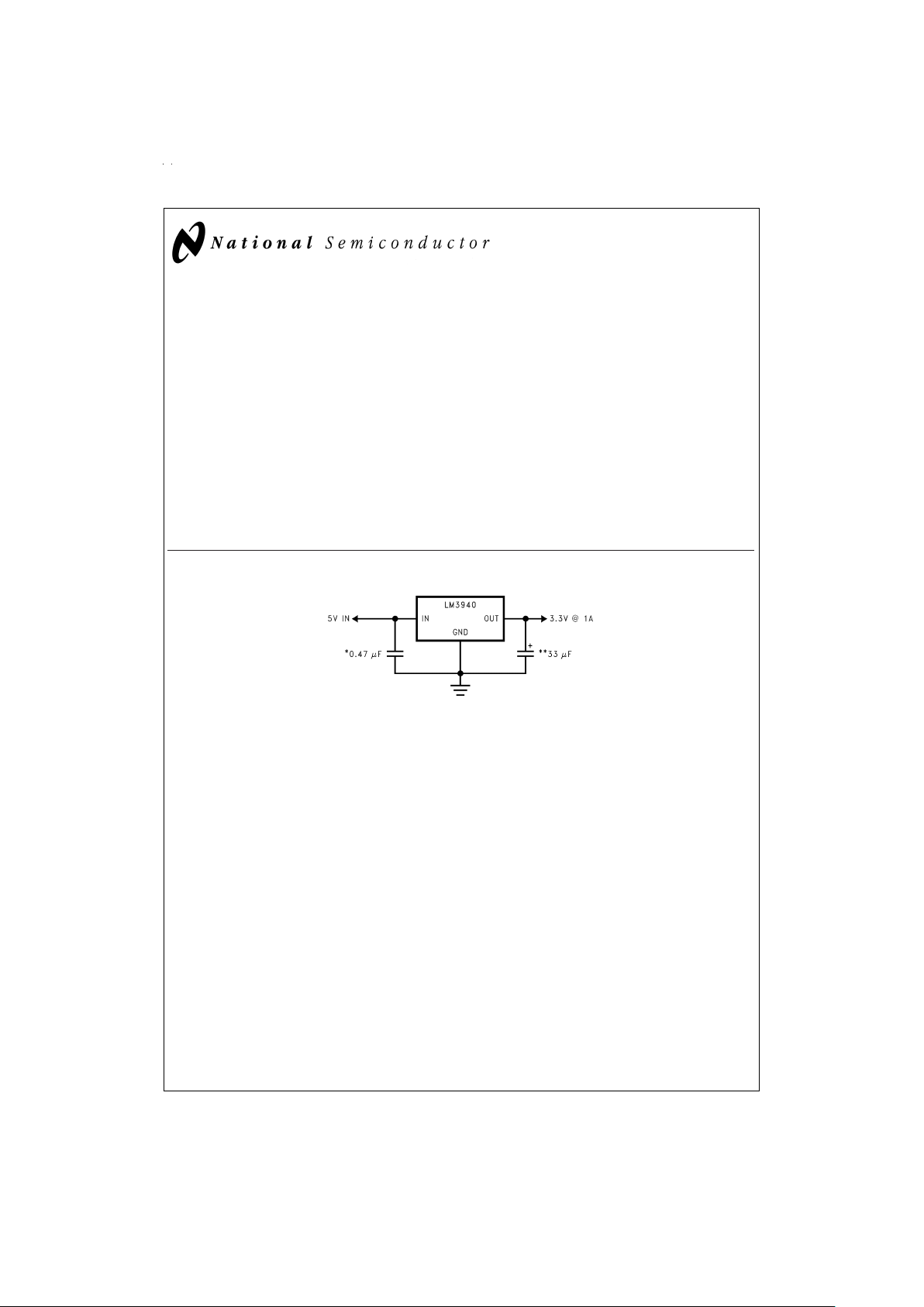
The LM3940 is a 1A low dropout regulator designed to provide 3.3V from a 5V supply.
The LM3940 is ideally suited for systems which contain both
5V and 3.3V logic, with prime power provided from a 5V bus.
Because the LM3940 is a true low dropout regulator, it can
hold its 3.3V output in regulation with input voltages as low
as 4.5V.
The T0-220 package of the LM3940 means that in most applications the full 1A of load current can be delivered without
using an additional heatsink.
The surface mount TO-263 package uses minimum board
space, and gives excellent power dissipation capability when
soldered to a copper plane on the PC board.
Features
n Output voltage specified over temperature
n Excellent load regulation
n Guaranteed 1A output current
n Requires only one external component
n Built-in protection against excess temperature
n Short circuit protected
Applications
n Laptop/Desktop Computers
n Logic Systems
Typical Application
DS012080-1
*
Required if regulator is located more than 1" from the power supply filter capacitor or if battery power is used.
**
See Application Hints.
May 1999
LM3940 1A Low Dropout Regulator for 5V to 3.3V Conversion
© 1999 National Semiconductor Corporation DS012080 www.national.com
Page 2
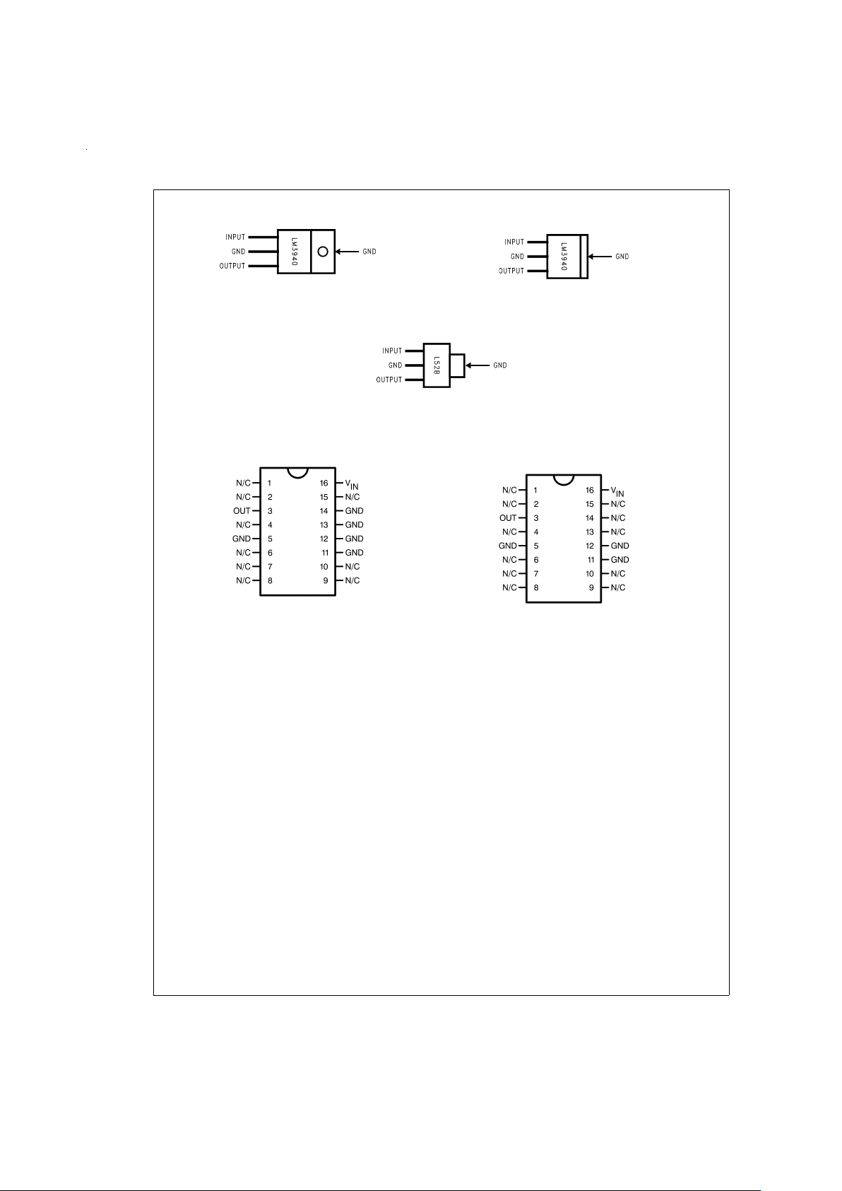
Connection Diagram/Ordering Information
DS012080-2
3-Lead TO-220 Package
(Front View)
Order Part Number LM3940IT-3.3
NSC Drawing Number TO3B
DS012080-3
3-Lead TO-263 Package
(Front View)
Order Part Number LM3940IS-3.3
NSC Drawing Number TS3B
DS012080-10
3-Lead SOT-223
(Front View)
Order Part Number LM3940IMP-3.3
Package Marked L52B
NSC Drawing Number MA04A
DS012080-27
16-Lead Ceramic Dual-in-Line Package
(Top View)
Order Part Number LM3940J-3.3-QML
5962-9688401QEA
NSC Drawing Number J16A
DS012080-28
16-Lead Ceramic Surface-Mount Package
(Top View)
Order Part Number LM3940WG-3.3-QML
5962-9688401QXA
NSC Drawing Number WG16A
www.national.com 2
Page 3
Absolute Maximum Ratings (Note 1)
If Military/Aerospace specified devices are required,
please contact the National Semiconductor Sales Office/
Distributors for availability and specifications.
Storage Temperature Range −65˚C to +150˚C
Operating Junction Temperature Range −40˚C to +125˚C
Lead Temperature (Soldering, 5 seconds) 260˚C
Power Dissipation (Note 2) Internally Limited
Input Supply Voltage 7.5V
ESD Rating (Note 3) 2 kV
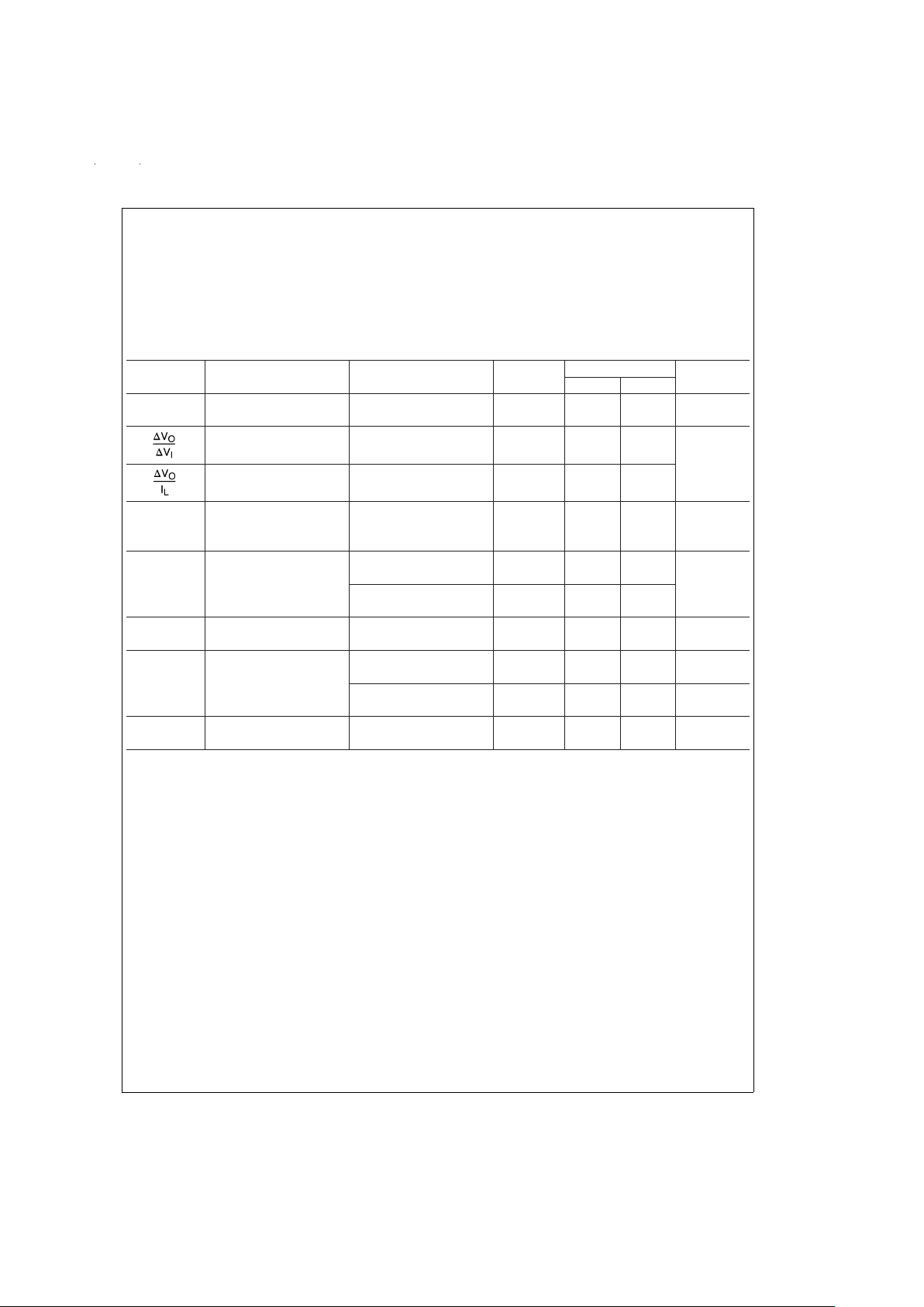
Electrical Characteristics
Limits in standard typeface are for T
J
=
25˚C, and limits in boldface type apply over the full operating temperature range. Un-
less otherwise specified: V
IN
=
5V, I
L
=
1A, C
OUT
=
33 µF.
Symbol Parameter Conditions Typical LM3940 (Note 4) Units
min max
V
O
Output Voltage 5 mA ≤ IL≤ 1A 3.3 3.20 3.40 V
3.13 3.47
Line Regulation I
L
=
5mA
20
40 mV
4.5V ≤ V
O
≤ 5.5V
Load Regulation 50 mA ≤ IL≤ 1A
35
50
80
Z
O
Output Impedance IL(DC)=100 mA
I
L
(AC)=20 mA (rms) 35 mΩ
f=120 Hz
I
Q
Quiescent Current 4.5V ≤ VIN≤ 5.5V 10 15 mA
I
L
=
5mA 20
V
IN
=
5V 110 200
I
L
=
1A 250
e
n
Output Noise Voltage BW=10 Hz–100 kHz 150 µV (rms)
I
L
=
5mA
V
O−VIN
Dropout Voltage I
L
=
1A 0.5 0.8 V
(Note 5) 1.0
I
L
=
100 mA 110 150 mV
200
I
L
(SC) Short Circuit Current R
L
=
0 1.7 1.2 A
Note 1: Absolute maximum ratings indicate limits beyond which damage to the component may occur. Electrical specifications do not apply when operating the device outside of its rated operating conditions.
Note 2: The maximum allowable power dissipation is a function of the maximum junction temperature, T
J
, the junction-to-ambient thermal resistance, θ
J−A
, and the
ambient temperature,T
A
. Exceeding themaximumallowablepower dissipation will cause excessive die temperature, and the regulator will go into thermal shutdown.
The value of θ
J−A
(for devices in still air with no heatsink) is 60˚C/W for the TO-220 package, 80˚C/W for the TO-263 package, and 174˚C/W for the SOT-223 package.
The effective value of θ
J−A
can be reduced by using a heatsink (see Application Hints for specific information on heatsinking).
Note 3: ESD rating is based on the human body model: 100 pF discharged through 1.5 kΩ.
Note 4: All limits guaranteed for T
J
=
25˚C are 100%tested and are used to calculate Outgoing Quality Levels. All limits at temperature extremes are guaranteed
via correlation using standard Statistical Quality Control (SQC) methods.
Note 5: Dropout voltage is defined as the input-output differential voltage where the regulator output drops to a value that is 100 mV below the value that is measured
at V
IN
=
5V.
www.national.com3
Page 4
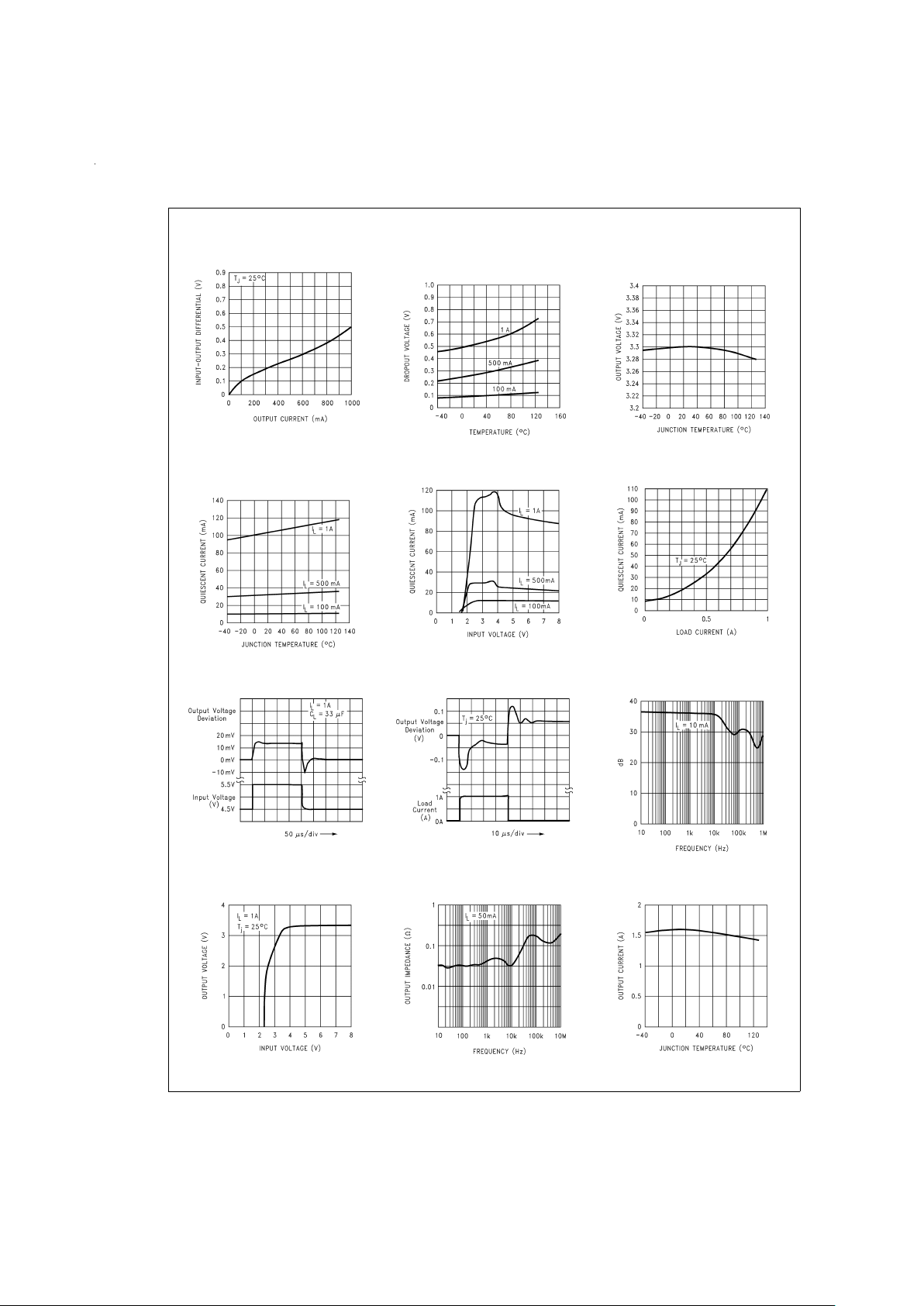
Typical Performance Characteristics
Dropout Voltage
DS012080-13
Dropout Voltage
vs Temperature
DS012080-14
Output Voltage
vs Temperature
DS012080-15
Quiescent Current
vs Temperature
DS012080-16
Quiescent Current vs V
IN
DS012080-17
Quiescent Current vs Load
DS012080-18
Line Transient Response
DS012080-19
Load Transient Response
DS012080-20
Ripple Rejection
DS012080-21
Low Voltage Behavior
DS012080-22
Output Impedance
DS012080-23
Peak Output Current
DS012080-24
www.national.com 4
Page 5

Application Hints
EXTERNAL CAPACITORS
The output capacitor is critical to maintaining regulator stability, and must meet the required conditions for both ESR
(Equivalent Series Resistance) and minimum amount of capacitance.
MINIMUM CAPACITANCE:
The minimum output capacitance required to maintain stabil-
ity is 33 µF (this value may be increased without limit).
Larger values of output capacitance will give improved transient response.
ESR LIMITS:
The ESR of the output capacitor will cause loop instability if
it is too high or too low.The acceptable range of ESR plotted
versus load current is shown in the graph below.
It is essential that the output capacitor meet these requirements,
or oscillations can result.
It is important to note that for most capacitors, ESR is specified only at room temperature. However, the designer must
ensure that the ESR will stay inside the limits shown over the
entire operating temperature range for the design.
For aluminum electrolytic capacitors, ESR will increase by
about 30X as the temperature is reduced from 25˚C to
−40˚C. This type of capacitor is not well-suited for low temperature operation.
Solid tantalum capacitors have a more stable ESR over temperature, but are more expensive than aluminum electrolytics. A cost-effective approach sometimes used is to parallel
an aluminum electrolytic with a solid Tantalum, with the total
capacitance split about 75/25%with the Aluminum being the
larger value.
If two capacitors are paralleled, the effective ESR is the parallel of the two individual values. The “flatter” ESR of the Tantalum will keep the effective ESR from rising as quickly at low
temperatures.
HEATSINKING
A heatsink may be required depending on the maximum
power dissipation and maximum ambient temperature of the
application. Under all possible operating conditions, the junction temperature must be within the range specified under
Absolute Maximum Ratings.
To determine if a heatsink is required, the power dissipated
by the regulator, P
D
, must be calculated.
The figure below shows the voltages and currents which are
present in the circuit, as well as the formula for calculating
the power dissipated in the regulator:
The next parameter which must be calculated is the maximum allowable temperature rise, T
R
(max). This is calcu-
lated by using the formula:
T
R
(max)=TJ(max) − TA(max)
Where: T
J
(max) is the maximum allowable junction tem-
perature, which is 125˚C for commercial
grade parts.
T
A
(max) is the maximum ambient temperature
which will be encountered in the application.
Using the calculated values for T
R
(max) and PD, the maximum allowable value for the junction-to-ambient thermal resistance, θ
(J−A)
, can now be found:
θ
(J−A)
=
T
R
(max)/P
D
IMPORTANT: If the maximum allowable value for θ
(J−A)
is
found to be ≥ 60˚C/W for the TO-220 package, ≥ 80˚C/W for
the TO-263 package, or ≥174˚C/W for the SOT-223 package, no heatsink is needed since the package alone will dissipate enough heat to satisfy these requirements.
If the calculated value for θ
(J−A)
falls below these limits, a
heatsink is required.
HEATSINKING TO-220 PACKAGE PARTS
The TO-220 can be attached to a typical heatsink, or secured to a copper plane on a PC board. If a copper plane is
to be used, the values of θ
(J−A)
will be the same as shown in
the next section for the TO-263.
DS012080-5
FIGURE 1. ESR Limits
DS012080-6
I
IN
=
I
L+IG
P
D
=
(V
IN−VOUT)IL
+(VIN)I
G
FIGURE 2. Power Dissipation Diagram
www.national.com5
Page 6

Application Hints (Continued)
If a manufactured heatsink is to be selected, the value of
heatsink-to-ambient thermal resistance, θ
(H−A)
, must first be
calculated:
θ
(H−A)
=
θ
(J−A)
− θ
(C−H)
− θ
(J−C)
Where: θ
(J−C)
is defined as the thermal resistance from
the junction to the surface of the case. A
value of 4˚C/W can be assumed for θ
(J−C)
for this calculation.
θ
(C−H)
is defined as the thermal resistance between the case and the surface of the heatsink. The value of θ
(C−H)
will vary from
about 1.5˚C/W to about 2.5˚C/W (depending on method of attachment, insulator,
etc.). If the exact value is unknown, 2˚C/W
should be assumed for θ
(C−H)
.
When a value for θ
(H−A)
is found using the equation shown,
a heatsink must be selected that has a value that is less than
or equal to this number.
θ
(H−A)
is specified numerically by the heatsink manufacturer
in the catalog, or shown in a curve that plots temperature rise
vs power dissipation for the heatsink.
HEATSINKING TO-263 AND SOT-223 PACKAGE PARTS
Both the TO-263 (“S”) and SOT-223 (“MP”) packages use a
copper plane on the PCB and the PCB itself as a heatsink.
To optimize the heat sinking ability of the plane and PCB,
solder the tab of the package to the plane.
Figure 3
shows for the TO-263 the measured values of θ
(J−A)
for different copper area sizes using a typical PCB with 1
ounce copper
and no solder mask over the copper area used
for heatsinking.
As shown in the figure, increasing the copper area beyond 1
square inch produces very little improvement. It should also
be observed that the minimum value of θ
(J−A)
for the TO-263
package mounted to a PCB is 32˚C/W.
As a design aid,
Figure 4
shows the maximum allowable
power dissipation compared to ambient temperature for the
TO-263 device (assuming θ
(J−A)
is 35˚C/W and the maxi-
mum junction temperature is 125˚C).
Figure 5
and
Figure 6
show the information for the SOT-223
package.
Figure 6
assumes a θ
(J−A)
of 74˚C/W for 1 ounce
copper and 51˚C/W for 2 ounce copper and a maximum
junction temperature of 125˚C.
Please see AN1028 for power enhancement techniques to
be used with the SOT-223 package.
DS012080-7
FIGURE 3. θ
(J−A)
vs Copper (1 ounce) Area for the
TO-263 Package
DS012080-8
FIGURE 4. Maximum Power Dissipation vs T
AMB
for
the TO-263 Package
DS012080-11
FIGURE 5. θ
(J−A)
vs Copper (2 ounce) Area for the
SOT-223 Package
DS012080-12
FIGURE 6. Maximum Power Dissipation vs T
AMB
for
the SOT-223 Package
www.national.com 6
Page 7

Physical Dimensions inches (millimeters) unless otherwise noted
3-Lead SOT-223 Package
Order Part Number LM3940IMP-3.3
NSC Package Number MA04A
www.national.com7
Page 8

Physical Dimensions inches (millimeters) unless otherwise noted (Continued)
3-Lead TO-220 Package
Order Part Number LM3940IT-3.3
NSC Package Number TO3B
www.national.com 8
Page 9

Physical Dimensions inches (millimeters) unless otherwise noted (Continued)
3-Lead TO-263 Package
Order Part Number LM3940IS-3.3
NSC Package Number TS3B
www.national.com9
Page 10

Physical Dimensions inches (millimeters) unless otherwise noted (Continued)
16-Lead Ceramic Dual-in-Line Package
Order Part Number LM3940J-3.3-QML
5962-9688401QEA
NSC Drawing Number J16A
www.national.com 10
Page 11

Physical Dimensions inches (millimeters) unless otherwise noted (Continued)
LIFE SUPPORT POLICY
NATIONAL’S PRODUCTS ARE NOT AUTHORIZED FOR USE AS CRITICAL COMPONENTS IN LIFE SUPPORT
DEVICES OR SYSTEMS WITHOUT THE EXPRESS WRITTEN APPROVAL OF THE PRESIDENT AND GENERAL
COUNSEL OF NATIONAL SEMICONDUCTOR CORPORATION. As used herein:
1. Life support devices or systems are devices or
systems which, (a) are intended for surgical implant
into the body, or (b) support or sustain life, and
whose failure to perform when properly used in
accordance with instructions for use provided in the
labeling, can be reasonably expected to result in a
significant injury to the user.
2. A critical component is any component of a life
support device or system whose failure to perform
can be reasonably expected to cause the failure of
the life support device or system, or to affect its
safety or effectiveness.
National Semiconductor
Corporation
Americas
Tel: 1-800-272-9959
Fax: 1-800-737-7018
Email: support@nsc.com
National Semiconductor
Europe
Fax: +49 (0) 1 80-530 85 86
Email: europe.support@nsc.com
Deutsch Tel: +49 (0) 1 80-530 85 85
English Tel: +49 (0) 1 80-532 78 32
Français Tel: +49 (0) 1 80-532 93 58
Italiano Tel: +49 (0) 1 80-534 16 80
National Semiconductor
Asia Pacific Customer
Response Group
Tel: 65-2544466
Fax: 65-2504466
Email: sea.support@nsc.com
National Semiconductor
Japan Ltd.
Tel: 81-3-5639-7560
Fax: 81-3-5639-7507
www.national.com
16-Lead Ceramic Surface-Mount Package
Order Part Number LM3940WG-3.3-QML
5962-9688401QXA
NSC Package Number WG16A
LM3940 1A Low Dropout Regulator for 5V to 3.3V Conversion
National does not assume any responsibility for use of any circuitry described, no circuit patent licenses are implied and National reserves the right at any time without notice to change said circuitry and specifications.
 Loading...