

Datasheet LM393AD, LM393, LM293D, LM293, LM193N Datasheet (SGS Thomson Microelectronics)
...Page 1
LM19 3 - LM293
LOWPOWER DUAL VOLTAGE COMPARATORS
.WIDESINGLESUPPLYVOLTAGERANGEOR
DUAL SUPPLIES +2V TO +36V OR ±1V TO
±18V
.VERY LOW SUPPLY CURRENT (0.4mA)
INDEPENDENTOF SUPPLYVOLTAGE
(1 mW/comparatorat +5V)
.LOW INPUT BIASCURRENT : 25nATYP
.LOW INPUT OFFSET CURRENT : ±5nATYP
.LOW INPUT OFFSET VOLTAGE: ±1mV TYP
.INPUT COMMON-MODE VOLTAGE RANGE
INCLUDES GROUND
.LOW OUTPUT SATURATION VOLTAGE :
250mV TYP.(I
=4mA)
O
.DIFFERENTIAL INPUT VOLTAGE RANGE
EQUALTOTHESUPPLYVOLTAGE
.TTL, DTL, ECL, MOS, CMOS COMPATIBLE
OUTPUTS
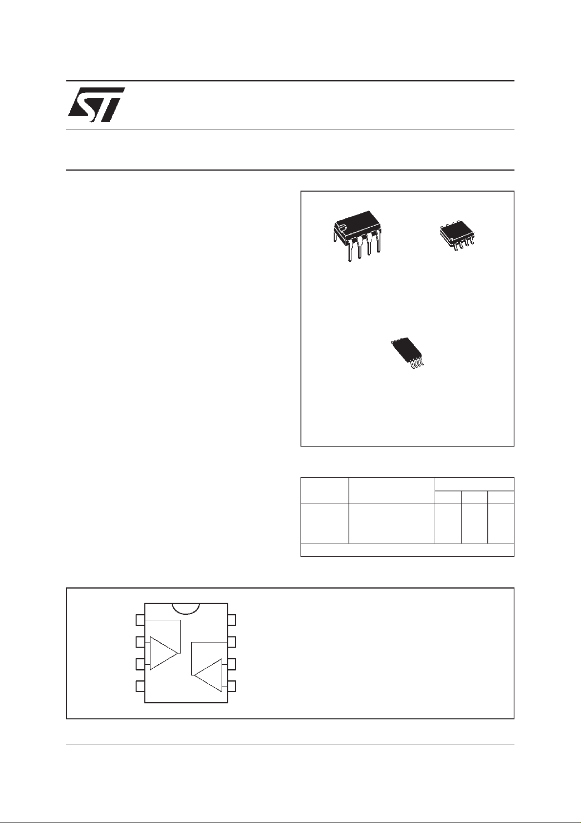
N
DIP8
(PlasticPackage)
(Thin Shrink Small Outline Package)
(PlasticMicropackage)
P
TSSOP8
LM393
D
SO8
DESC RIP TI ON
These devices consist of two independent low
powervoltagecomparatorsdesignedspecificallyto
operatefrom a single supply overa wide range of
voltages.Operationfromsplitpowersuppliesisalso
possible.
Thesecomparatorsalsohaveauniquecharacteristic in that the input common-modevoltagerange
includesgroundeventhoughoperatedfroma single
powersupplyvoltage.
PI N CONNECTIONS (top view)
1
2
-
+
3
45
8
7
6
-
+
ORDER CODES
Part
Number
LM193 –55, +125
LM293 –40, +105
LM393 0, +70
Example : LM393D
1 - Output1
2 - Invertinginput 1
3 - Non-inverting input 1
4-V
5 - Non-inverting input 2
6 - Invertinginput 2
7 - Output2
8-V
CC
CC
-
+
Temperature
Range
Package
o
C •••
o
C •••
o
C •••
NDP
June 1998
1/10
Page 2
LM193 - LM293 - LM 393
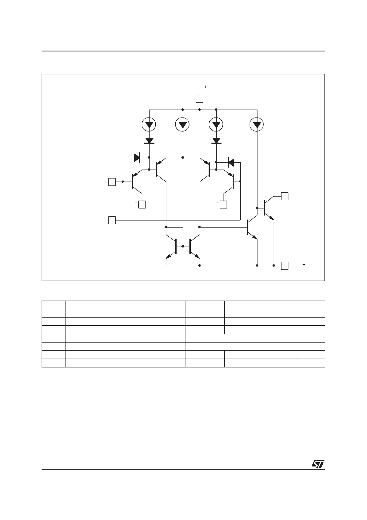
SCHE MATIC DIAGRAM (1/2 LM193)
V
CC
3.5µA100
µ
A 3.5µA 100µA
Non-inverting
Input
V
V
CC
V
CC
O
Inverting
Input
V
CC
ABSOLUTE MAXIMUM RATINGS
Symbol Parameter LM193 LM293 LM393 Unit
V
P
T
T
Notes : 1. Sho r t-cir cuit f r om t he output to V
Supply Voltage ±18 or 36 ±18 or 36 ±18 or 36 V
CC
Differential Input Voltage ±36 ±36 ±36 V
V
id
Input Voltage –0.3 to +36 –0.3 to +36 –0.3 to +36 V
V
i
Output Short-circuit to Ground – (note 1) Infinite
Power Dissipation 830 mW
tot
Operating Free-air TemperatureRange –55 to +125 –40 to +105 0 to +70
oper
Storage Temperature Range –65 to +150 –65 to +150 –65 to +150
stg
+
can cause excessive heati ng and eventual destruction. T he maxi mum out pu t
curr ent is approximately 20mA, independent of the magnitude of V
CC
+
.
CC
o
C
o
C
2/10
Page 3
ELECTRICAL CHARACTERISTICS
V
CC
+
= +5V, V
CC
–
= 0V, T
=25oC (unless otherwise specified)
amb
Symbol Parameter
Input Offset Voltage – (note 2)
V
io
Input Bias Current – (note 3)
I
ib
Input Offset Current
I
io
A
V
I
V
I
Notes : 2. At output switch p oint, VO≈ 1.4V, RS=0Ωwit h V
Large Signal Voltage Gain
vd
I
Supply Current (all comparators)
CC
Input Common Mode Voltage Range - (note 4)
icm
Differential Input Voltage - (note 6) V
V
id
Output Sink Current
sink
Low Level Output Voltage
OL
High Level Output Current
OH
Response Time
t
re
t
Large Signal Response Time
rel
(0V to V
3. T he dir ection of t he input curre nt is o ut of the IC d ue to the PN P input stage . Thi s curr ent i s essentially const ant ,
independent of the stat e of the out put, so no loading charge exists on the re ference or input l i nes.
4. T he input common-mode vo ltage of eit her inp ut signal vol t age should not be allow ed to go negative by more than
0.3V .
The upper end of the common- mode voltage r ange is V
damage.
5. T he r esponse ti m e specified is for a 100m V input step w ith 5mV overdri ve. For lar ger overdr i ve signals 300ns
can be obtai ne d.
6. P ositive excursions of i nput volt age may ex ceed the pow er supply level. As l ong as the other vol t age remains
wit hin the comm on- mode range t he com parator willprovi de a pr oper outpu t state. The low input volt age state must
not be less than –0.3V (or 0.3V below the negat i ve power supply, if used).
= +25oC
T
amb
. ≤ T
T
min
T
amb
. ≤ T
T
min
T
amb
. ≤ T
T
min
= 15V, RL= 15kΩ,Vo= 1 to 11V 50 200
V
CC
= 5V, no load
V
CC
= 30V, no load
V
CC
T
amb
. ≤ T
T
min
= -1V, VO= 1.5V) 6 16
(V
id
= -1V, I
(V
id
T
amb
. ≤ T
T
min
= 1V, VCC=VO= 30V)
(V
id
T
amb
. ≤ T
T
min
= 5.1kΩ to V
(R
L
=TTL,V
(V
i
amb
= +25oC
amb
= +25oC
amb
= +25oC
amb
=25oC
amb
=25oC
amb
+
1.5V) .
CC
≤ T
max.
≤ T
max.
≤ T
max.
≤ T
max.
= 4mA)
sink
≤ T
max
≤ T
max
+
) – (note 5) 1.3
CC
= +1.4 V, RL= 5.1kΩ to V
ref
CC
LM193 - LM293 - LM393
LM193 - LM293 - LM393
Min. Typ. Max.
15
25 250
550
0.4
1
0
0
250 400
0.1
+
) 300
+
fr om 5V to 30V and over the fu l l input commo n- mode range
CC
+
–1.5V , but e ither or both inputs can go to +30V without
CC
9
400
150
1
2.5
+
V
-1.5
CC
+
-2
V
CC
+
CC
700
1
Unit
mV
nA
nA
V/mV
mA
V
V
mA
mV
nA
µA
µs
ns
3/10
Page 4

LM193 - LM293 - LM 393
SUP PLY CURRENT ve rs us
SUPPLY VOLTAGE
1
0.8
0.6
0.4
0.2
SUPPLYCURRENT(mA)
0
10 20 30 40
SUPPLY VOLTAGE(V)
OUTPUT SATURATI ON VOLTAG E
ve rs us OUTP UT CURRENT
1
10
Out of saturation
0
10
T
=+125°C
amb
T
T
= +25°C
amb
10
-1
10
0
OUTPUT SINK CURRENT (mA)
SATURATIONVOLTAGE(V)
10
10
10
-1
-2
-3
10
-2
T
10
amb
T
amb
amb
1
=-55°C
T
=0°C
amb
T = +25°C
T
= +70°C
amb
= +125°C
R
=
L
= -55°C
10
INPUT CURRENT ver s us
SUPPLY VOLTAGE
80
V=0V
i
60
40
9
R=10Ω
i
T
=0°C
amb
T
amb
T
amb
= +25°C
= -55°C
20
T
= +125°C
INPUTCURRENT(nA)
amb
T
= +70°C
amb
0
10 20 30 40
SUPPLY VOLTAGE (V)
RESPONSE TIME FOR VARIOUS I NPUT
OVERDRI VE S - NEGATI VE TRANSITI O N
6
5
4
3
2
1
0
0
-50
-100
2
INPUTVOLTAGE(mV) OUTPUTVOLTAGE(V)
Input overdrive : 5mV
20mV
5V
e
I
100mV
T
= +25°C
amb
0 0.5 1 1.5 2
TIME (µs)
5.1kΩ
e
o
4/10
RESPO NSE TIM E FOR VARI OUS INPUT
OVERDRIVES - POS ITIVE TRANSITI ON
6
Input overdrive : 100mV
5
INPUTVOLTAGE(mV) OUTPUTVOLTAGE(V)
100
50
4
3
2
1
20mV
0
T
= +25°C
amb
0
0 0.5 1 1.5 2
TIME (µs)
5mV
5V
5.1 kΩ
e
I
e
o
Page 5

TYP ICAL APPLICATIONS
BASIC COMPARATOR
LM193 - LM293 - LM393
DRIVING CMOS
+V
(ref)
-V
(ref)
DRIV ING TTL
+V
(ref)
-V
(ref)
1/2
LM193
1/2
LM193
15k
5V
V
Ω
CC
10kΩ
=5V
&
&
5V
100kΩ
+V
(ref)
V
O
-V
(ref)
1/2
LM193
&
LOW FREQUENCY OP A MP
5V
15k Ω
1/2
~
e
1k
LM193
I
Ω
100k
e
0.5µF
o
Ω
A = 100
V
LO W FREQ UE N CY OP AMP
(e = 0Vfor e = 0V)
o
~
e
I
1k
Ω
1/2
LM193
100kΩ
I
A =100
V
15kΩ
0.5µF
5V
2N2222
TRANSDUCER AM PL I FI E R
5V
Magneticpick-up
e
o
10kΩ
10kΩ
1/2
LM193
20MΩ
3kΩ
e
o
5/10
Page 6

LM193 - LM293 - LM 393
LOW FREQUENCY OP AMP WITH OFFSET
ADJUST
5V
1MΩ
100kΩ
1kΩ
1MΩ
1/2
LM193
100k
15kΩ
0.5µF
R1
5V
2N2222
Ω
e
o
Offset Adjust
R2
R
s
e
~
I
R
I
TWO DECADES HIGH FREQUENCY VCO
Ω
100k
20k
1/2
LM193
Ω
+50V
Freque nc y co ntrol
voltage input
v
control
10k
0.1µF
Ω
20k
Ω
50k
V
=+30V
CC
+250mV
700 Hz f 100kHz
o
Ω
V
control
ZERO CROS SI N G DETECTOR
(SINGLE POWER SUPPLY)
100kΩ
5.1kΩ 5.1kΩ
e
I
1N4148
V
500pF
CC
1/2
LM193
Ω
3k
5.1k
0.01µF
Ω
V
CC
V
/2
CC
/2
100k
1/2
LM193
Ω
10kΩ
V
CC
100kΩ
1/2
LM193
Ω
3k
5V
5.1kΩ
20MΩ
Output 1
Output 2
LIMIT COMPARATOR
2R
S
R
S
~
2R
S
6/10
high
low
V
(ref)
e
I
V
(ref)
1/2
LM193
1/2
LM193
V
10kΩ
CRYSTAL CONTROLLED OSCILLATOR
=15V
Ω
V
CC
100kΩ
1/2
LM193
f = 100kHz
2k
Ω
V
CC
0
e
o
(12V)
CC
200kΩ
Lamp
2N 2222
193-17.EPS
0.1µF
200k
Page 7

SPLIT-SUPPLY APPLICATIONS
ZERO CROSSING DETECTOR
LM193 - LM293 - LM393
COMPARATOR WITH A NEGATIVE
REFERENCE
15V
5.1 k
Ω
1/2
e
~
I
LM193
15V
e
o
e
~
I
5V
1/2
LM193
15V
15V
5.1k
Ω
e
o
7/10
Page 8

LM193 - LM293 - LM 393
PACKAG E MECHANI CAL DATA
8 PINS -PLASTIC DIP
Dimensions
Min. Typ. Max. Min. Typ. Max.
Millimeters Inches
A 3.32 0.131
a1 0.51 0.020
B 1.15 1.65 0.045 0.065
b 0.356 0.55 0.014 0.022
b1 0.204 0.304 0.008 0.012
D 10.92 0.430
E 7.95 9.75 0.313 0.384
e 2.54 0.100
e3 7.62 0.300
e4 7.62 0.300
F 6.6 0260
i 5.08 0.200
L 3.18 3.81 0.125 0.150
Z 1.52 0.060
PM-DIP8.EPS
DIP8.TBL
8/10
Page 9

PACKAG E MECHANI CAL DATA
8 PINS -PLASTIC MICROPACKAGE (SO)
LM193 - LM293 - LM393
Dimensions
Min. Typ. Max. Min. Typ. Max.
Millimeters Inches
A 1.75 0.069
a1 0.1 0.25 0.004 0.010
a2 1.65 0.065
a3 0.65 0.85 0.026 0.033
b 0.35 0.48 0.014 0.019
b1 0.19 0.25 0.007 0.010
C 0.25 0.5 0.010 0.020
c1 45
o
(typ.)
D 4.8 5.0 0.189 0.197
E 5.8 6.2 0.228 0.244
e 1.27 0.050
e3 3.81 0.150
F 3.8 4.0 0.150 0.157
L 0.4 1.27 0.016 0.050
M 0.6 0.024
S8
Information furnished is believed to be accurate and reliable. However, STMicroelectronics assumes no responsibility for the
consequences of use of such information nor for any infringement of patents or other rights of third parties which may result
from its use. No license is granted by implication or otherwise under any patent or patent rights of STMicroelectronics.
Specifications mentioned in this publication are subject to change without notice. This publication supersedes and replaces all
information previously supplied. STMicroelectronics products are not authorized for use as critical components in life support
devices or systems without express written approval of STMicroelectronics.
The ST logo is a trademark of STMicroelectronics
o
(max.)
PM-SO8.EPS
SO8.TBL
1998 STMicroelectronics – Printed in Italy – All Rights Reserved
STMicroelectronics GROUP OF COMPANIES
Australia - Brazil - Canada - China - France - Germany - Italy - Japan - Korea - Malaysia - Malta- Mexico - Morocco
The Netherlands - Singapore - Spain - Sweden - Switzerland - Taiwan - Thailand - United Kingdo m- U.S.A.
ORDERCODE
9/10
Page 10

LM193 - LM293 - LM 393
PACKAGE MECHANICAL DATA
8 PINS - THIN SHRINK SMALL OUTLINE PACKAGE
Dim.
Min. Typ. Max. Min. Typ. Max.
Millimeters Inches
A 1.20 0.05
A1 0.05 0.15 0.01 0.006
A2 0.80 1.00 1.05 0.031 0.039 0.041
b 0.19 0.30 0.007 0.15
c 0.09 0.20 0.003 0.012
D 2.90 3.00 3.10 0.114 0.118 0.122
E 6.40 0.252
E1 4.30 4.40 4.50 0.169 0.173 0.177
e 0.65 0.025
k0
o
o
8
o
0
l 0.50 0.60 0.75 0.09 0.0236 0.030
o
8
10/10
 Loading...