

Page 1
LM2900/LM3900/LM3301 Quad Amplifiers
LM2900/LM3900/LM3301 Quad Amplifiers
February 1995
General Description
The LM2900 series consists of four independent, dual input,
internally compensated amplifiers which were designed
specifically to operate off of a single power supply voltage
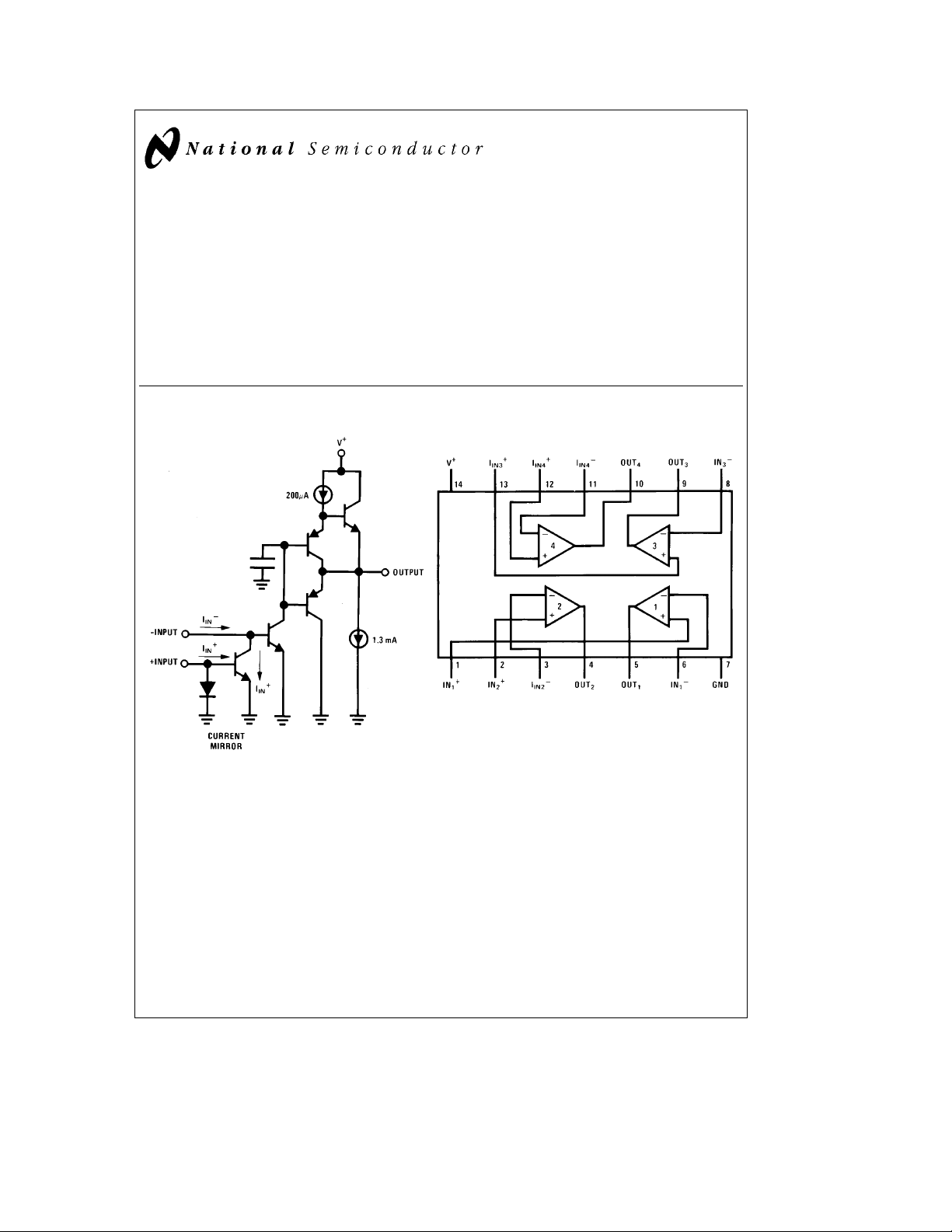
and to provide a large output voltage swing. These amplifiers make use of a current mirror to achieve the non-inverting input function. Application areas include: ac amplifiers,
RC active filters, low frequency triangle, squarewave and
pulse waveform generation circuits, tachometers and low
speed, high voltage digital logic gates.
Schematic and Connection Diagrams
Features
Y
Wide single supply voltage 4 VDCto 32 V
Range or dual supplies
Y
Supply current drain independent of supply voltage
Y
Low input biasing current 30 nA
Y
High open-loop gain 70 dB
Y
Wide bandwidth 2.5 MHz (unity gain)
Y
Large output voltage swing (V
Y
Internally frequency compensated for unity gain
Y
Output short-circuit protection
Dual-In-Line and S.O.
g
2VDCtog16 V
a
b
DC
DC
1) Vp-p
Top View
TL/H/7936– 2
Order Number LM2900N, LM3900M, LM3900N or LM3301N
TL/H/7936– 1
C
1995 National Semiconductor Corporation RRD-B30M115/Printed in U. S. A.
TL/H/7936
See NS Package Number M14A or N14A
Page 2
Absolute Maximum Ratings
If Military/Aerospace specified devices are required, please contact the National Semiconductor Sales Office/
Distributors for availability and specifications.
Supply Voltage 32 V
a
IN
e
25§C) (Note 1)
A
b
or I
IN
Power Dissipation (T
Molded DIP 1080 mW 1080 mW
S.O. Package 765 mW
Input Currents, I
Output Short-Circuit DurationÐOne Amplifier Continuous Continuous
e
T
25§C (See Application Hints)
A
Operating Temperature Range
LM2900
LM3900 0
Storage Temperature Range
Lead Temperature (Soldering, 10 sec.) 260
Soldering Information
Dual-In-Line Package
Soldering (10 sec.) 260
Small Outline Package
Vapor Phase (60 sec.) 215
Infrared (15 sec.) 220
See AN-450 ‘‘Surface Mounting Methods and Their Effect on Product Reliability’’ for other methods of soldering surface mount
devices.
ESD tolerance (Note 7) 2000V 2000V
Electrical Characteristics T
e
A
25§C, V
a
Parameter Conditions
Open Voltage Gain Over Temp.
Loop
Voltage Gain
Input Resistance
e
DV
10 V
O
Inverting Input
DC
Output Resistance 8 8 9 kX
Unity Gain Bandwidth Inverting Input 2.5 2.5 2.5 MHz
a
Input Bias Current Inverting Input, V
Inverting Input
e
5V
DC
Slew Rate Positive Output Swing 0.5 0.5 0.5
Negative Output Swing 20 20 20
Supply Current R
Output V
Voltage V
Swing
High R
OUT
V
Low I
OUT
V
High V
OUT
e %
On All Amplifiers 6.2 10 6.2 10 6.2 10 mA
L
e
2k, I
L
a
e
15.0 V
DCIIN
a
e
Absolute I
Maximum Ratings I
b
e
IN
a
e
b
e
IN
a
e
I
IN
b
e
IN
a
e
IN
e %
R
L
Output Source 6 18 6 10 5 18
Current
Capability
Sink (Note 2) 0.5 1.3 0.5 1.3 0.5 1.3 mA
b
I
SINK
e
V
OL
1V, I
e
5 mA555
IN
LM2900/LM3900 LM3301
DC
g
16 V
DC
20 mA
DC
b
40§Ctoa85§C
Ctoa70§C
§
b
65§Ctoa150§C
C 260§C
§
C 260§C
§
C 215§C
§
C 220§C
§
e
15 VDC, unless otherwise stated
LM2900 LM3900 LM3301
Min Typ Max Min Typ Max Min Typ Max
1.2 2.8 1.2 2.8 1.2 2.8
28 V
DC
g
14 V
DC
20 mA
DC
b
40§Ctoa85§C
b
65§Ctoa150§C
Units
V/mV
111MX
30 200 30 200 30 300
nA
V/ms
0,
13.5 13.5 13.5
0
10 mA,
0V
0.09 0.2 0.09 0.2 0.09 0.2
DC
0,
0 29.5 29.5 26.0
,
DC
DC
2
Page 3
a
Electrical Characteristics (Note 6), V
Parameter Conditions
Power Supply Rejection T
Mirror Gain
DMirror Gain
e
25§C, fe100 Hz 70 70 70 dB
A
@
20 mA (Note 3) 0.90 1.0 1.1 0.90 1.0 1.1 0.90 1 1.10
@
200 mA (Note 3) 0.90 1.0 1.1 0.90 1.0 1.1 0.90 1 1.10
@
20 mAto200mA (Note 3) 2 5 2 5 2 5 %
e
15 VDC, unless otherwise stated (Continued)
LM2900 LM3900 LM3301
Min Typ Max Min Typ Max Min Typ Max
Units
mA/mA
Mirror Current (Note 4) 10 500 10 500 10 500 mA
Negative Input Current T
e
25§C (Note 5) 1.0 1.0 1.0 mA
A
Input Bias Current Inverting Input 300 300 nA
Note 1: For operating at high temperatures, the device must be derated based on a 125§C maximum junction temperature and a thermal resistance of 92§C/W
which applies for the device soldered in a printed circuit board, operating in a still air ambient. Thermal resistance for the S.O. package is 131
Note 2: The output current sink capability can be increased for large signal conditions by overdriving the inverting input. This is shown in the section on Typical
Characteristics.
Note 3: This spec indicates the current gain of the current mirror which is used as the non-inverting input.
Note 4: Input V
therefore a typical design center for many of the application circuits.
Note 5: Clamp transistors are included on the IC to prevent the input voltages from swinging below ground more than approximately
currents which may result from large signal overdrive with capacitance input coupling need to be externally limited to values of approximately 1 mA. Negative input
currents in excess of 4 mA will cause the output voltage to drop to a low voltage. This maximum current applies to any one of the input terminals. If more than one
of the input terminals are simultaneously driven negative smaller maximum currents are allowed. Common-mode current biasing can be used to prevent negative
input voltages; see for example, the ‘‘Differentiator Circuit’’ in the applications section.
Note 6: These specs apply for
Note 7: Human body model, 1.5 kX in series with 100 pF.
match between the non-inverting and the inverting inputs occurs for a mirror current (non-inverting input current) of approximately 10 mA. This is
BE
40§CsT
s
a
85§C, unless otherwise stated.
A
b
C/W.
§
b
0.3 VDC. The negative input
Application Hints
When driving either input from a low-impedance source, a
limiting resistor should be placed in series with the input
lead to limit the peak input current. Currents as large as
20 mA will not damage the device, but the current mirror on
the non-inverting input will saturate and cause a loss of mirror gain at mA current levelsÐespecially at high operating
temperatures.
Precautions should be taken to insure that the power supply
for the integrated circuit never becomes reversed in polarity
or that the unit is not inadvertently installed backwards in a
test socket as an unlimited current surge through the resulting forward diode within the IC could cause fusing of the
internal conductors and result in a destroyed unit.
Output short circuits either to ground or to the positive power supply should be of short time duration. Units can be
destroyed, not as a result of the short circuit current causing
metal fusing, but rather due to the large increase in IC chip
dissipation which will cause eventual failure due to excessive junction temperatures. For example, when operating
from a well-regulated
with a 100 kX shunt-feedback resistor (from the output to
a
5VDCpower supply at T
e
25§C
A
the inverting input) a short directly to the power supply will
not cause catastrophic failure but the current magnitude will
be approximately 50 mA and the junction temperature will
be above T
current, 11 MX provides approximately 30 mA, an open cir-
max. Larger feedback resistors will reduce the
J
cuit provides 1.3 mA, and a direct connection from the output to the non-inverting input will result in catastrophic failure when the output is shorted to V
a
as this then places the
base-emitter junction of the input transistor directly across
the power supply. Short-circuits to ground will have magnitudes of approximately 30 mA and will not cause catastrophic failure at T
e
25§C.
A
Unintentional signal coupling from the output to the non-inverting input can cause oscillations. This is likely only in
breadboard hook-ups with long component leads and can
be prevented by a more careful lead dress or by locating the
non-inverting input biasing resistor close to the IC. A quick
check of this condition is to bypass the non-inverting input
to ground with a capacitor. High impedance biasing resistors used in the non-inverting input circuit make this input
lead highly susceptible to unintentional AC signal pickup.
Operation of this amplifier can be best understood by noticing that input currents are differenced at the inverting-input
terminal and this difference current then flows through the
external feedback resistor to produce the output voltage.
Common-mode current biasing is generally useful to allow
operating with signal levels near ground or even negative as
this maintains the inputs biased at
transistors (see note 5) catch-negative input voltages at approximately
b
0.3 VDCbut the magnitude of current flow has
a
VBE. Internal clamp
to be limited by the external input network. For operation at
high temperature, this limit should be approximately 100 mA.
This new ‘‘Norton’’ current-differencing amplifier can be
used in most of the applications of a standard IC op amp.
Performance as a DC amplifier using only a single supply is
not as precise as a standard IC op amp operating with split
supplies but is adequate in many less critical applications.
New functions are made possible with this amplifier which
are useful in single power supply systems. For example,
biasing can be designed separately from the AC gain as was
shown in the ‘‘inverting amplifier,’’ the ‘‘difference integrator’’ allows controlling the charging and the discharging of
the integrating capacitor with positive voltages, and the ‘‘frequency doubling tachometer’’ provides a simple circuit
which reduces the ripple voltage on a tachometer output DC
voltage.
DC
DC
3
Page 4
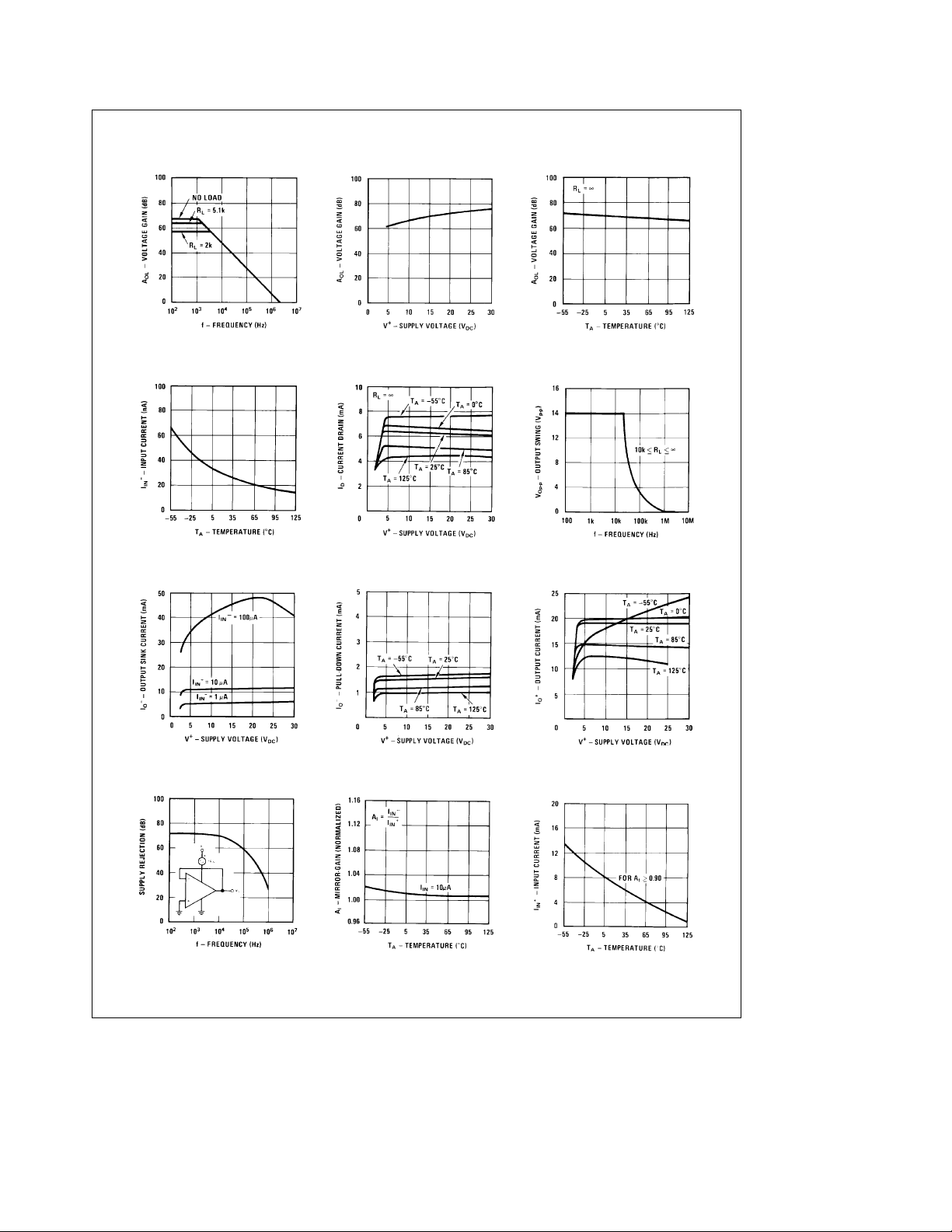
Typical Performance Characteristics
Open Loop Gain Voltage Gain Voltage Gain
Input Current Supply Current Response
Output Sink Current Output Class-A Bias Current Output Source Current
Supply Rejection Mirror Gain Maximum Mirror Current
Large Signal Frequency
TL/H/7936– 9
4
Page 5
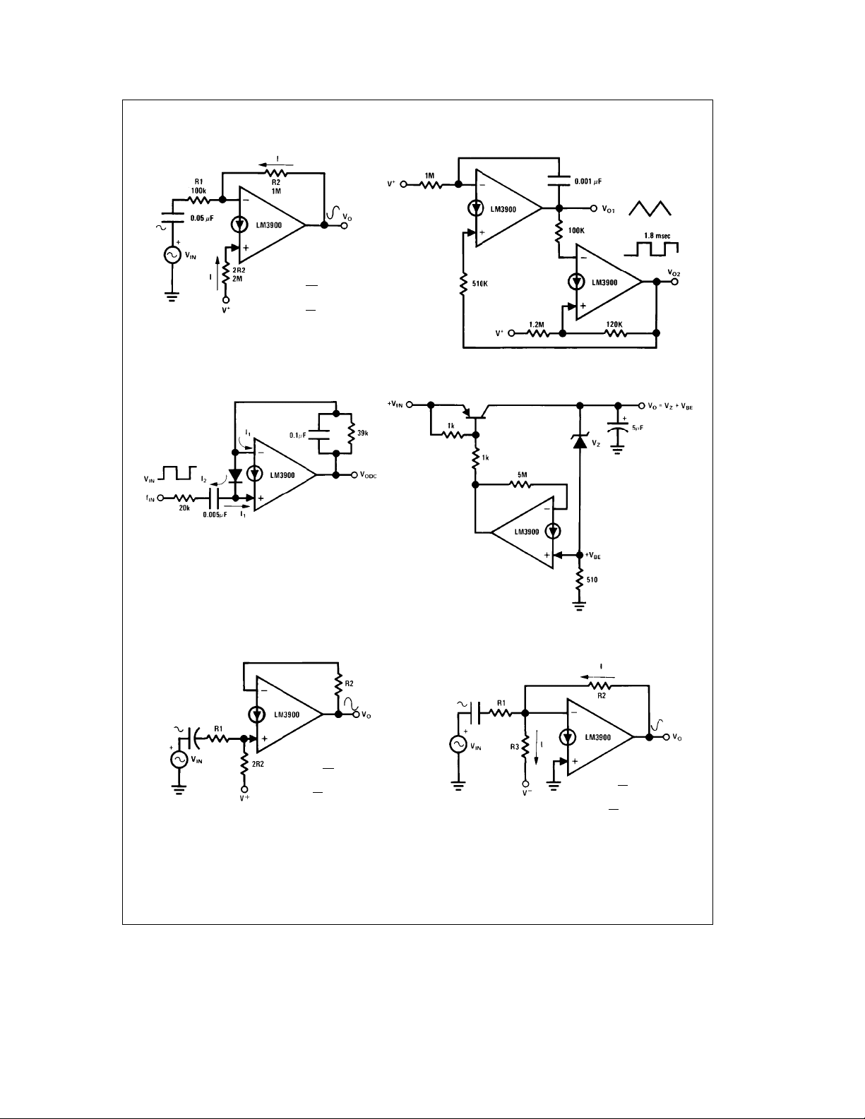
Typical Applications (V
Inverting Amplifier
V
ODC
j
A
V
e
b
a
e
a
V
2
R2
R1
15 VDC)
Triangle/Square Generator
TL/H/7936– 3
TL/H/7936– 4
Frequency-Doubling Tachometer
Non-Inverting Amplifier
V
e
V
ODC
R2
j
A
V
R1
TL/H/7936– 5
a
2
TL/H/7936– 7
Low V
b
V
IN
Voltage Regulator
OUT
Negative Supply Biasing
TL/H/7936– 6
R2
b
e
V
A
ODC
V
V
R3
R2
j
R1
TL/H/7936– 8
5
Page 6
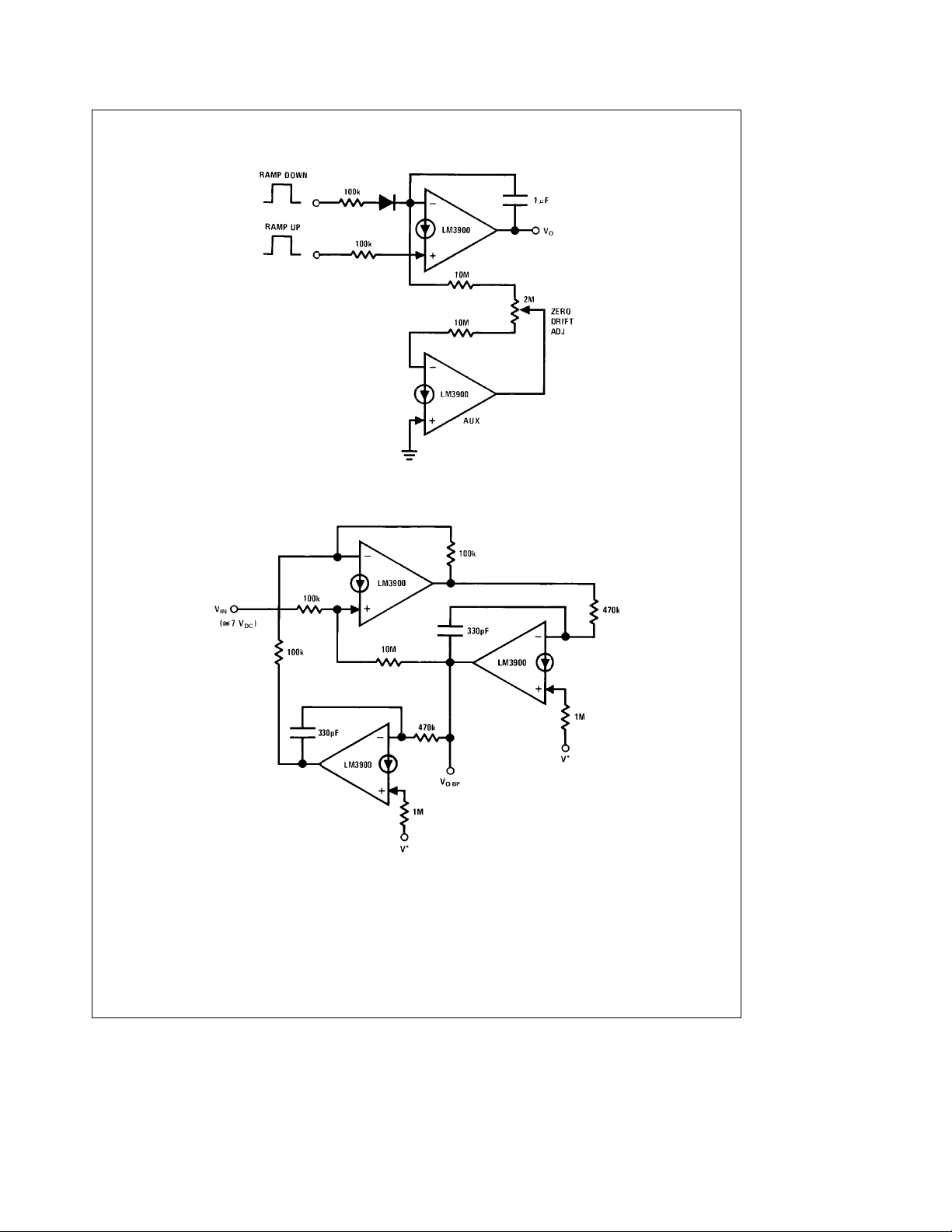
Typical Applications (V
a
e
15 VDC) (Continued)
Low-Drift Ramp and Hold Circuit
Bi-Quad Active Filter
(2nd Degree State-Variable Network)
TL/H/7936– 10
Qe50
e
f
1 kHz
O
TL/H/7936– 11
6
Page 7

Typical Applications (V
a
e
15 VDC) (Continued)
Voltage-Controlled Current Source
(Transconductance Amplifier)
TL/H/7936– 12
Q1 & Q2 absorb Hi V
Hi VIN,Lo(V
IN
b
VO) Self-Regulator
IN
Ground-Referencing a Differential Input Signal
TL/H/7936– 13
TL/H/7936– 14
7
Page 8

Typical Applications (V
Voltage Regulator
Voltage-Controlled Current Sink
(Transconductance Amplifier)
a
e
15 VDC) (Continued)
e
(V
V
O
Z
TL/H/7936– 15
Fixed Current Sources
a
VBE)
R1
e
I
I
2
1
R2
TL/H/7936– 16
Buffer Amplifier
TL/H/7936– 17
Tachometer
TL/H/7936– 19
8
V
e
V
Af
ODC
*Allows VOto go to zero.
IN
t
V
IN
BE
TL/H/7936– 18
Page 9

Typical Applications (V
Low-Voltage Comparator
No negative voltage limit if
properly biased.
a
e
15 VDC) (Continued)
Power Comparator
Comparator
Square-Wave Oscillator
TL/H/7936– 20
TL/H/7936– 22
TL/H/7936– 24
Frequency Differencing Tachometer
TL/H/7936– 21
Schmitt-Trigger
TL/H/7936– 23
Pulse Generator
TL/H/7936– 25
e
A(f
b
f2)
1
V
ODC
TL/H/7936– 26
9
Page 10

Typical Applications (V
a
e
15 VDC) (Continued)
Frequency Averaging Tachometer
e
A(f
a
f2)
1
TL/H/7936– 27
V
ODC
Squaring Amplifier (W/Hysteresis)
Differentiator (Common-Mode
Biasing Keeps Input at
a
VBE)
Bi-Stable Multivibrator
TL/H/7936– 29
TL/H/7936– 28
‘‘OR’’ Gate
feAaBaC
TL/H/7936– 31
‘‘AND’’ Gate
A
TL/H/7936– 30
feA#B#C
TL/H/7936– 32
1
e
V
2
Difference Integrator
TL/H/7936– 33
10
Page 11

Typical Applications (V
e
f
1 kHz
O
Staircase Generator
a
e
15 VDC) (Continued)
Low Pass Active Filter
TL/H/7936– 35
VBEBiasing
TL/H/7936– 34
R2
j
b
A
V
R1
Bandpass Active Filter
11
TL/H/7936– 36
e
f
1 kHz
o
e
Q
25
TL/H/7936– 37
Page 12

Typical Applications (V
a
e
15 VDC) (Continued)
Low-Frequency Mixer
Free-Running Staircase Generator/Pulse Counter
TL/H/7936– 38
TL/H/7936– 39
12
Page 13

Typical Applications (V
a
e
15 VDC) (Continued)
Supplying I
(to Allow Hi-Z Feedback Networks)
with Aux. Amp
IN
One-Shot Multivibrator
TL/H/7936– 40
PWj2c106C
*Speeds recovery.
TL/H/7936– 41
Non-Inverting DC Gain to (0,0)
TL/H/7936– 42
13
Page 14

Typical Applications (V
a
e
15 VDC) (Continued)
Channel Selection by DC Control (or Audio Mixer)
TL/H/7936– 43
14
Page 15

Typical Applications (V
a
e
15 VDC) (Continued)
Power Amplifier
One-Shot with DC Input Comparator
TL/H/7936– 44
High Pass Active Filter
15
a
Trips at V
VINmust fall 0.8 Vaprior to t
j
0.8 V
IN
TL/H/7936– 45
TL/H/7936– 46
2
Page 16

Typical Applications (V
a
e
15 VDC) (Continued)
Sample-Hold and Compare with New
a
V
IN
Sawtooth Generator
16
TL/H/7936– 47
TL/H/7936– 48
Page 17

Typical Applications (V
a
e
15 VDC) (Continued)
Boosting to 300 mA Loads
Phase-Locked Loop
TL/H/7936– 49
TL/H/7936– 50
17
Page 18

Split-Supply Applications (V
a
ea
15 VDC&V
Non-Inverting DC Gain
AC Amplifier
b
eb
15 VDC)
TL/H/7936– 51
TL/H/7936– 52
18
Page 19

Physical Dimensions inches (millimeters)
Small Outline Package (M)
Order Number LM3900M
NS Package Number M14A
19
Page 20

Physical Dimensions inches (millimeters) (Continued)
LM2900/LM3900/LM3301 Quad Amplifiers
Molded Dual-In-Line Package (N)
Order Number LM2900N, LM3900N or LM3301N
LIFE SUPPORT POLICY
NATIONAL’S PRODUCTS ARE NOT AUTHORIZED FOR USE AS CRITICAL COMPONENTS IN LIFE SUPPORT
DEVICES OR SYSTEMS WITHOUT THE EXPRESS WRITTEN APPROVAL OF THE PRESIDENT OF NATIONAL
SEMICONDUCTOR CORPORATION. As used herein:
1. Life support devices or systems are devices or 2. A critical component is any component of a life
systems which, (a) are intended for surgical implant support device or system whose failure to perform can
into the body, or (b) support or sustain life, and whose be reasonably expected to cause the failure of the life
failure to perform, when properly used in accordance support device or system, or to affect its safety or
with instructions for use provided in the labeling, can effectiveness.
be reasonably expected to result in a significant injury
to the user.
National Semiconductor National Semiconductor National Semiconductor National Semiconductor
Corporation Europe Hong Kong Ltd. Japan Ltd.
1111 West Bardin Road Fax: (
Arlington, TX 76017 Email: cnjwge@tevm2.nsc.com Ocean Centre, 5 Canton Rd. Fax: 81-043-299-2408
Tel: 1(800) 272-9959 Deutsch Tel: (
Fax: 1(800) 737-7018 English Tel: (
National does not assume any responsibility for use of any circuitry described, no circuit patent licenses are implied and National reserves the right at any time without notice to change said circuitry and specifications.
Fran3ais Tel: (
Italiano Tel: (
NS Package Number N14A
a
49) 0-180-530 85 86 13th Floor, Straight Block, Tel: 81-043-299-2309
a
49) 0-180-530 85 85 Tsimshatsui, Kowloon
a
49) 0-180-532 78 32 Hong Kong
a
49) 0-180-532 93 58 Tel: (852) 2737-1600
a
49) 0-180-534 16 80 Fax: (852) 2736-9960
 Loading...