

Page 1
LOW POWERDUAL VOLTAGE COMPARATORS
.WIDESINGLESUPPLYVOLTAGE RANGEOR
DUAL SUPPLIES +2V TO +36V OR ±1V TO
±18V
.VERYLOWSUPPLYCURRENT(0.4mA)INDE-
PENDENT OF SUPPLYVOLTAGE
(1 mW/comparator at +5V)
.LOW INPUT BIAS CURRENT : 25nA TYP
.LOW INPUT OFFSET CURRENT : ±5nA TYP
.INPUT COMMON-MODE VOLTAGE RANGE
INCLUDESGROUND
.LOW OUTPUT SATURATION VOLTAGE :
250mV TYP. (IO= 4mA)
.DIFFERENTIAL INPUT VOLTAGE RANGE
EQUAL TO THE SUPPLY VOLTAGE
.TTL, DTL, ECL, MOS, CMOS COMPATIBLE
OUTPUTS
DESCRIPTION
This device consistsof two independent low power
voltagecomparators designed specifically to operate from a single supply over a wide range of voltages. Operation from split power supplies is also
possible.
These comparators also have a unique
characteris-tic in the fact that the input common-mode voltage range includes ground even
though operated from a single power supply voltage.
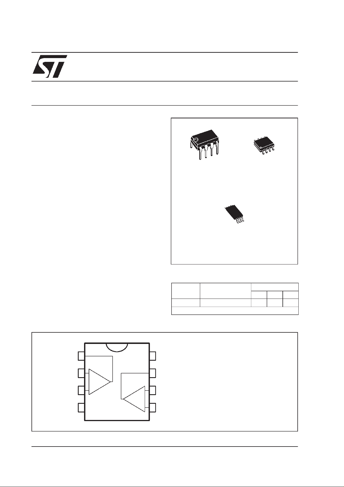
N
DIP8
(PlasticPackage)
(Thin ShrinkSmall Outline Package)
ORDER CODES
Part
Number
LM2903 -40, +125
Example : LM2903N
Temperature
Range
LM2903
(PlasticMicropackage)
P
TSSOP8
o
C
D
SO8
Package
NDP
•••
PIN CONNECTIONS (t op v ie w)
1
2
-
+
3
45
April 2000
8
1 - Output 1
7
-
+
6
2 - Inverting input 1
3 - Non-inverting input 1
-
4-V
CC
5 - Non-inverting input 2
6 - Inverting input 2
7 - Output 2
+
8-V
CC
1/10
Page 2
LM2903
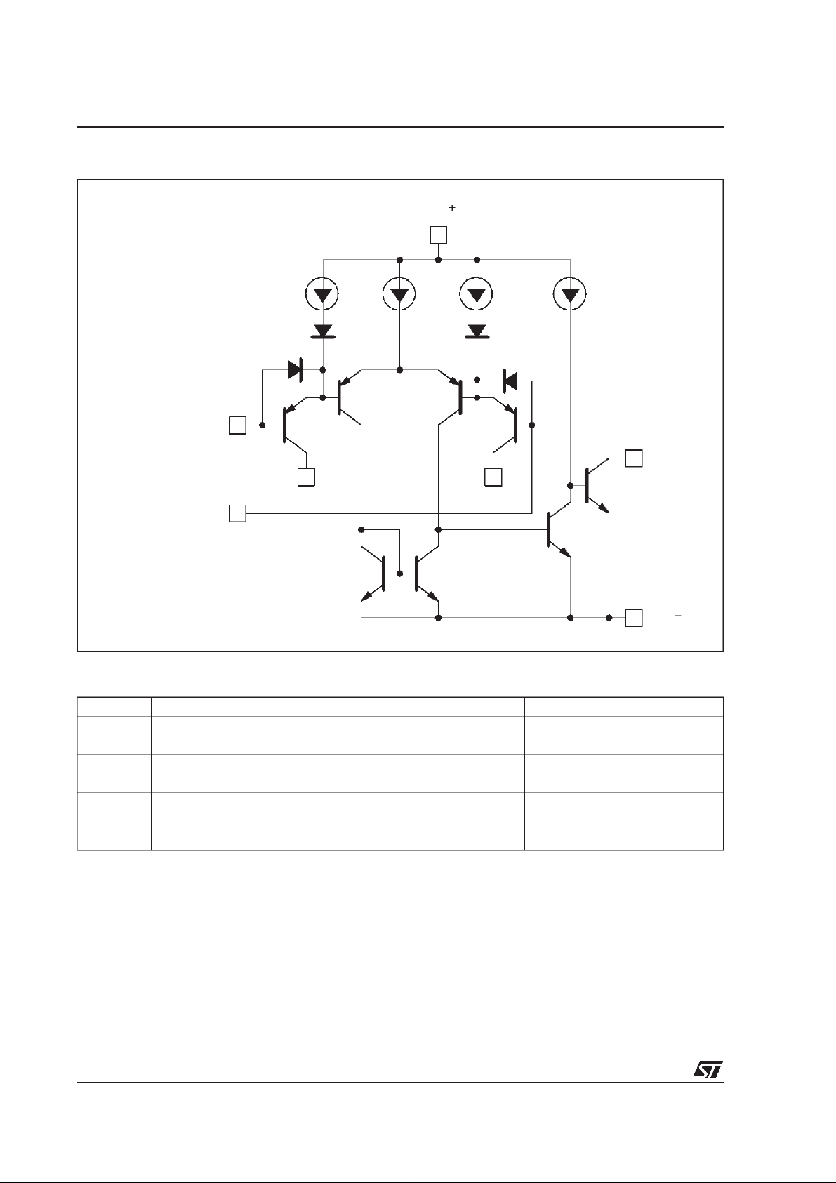
SCHEMATIC DIAGR AM (1/2 LM2903)
V
CC
3.5
µA
Non-inverting
Input
V
CC
Inverting
Input
ABSOLUTE MAXIMUM RATINGS
100
µA
V
3.5µA 100µA
CC
V
O
V
CC
Symbol Parameter Value Unit
V
CC
V
id
V
Supply Voltage
±18 or 36
Differential Input Voltage !36 V
Input Voltage -0.3 to +36 V
i
Output Short-circuit to Ground – (note 1) Infinite
P
tot
T
oper
T
stg
Notes : 1. Short-circuit f rom the output toV
Power Dissipation 830 mW
Operating Free-air TemperatureRange -40 to +125
Storage Temperature Range -65 to +150
+
can cause excessive heating and eventual destruction. The maximum output
current is approximately 20mA, i ndependent of the magnitude of V
CC
+
.
CC
2/10
V
o
C
o
C
Page 3

LM2903
ELECTRICAL CHARACTERISTICS
+
V
= +5V, V
CC
Symbol Parameter Min. Typ. Max. Unit
V
io
I
ib
I
io
A
vd
I
CC
V
icm
V
id
I
sink
V
OL
I
OH
t
re
t
rel
Notes : 2.
3. The directi on of thei nput current is out of the IC duet o the PNP input stage. This current isessenti ally constant,
4. The input common-mode voltage of either inputs ignal voltage should not beal lowed to go negative bym ore than
5. The response t i me specified is for a 100mV input step with 5mV overdrive.
6. Po sit ive excurs io ns of i nput vol tag e may exceed the power s upply l evel.
7. Maximum values are guaranteed by design.
–
CC
= 0V, T
=25oC (unless otherwise specified)
amb
Input Offset Voltage – (note 2)
T
amb
T
min
= +25oC
. ≤ T
amb
≤ T
max.
17
15
Input Bias Current – (note 3)
T
amb
T
min
= +25oC
. ≤ T
amb
≤ T
max.
25 250
400
Input Offset Current
T
= +25oC
amb
. ≤ T
T
min
amb
≤ T
max.
Large Signal Voltage Gain
V
= 15V, RL= 15kΩ,Vo= 1 to 11V
CC
25 200
550
150
V/mV
Supply Current (all comparators)
V
= 5V, no load
CC
V
= 30V, no load
CC
Input Common Mode Voltage Range (VCC= 30V) - (note 4)
T
amb
T
min
= +25oC
. ≤ T
amb
≤ T
max.
0
0
Differential Input Voltage - (note 6) V
0.4
1
1
2.5
+
V
-1.5
CC
+
V
-2
CC
+
CC
Output Sink Current
(V
= -1V, VO= 1.5V) 6 16
id
Low Level Output Voltage
(V
T
T
amb
min
= -1V, I
id
=25oC
. ≤ T
amb
sink
≤ T
= 4mA)
max.
250 400
700
High Level Output Current
(V
= 1V, VCC=VO= 30V)
id
T
=25oC
amb
. ≤ T
T
min
Small Signal Response Time
(R
L
Large Signal Response Time - (note 7)
TTL Input (V
Output Signal at 50% of final value
≤ T
amb
max.
= 5.1kΩ to V
ref
+
) - (note 5)
CC
= +1.4 V, RL= 5.1kΩ to V
+
)
CC
Output Signal at 95% of final value
At output switch point, VO#1.4V,RS=0Ωwith V
+
toV
1.5V).
CC
independent of t he state of the output, so no l oading charge exi sts on the reference or input li nes.
0.3V. T he upper end of the common-mode voltage range is V
without damage.
As long asthe other voltage remains w ithin thec ommon-mode range thecomparator wil lprovide a proper output
state. Thelow i nput voltagestat e mustnot beles s than–0.3V (or0. 3V belowt henegative power supply, if used).
+
from 5Vto30V andoverthe full inputcommon-mode range (0V
CC
+
–1.5V, but either or both inputs can go to +30V
CC
0.1
1
1.3
500
1
mV
nA
nA
mA
V
V
mA
mV
nA
µA
µs
ns
µs
3/10
Page 4

LM2903
SUPPLY CURRENT versus
SUPPLY VOLTAGE
1
0.8
0.6
0.4
0.2
SUPPLY CURRENT (mA)
0
10 20 30 40
SUP PLY VOLTAGE (V)
OUTPUT SATURATION VOLTAGE
versus OUTPUT CURRENT
1
10
Out ofsaturati on
0
10
T
=+125 C
amb
=+25 C
T
amb
10
-1
10
0
OUTPUT SINKCURRENT (mA)
SATURATION VOLTAGE (V)
10
10
10
-1
-2
-3
10
-2
T
T
10
amb
T
T
amb
T
amb
amb
1
=-55 C
=0 C
amb
=+25 C
T
=+70 C
amb
=+125 C
R
=
=-55 C
10
INPUT CURRENT versus
SUPPLY VOLTAGE
80
V=0V
i
60
40
R=10
i
T
amb
9
Ω
=0 C
T
=+25 C
amb
T
amb
=-55 C
20
=+125 C
T
INPUT CURRENT (nA)
amb
T
amb
0
10 20 30 40
SUPPLY VOLTAGE (V)
RESPONSE TIME FOR VARIOUS INPUT
OVERDRIVES - NEGATIVE TRANSITION
6
Input overdrive : 5mV
5
4
20mV
3
2
1
100mV
0
0
-50
-100
2
0 0.5 1 1.5 2
TIME(µs)
INPUT VOLTAGE (mV) OUTPUT VOLTAGE (V)
T
amb
e
I
=+25 C
=+70 C
5V
5.1kΩ
e
o
4/10
RESPONSE TIME FOR VARIOUS INPUT
OVERDRIVES - POSITIVE TRANSITION
6
Input overdrive : 100mV
5
INPUT VOLTAGE (mV) OUTPUT VOLTAGE (V)
100
50
4
3
2
1
20mV
0
T
= + 25 C
amb
0
0 0.5 1 1.5 2
TIME (µs)
5mV
5V
Ω
5.1k
e
I
e
o
Page 5

TYPIC AL APPLICATI O N S
BASIC COMPARATOR
LM2903
DRIVING CMOS
+V
(ref)
-V
(ref)
DRIVING TTL
+V
(ref)
-V
(ref)
1/2
LM2903
1/2
LM2903
VCC=5V
Ω
15k
5V
10k
Ω
&
&
V
5V
Ω
100k
+V
(ref)
O
-V
(ref)
LOWFREQUENCY OP AMP
~
e
1k
I
1/2
LM2903
Ω
1/2
LM2903
100k
A = 100
V
&
5V
Ω
15k
e
o
Ω
0.5µF
LOW FREQUENCY OP AMP
(e = 0V for e = 0V)
o
~
e
I
Ω
1k
I
1/2
LM2903
100k
A = 100
5V
15k
0.5µF
Ω
V
Ω
2N 2222
e
TR ANSD U CER AMPLIFIER
5V
Magnetic pick-up
Ω
o
10k
10k
Ω
1/2
LM2903
20M
Ω
3k
e
o
Ω
5/10
Page 6

LM2903
LOW FREQUENCY OP AMP WITH OFFSET
ADJUST
5V
Offse t Adjust
100k
Ω
5V
Ω
R2
R
s
~
e
I
1M
R
I
1k
Ω
1M
Ω
15k
1/2
LM2903
0.5µF
R1
100k
Ω
2N 2222
Ω
e
o
TW O D ECADES H IG H FREQUENCY VC O
Ω
100k
1/2
V
control
20k
+50V
LM2903
Ω
Frequencycon trol
voltage input
v
control
0.1µF
20k
Ω
50k
V
=+30V
CC
+250mV
700 Hz f 100kHz
Ω
o
ZERO CROSSING D ETE CT OR
(SI NGLE P OWER SUPP LY )
100k
5.1k
1N4148
LM2903
/2
Ω
100k
1/2
500pF
e
I
V
CC
1/2
LM2903
Ω
3k
5.1k
0.01µF
5.1k
V
CC
Ω
Ω
V
CC
/2
5V
Ω
Ω
10k
Ω
V
CC
100k
1/2
LM2903
20M
Ω
3k
Ω
Ω
Output 1
Output 2
5.1k
Ω
LIMIT COMPARATOR
2R
S
R
S
~
2R
S
6/10
high
low
V
(ref)
e
I
V
(ref)
1/2
LM2903
1/2
LM2903
10k
CRYSTAL CON TR O LLED OSC ILLATOR
V
(12V)
V
CC
Ω
0.1µF
200k
200k
Ω
Ω
Lamp
2N 2222
= 15V
CC
Ω
100k
1/2
LM2903
f = 100kHz
Ω
2k
V
CC
0
e
o
Page 7

LM2903
SPLIT-SUPPLY APPLICATIONS
ZERO CROSSING DETECTOR
15V
1/2
LM2903
~
e
I
15V
5.1k
COMPARAT OR WI TH A NEGATIV E REFERENCE
15V
Ω
e
o
~
e
I
1/2
LM2903
5.1k
Ω
e
o
5V
15V
7/10
Page 8

LM2903
PACKAGE MECHANICAL DATA
8 PINS -PLASTIC DIP
Dimensions
A 3.32 0.131
a1 0.51 0.020
B 1.15 1.65 0.045 0.065
b 0.356 0.55 0.014 0.022
b1 0.204 0.304 0.008 0.012
D 10.92 0.430
E 7.95 9.75 0.313 0.384
e 2.54 0.100
e3 7.62 0.300
e4 7.62 0.300
F 6.6 0260
i 5.08 0.200
L 3.18 3.81 0.125 0.150
Z 1.52 0.060
Min. Typ. Max. Min. Typ. Max.
Millimeters Inches
8/10
Page 9

PACKAGE MECHANICAL DATA
8 PINS -PLASTIC MICROPACKAGE (SO)
LM2903
Dimensions
Min. Typ. Max. Min. Typ. Max.
Millimeters Inches
A 1.75 0.069
a1 0.1 0.25 0.004 0.010
a2 1.65 0.065
a3 0.65 0.85 0.026 0.033
b 0.35 0.48 0.014 0.019
b1 0.19 0.25 0.007 0.010
C 0.25 0.5 0.010 0.020
c1 45
o
(typ.)
D 4.8 5.0 0.189 0.197
E 5.8 6.2 0.228 0.244
e 1.27 0.050
e3 3.81 0.150
F 3.8 4.0 0.150 0.157
L 0.4 1.27 0.016 0.050
M 0.6 0.024
S8
o
(max.)
9/10
Page 10

LM2903
PACKAGE MECHANICAL DATA
8 PINS -THIN SHRINK SMALL OUTLINE PACKAGE
c
E1
A2
A1
0,25 mm
.010 inch
GAGE PLANE
SEATING
5
PLANE
k
L
L1
C
EA
Dim.
D
b
Caaa
8
PIN 1 IDENTIFICATION
Millimeters Inches
Min. Typ. Max. Min. Typ. Max.
e
14
A 1.20 0.05
A1 0.05 0.15 0.01 0.006
A2 0.80 1.00 1.05 0.031 0.039 0.041
b 0.19 0.30 0.007 0.15
c 0.09 0.20 0.003 0.012
D 2.90 3.00 3.10 0.114 0.118 0.122
E 6.40 0.252
E1 4.30 4.40 4.50 0.169 0.173 0.177
e 0.65 0.025
k0
o
o
8
o
0
l 0.50 0.60 0.75 0.09 0.0236 0.030
o
8
Information furnished is believed to be accurate and reliable. However, STMicroelectronics assumes no responsibility for the
consequences of use of such information nor for any infringement of patents or other rights of third parties which may result
from its use. No license is granted by implication or otherwise under any patent or patent rights of STMicroelectronics. Specifications mentioned in this publication are subject to change without notice. This publication supersedes and replaces all information previously supplied. STMicroelectronics products are not authorized for use as critical components in life support
devices or systems without express written approval of STMicroelectronics.
The ST logo is a trademark of STMicroelectronics
2000 STMicroelectronics – Printed in Italy – All Rights Reserved
STMicroelectronics GROUP OF COMPANIES
Australia - Brazil - China - Finland - France - Germany - Hong Kong - India - Italy - Japan - Malaysia - Malta - Morocco
Singapore - Spain - Sweden - Switzerland - United Kingdom - U.S.A.
http://www.st.com
10/10
 Loading...