

Page 1
LOWPOWER QUAD VOLTAGE COMPARATORS
.WIDESINGLESUPPLYVOLTAGERANGEOR
DUAL SUPPLIES FOR ALL DEVICES: +2V TO
+36V OR ±1V TO ±18V
.VERYLOWSUPPLYCURRENT(1.1mA) IN-
DEPENDENT OF SUPPLY VOLTAGE
(1.4mW/comparatorat +5V)
.LOW INPUT BIAS CURRENT: 25nA TYP
.LOW INPUT OFFSET CURRENT : ±5nA TYP
.INPUT COMMON-MODE VOLTAGE RANGE
INCLUDES GROUND
.LOW OUTPUT SATURATION VOLTAGE :
250mV TYP. (IO= 4mA)
.DIFFERENTIAL INPUT VOLTAGE RANGE
EQUALTO THE SUPPLY VOLTAGE
.TTL, DTL, ECL, MOS, CMOS COMPATIBLE
OUTPUTS
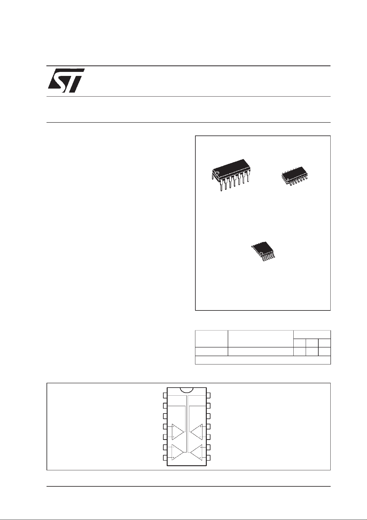
N
DIP14
(PlasticPackage)
LM2901
D
SO14
(PlasticMicropackage)
DESCRI PT ION
This device consists of four independent precision
voltage comparators. All these comparators were
designedspecificallytooperatefroma singlepower
supply over a wide range of voltages. Operation
fromsplit power supplies is also possible.
These comparators also have a unique
characteris-tic in that the input common-mode voltage range includes ground even though operated
froma singlepower supply voltage.
PIN CONNECTIONS (top view)
Output 2
Output 1
Inverting input 1
Non-inve rting input 1
Inverting input 2
Non-inve rting input 2
1
2
V
+
3
CC
4
5
6
7
TSSOP14
(Thin Shrink Small OutlinePackage)
ORDER CODES
Part
Number
LM2901 -40, +125
Example : LM2901D
14
Output 3
13
Output 4
12
V
CC
11
Non-inve rting input 4
10
Inverting input 4
9
Non-inve rting input 3
8
Inverting input 3
Temperature
Range
-
P
Package
o
C
NDP
•••
December1999
1/10
Page 2
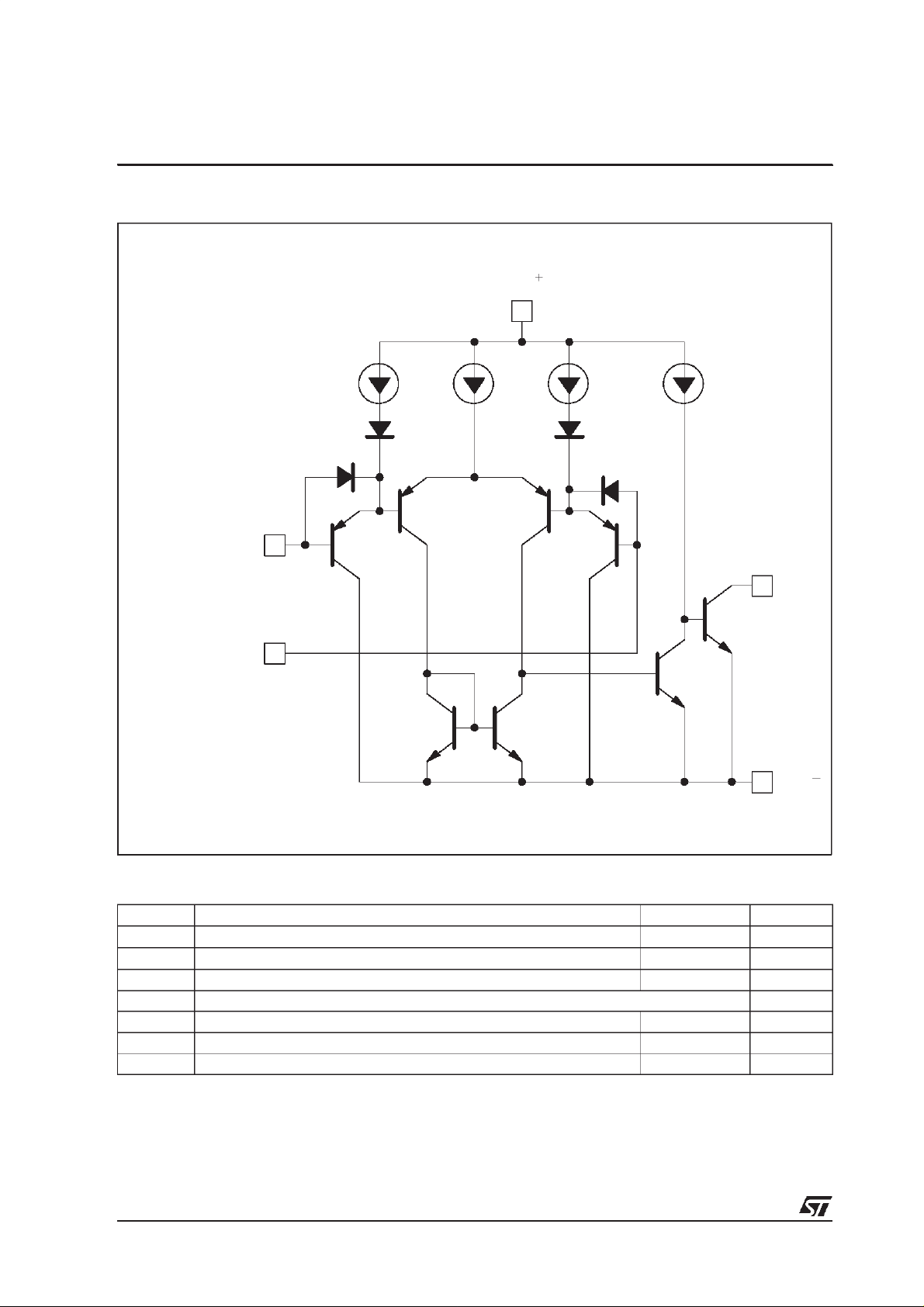
LM2901
SCHEMA TI C DIAGRAM ( 1/4 LM2901)
V
CC
Non-inverting
Input
Inverting
Input
µ
A 100µA3.5
3.5
µ
A 100µA
V
V
O
CC
ABSOLUTE MAXIMUM RATINGS
Symbol Parameter LM2901 Unit
V
V
V
P
T
oper
T
Notes : 1. Short-circuit f rom the output t o V
2/10
Supply Voltage
CC
Differential Input Voltage
id
Input Voltage -0.3 to +36 V
I
Output Short-circuit to Ground - note 1
Power Dissipation 570 mW
tot
Operating Free-air Temperature Range -40, +125
Storage Temperature Range -65, +150
stg
output current is approximately 20mA, i ndependent of the magnitude of V
+
can cause excessive heating and eventual destruction. The maximum
CC
CC
+
.
±18 to 36
±36
V
V
o
C
o
C
Page 3
LM2901
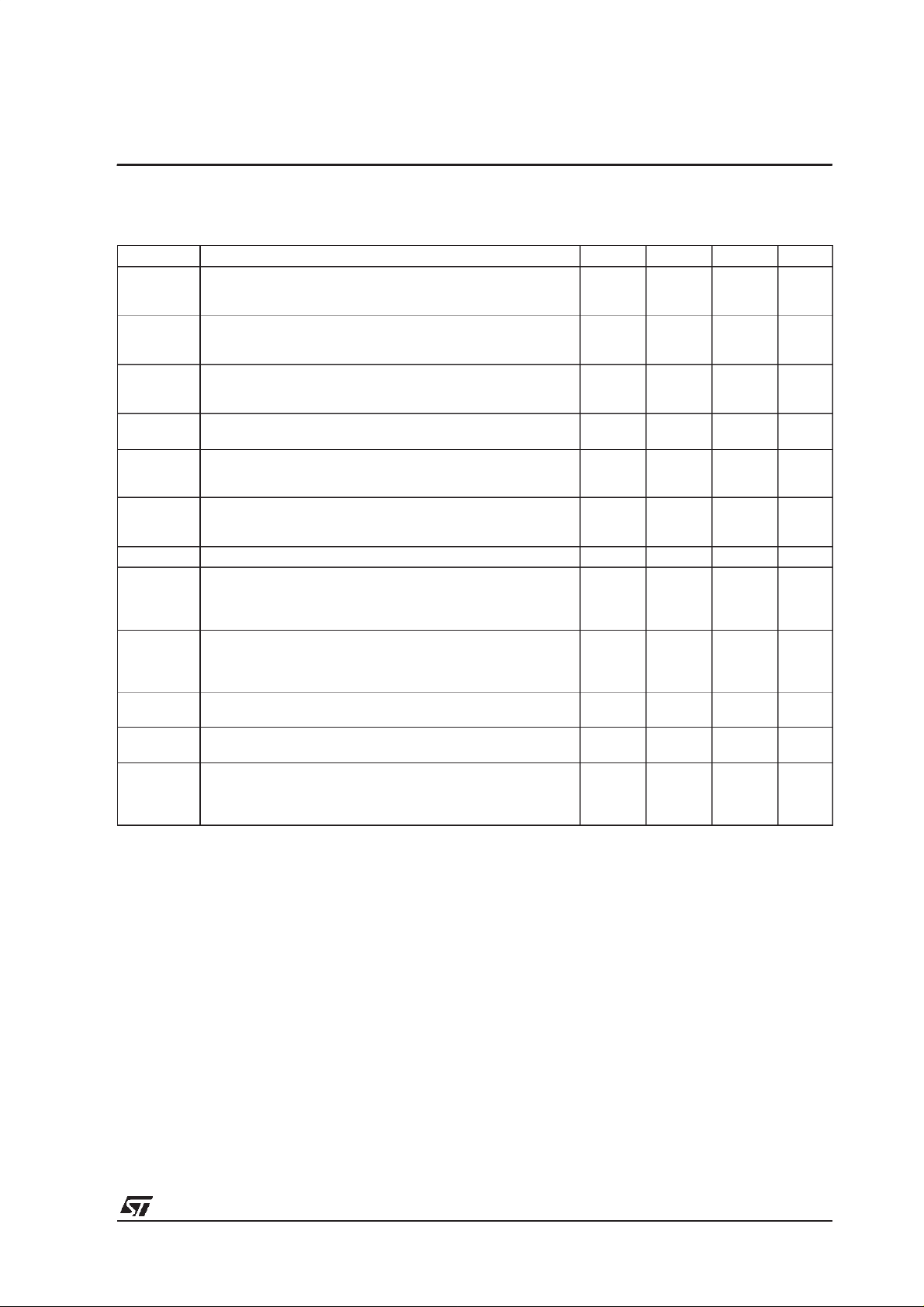
ELECTRICAL CHARACTERISTICS
+
V
= +5V, V
CC
Symbol Parameter Min. Typ. Max. Unit
V
io
I
io
I
ib
A
vd
I
CC
V
icm
V
id
V
OL
I
OH
I
sink
t
re
t
rel
Notes : 2.
At output sw itch point, VO≈ 1.4V , RS=0withV
range (0V to V
3. T he direction of the i nput current i s out of the IC due to the PNP i nput stage. This current is essentially
constant, independent of the state of the output, so no loading charge exists on the reference of i nput
lines.
4. T he input common-mode voltage of either input signal voltage should not be allowed to go negative by
more than 0.3V. The upper end of t he common-mode volt age range is V
can go to +30V without damage.
5. T he response time specifi ed is for a 100mV input step wi th 5mV overdrive.
6. P ositi ve excursions of i nput voltage may exceed the power supply level. As long as the other v oltage remains within the common-mode range, the comparator wi l l provide a proper output state. The low i nput
voltage state m ust not be less than –0.3V (or 0.3V bellow t he negative power supply, if used).
7. M aximum values are guaranteed by design.
-
= GND, T
CC
=25oC (unless otherwise specified)
amb
Input Offset Voltage - note 2
T
T
amb
min.
= +25oC
≤ T
amb
≤ T
max.
17
Input Offset Current
T
= +25oC
amb
T
≤ T
amb
≤ T
min.
Input Bias Current (I
T
= +25oC
amb
≤ T
T
min.
amb
≤ T
max.
+
I
max.
or I
–
) - note 3
I
550
25 250
Large Signal Voltage Gain
= 15V, RL=15kΩ,VO= 1 to 11V)
(V
CC
25 200
Supply Current (all comparators)
V
= +5V, no load
CC
V
= +30V, no load
CC
1.1
1.3
Input Common Mode Voltage Range (VCC= 30V) - note 4
T
T
amb
min
= +25oC
. ≤ T
amb
≤ T
max.
0
0
V
V
Differential Input Voltage - note 6 V
Low Level Output Voltage
(V
T
T
id
amb
min.
= -1V, I
= +25oC
≤ T
amb
sink
≤ T
= 4mA)
250 400
max.
High Level Output Current
(V
CC=VO
T
amb
T
min
= 30V, Vid= 1V)
= +25oC
. ≤ T
amb
≤ T
0.1
max.
Output Sink Current
(V
= -1V, VO= 1.5V) 6 16
id
Small Signal Response Time - (note 5)
= 5.1kΩ connected to V
(R
L
Large Signal Response Time - (note 7)
TTL Input (V
Output Signal at 50% of final value
= +1.4 V, RL= 5.1kΩ to V
ref
CC
+
)
+
)
CC
1.3
Output Signal at 95% of final value
+
from 5Vt o 30V, and over the full input common-mode
CC
+
–1.5V).
CC
+
–1.5V, but eit her or both inputs
CC
CC
15
150
400
2.5
CC
CC
700
500
2
+
1
1
-1.5
+
+
-2
mV
nA
nA
V/mV
mA
V
V
mV
nA
µA
mA
µs
ns
µs
3/10
Page 4

LM2901
SUPPLY CURRENT versus
SUPPLY VOLTAGE
0.8
0.6
0.4
0.2
SUPPLY CURRENT (mA)
1
0
10 20 30 40
SUPPLY VOLTAGE (V)
T
OUTPUT SATURATION VOLTAGE
versus OUTPUT CURRENT
1
10
Out of saturation
0
10
T
=+125 C
amb
T
=+25 C
T
amb
10
-1
10
0
10
OUTP UT SINKCURRENT (mA)
SATURATION VOLTAGE (V)
10
10
10
-2
-3
-1
10
-2
=-55 C
am b
T
amb
T = +2 5 C
amb
T
amb
T
amb
R
=-55 C
amb
1
=0 C
=+70 C
=+125 C
=
L
10
INPUT CURRENTversus
SUPPLY VOLTAGE
80
V=0V
i
60
40
R=10
i
T
amb
9
Ω
=0 C
T
=+25 C
amb
T
amb
=-55 C
20
=+125 C
T
INPUT CURRENT (nA)
amb
T
amb
0
10 20 30 40
SUPPLYVOLTAGE (V)
RESPON SE TIME FO R VARIOUS I NPUT
OVERDRIVES - NEGATIVE TRANSITION
6
Input ove rdrive : 5mV
5
4
20mV
3
2
100mV
1
0
0
-50
-100
2
INPUT VOLTAGE (mV) OUTPUT VOLTAGE (V)
0 0.5 1 1.5 2
TIME (µs)
T
e
amb
I
= +25 C
=+70 C
5V
5.1k
Ω
e
o
4/10
RESPONSE TIME FOR VARIOUS INPUT
OVERDRIVES - POSITIVE TRANSITION
6
Input o ve rdrive : 1 00 mV
5
INPUT VOLTAGE (mV) OUTPUT VOLTAGE (V)
4
3
2
1
0
100
50
0
=+25 C
T
amb
0 0. 5 1 1.5 2
20mV
TIME (
µ
5mV
s)
5V
Ω
5.1k
e
I
e
o
Page 5

TYPICA L APPLI CA TI O N S
LM2901
BASIC COMPARATOR
+V
(ref)
1/4
LM29 01
-V
(ref)
DRIVING TTL
+V
-V
(ref)
(ref)
1/4
LM2901
VCC=5V
Ω
15k
5V
10k
Ω
&
&
V
DRIVING CMOS
5V
Ω
100k
+V
(ref)
O
-V
(ref)
LOW F REQUENCY OP AMP
~
e
1k
LM2901
I
Ω
1/4
1/4
LM2901
Ω
100k
A = 100
V
5V
15k
0.5µF
&
Ω
e
o
LOW F REQUENCY OP AMP
(e = 0V for e = 0V)
o
~
e
I
Ω
1k
I
1/4
LM2901
100k
A = 100
5V
15k
0.5µF
Ω
V
Ω
2N 2222
e
TR ANSDUCER AMPLI F IER
5V
Magnetic pick-up
Ω
o
10k
10k
Ω
1/4
LM2901
20M
Ω
3k
e
o
Ω
5/10
Page 6

LM2901
TYPICAL APPLICATIONS (c onti nued)
TIME D ELAY GENERATOR
V
CC
=+15V
V
CC
0
tt
O
INPUT GATING SIGNAL
V
CC
V
3
V
V
C1
2
V
1
0
t
t
t
t
3
2
1
0
Ω
10k
Ω
10k
1/4
LM2901
A
V
(ref.)
15k
Ω
Ω
51k
V
C1
200k
V
3
V
Ω
Ω
10M
Ω
10k
1/4
LM2901
Ω
10M
Ω
10k
1/4
2
LM2901
3k
3k
Ω
V
CC
V
O3
t
t
0
3
Ω
V
CC
V
O2
t0t
2
0.001µF
Ω
3k
Ω
10M
Ω
51k
V
1
t
t
4
51k
Ω
10k
Ω
1/4
LM2901
V
V
CC
O1
t0t
1
LOW F REQUENCY OP AMP WITH OFFSET
ADJUST
5V
e
6/10
Offset Adjust
R2
R
s
~
I
1M
R
I
Ω
100k
Ω
Ω
1M
15k
1/4
LM2901
0.5µF
R1
100k
Ω
1k
5V
Ω
2N 2222
Ω
e
o
ZERO CROSSING DETECTOR
(single power supply)
Ω
100k
Ω
5.1k
e
I
5.1k
Ω
1N4148
10k
100k
LM2901
Ω
5V
Ω
1/4
20M
Ω
5.1k
Ω
Page 7

TYPICA L APPLI CA TI O N S (continued)
TWO- DEC AD E HIGH-F RE Q UE NC Y VCO
LM2901
Frequenc y control
voltage input
v
control
LIM IT COMPA RAT OR
2R
S
R
S
high
V
(ref)
Ω
100k
Ω
50k
V
CC
+250mV
700 Hz f 100kHz
V
CC
Ω
10k
1/4
LM2901
10k
0.1µF
20k
=+30V
(12V)
Ω
V
o
Lamp
Ω
control
20k
1/4
LM2901
Ω
+50V
500pF
V
1/4
LM2901
CC
Ω
3k
5.1k
0.01µF
100k
Ω
1/4
LM2901
V
/2
CC
V
/2
CC
V
CC
Ω
Ω
3k
Output 1
Output 2
CRYSTAL CONTROLLED OSCILLATOR
= 15V
V
CC
Ω
0.1µF
200k
100k
1/4
LM2901
Ω
2k
Ω
V
e
o
CC
0
e
~
I
1/4
LM2901
S
low
V
(ref)
2R
SPLIT-SU PPLY APPLICATIONS
ZERO CR OSSING DETECTOR
15V
1/4
LM2901
e
~
I
15V
2N 2222
5.1k
f= 100kHz
Ω
200k
COMPA RAT OR W ITH A NEGATIVE
REFERENCE
15V
Ω
Ω
1/4
e
o
e
~
I
LM2901
5.1k
e
o
5V
15V
7/10
Page 8

LM2901
PACKAGE MECHANICAL DATA
14 PINS - PLASTIC DIP
Dimensions
Min. Typ. Max. Min. Typ. Max.
Millimeters Inches
a1 0.51 0.020
B 1.39 1.65 0.055 0.065
b 0.5 0.020
b1 0.25 0.010
D 20 0.787
E 8.5 0.335
e 2.54 0.100
e3 15.24 0.600
F 7.1 0.280
i 5.1 0.201
L 3.3 0.130
Z 1.27 2.54 0.050 0.100
PM-DIP14.EPS
DIP14.TBL
8/10
Page 9

PACKAGE MECHANICAL DATA
14 PINS - P LASTI C MIC ROP ACKAGE (SO )
LM2901
Dim.
Min. Typ. Max. Min. Typ. Max.
Millimeters Inches
A 1.75 0.069
a1 0.1 0.2 0.004 0.008
a2 1.6 0.063
b 0.35 0.46 0.014 0.018
b1 0.19 0.25 0.007 0.010
C 0.5 0.020
c1 45
o
(typ.)
D 8.55 8.75 0.336 0.334
E 5.8 6.2 0.228 0.244
e 1.27 0.050
e3 7.62 0.300
F 3.8 4.0 0.150 0.157
G 4.6 5.3 0.181 0.208
L 0.5 1.27 0.020 0.050
M 0.68 0.027
S8
o
(max.)
PM-SO14.EP
SO14.TBL
9/10
Page 10

LM2901
PACKAGE MECHANICAL DATA
14 PINS - THIN SHRINK SMALL OUTLINE PACKAGE
c
E1
0,25 mm
.010 inch
GAGEPLANE
PLANE
SEATING
k
L
L1
C
E
e
78
1
Dim.
A
A2
A1
b
D
aaa
C
14
PIN 1 IDENTIFICATION
Millimeters Inches
Min. Typ. Max. Min. Typ. Max.
A 1.20 0.05
A1 0.05 0.15 0.01 0.006
A2 0.80 1.00 1.05 0.031 0.039 0.041
b 0.19 0.30 0.007 0.15
c 0.09 0.20 0.003 0.012
D 4.90 5.00 5.10 0.192 0.196 0.20
E 6.40 0.252
E1 4.30 4.40 4.50 0.169 0.173 0.177
e 0.65 0.025
k0
o
o
8
o
0
l 0.50 0.60 0.75 0.09 0.0236 0.030
o
8
nformation furnished is believed to be accurate and reliable. However, STMicroelectronics assumes no responsibility for the
consequences of use of such information nor for any infringement of patents or other rights of third parties which may result
from its use. No license is granted by implication or otherwise under any patent or patent rights of STMicroelectronics. Specifications mentioned in this publication are subject to change without notice. This publication supersedes and replaces all information previously supplied. STMicroelectronics products are not authorized for use as critical components in life support
devices or systems without express written approval of STMicroelectronics.
The ST logo is a trademark of STMicroelectronics
1999 STMicroelectronics – Printed in Italy – All Rights Reserved
STMicroelectronics GROUP OF COMPANIES
Australia - Brazil - China - Finland - France - Germany - Hong Kong - India - Italy - Japan - Malaysia - Malta - Morocco
Singapore - Spain - Sweden - Switzerland - United Kingdom - U.S.A.
http://www.st.com
10/10
ORDER CODE :
 Loading...