

Page 1
LM2878 Dual 5 Watt Power Audio Amplifier
LM2878 Dual 5 Watt Power Audio Amplifier
December 1994
General Description
The LM2878 is a high voltage stereo power amplifier designed to deliver 5W/channel continuous into 8X loads. The
amplifier is ideal for use with low regulation power supplies
due to the absolute maximum rating of 35V and its superior
power supply rejection. The LM2878 is designed to operate
with a low number of external components, and still provide
flexibility for use in stereo phonographs, tape recorders, and
AM-FM stereo receivers. The flexibility of the LM2878 allows it to be used as a power operational amplifier, power
comparator or servo amplifier. The LM2878 is internally
compensated for all gains greater than 10, and comes in an
11-lead single-in-line package (SIP). The package has been
redesigned, resulting in the slightly degraded thermal characteristics shown in the figure Device Dissipation vs Ambient Temperature.
Typical Applications
Features
Y
Wide operating range 6V –32V
Y
5W/channel output
Y
60 dB ripple rejection, output referred
Y
70 dB channel separation, output referred
Y
Low crossover distortion
Y
AC short circuit protected
Y
Internal thermal shutdown
Applications
Y
Stereo phonographs
Y
AM-FM radio receivers
Y
Power op amp, power comparator
Y
Servo amplifiers
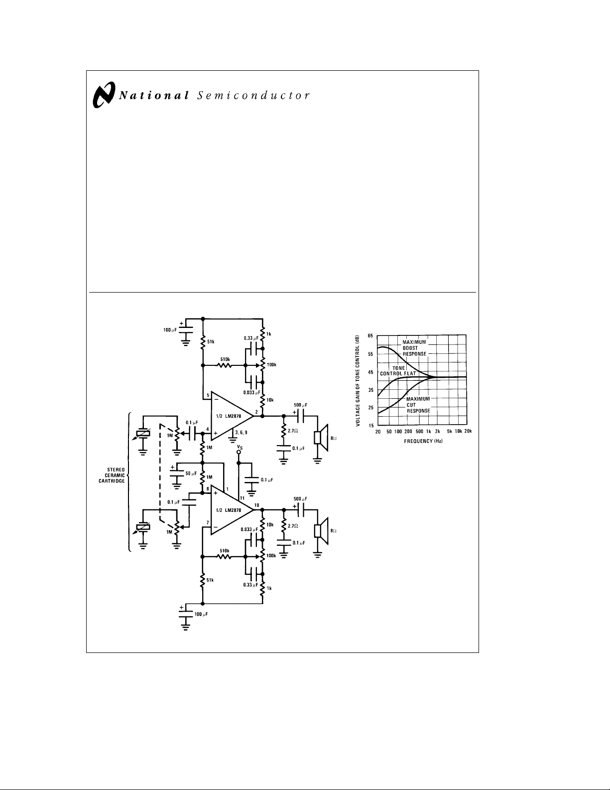
Frequency Response
of Bass Tone Control
TL/H/7934– 2
TL/H/7934– 1
FIGURE 1. Stereo Phonograph Amplifier with Bass Tone Control
C
1995 National Semiconductor Corporation RRD-B30M115/Printed in U. S. A.
TL/H/7934
Page 2
Absolute Maximum Ratings
If Military/Aerospace specified devices are required,
please contact the National Semiconductor Sales
Office/Distributors for availability and specifications.
Supply Voltage 35V
Input Voltage (Note 1)
Operating Temperature (Note 2) 0§Ctoa70§C
Electrical Characteristics V
g
0.7V
e
22V, T
S
TAB
Storage Temperature
Junction Temperature
Lead Temperature (Soldering, 10 sec.)
Thermal Resistance
i
JC
i
JA
e
25§C, R
e
L
8X,A
e
50 (34 dB) unless otherwise specified.
V
b
65§Ctoa150§C
a
a
10§C/W
55§C/W
150§C
260§C
Parameter Conditions Min Typ Max Units
Total Supply Current P
e
0W 10 50 mA
O
Operating Supply Voltage 6 32 V
Output Power/Channel fe1 kHz, THDe10%, T
e
f
1 kHz, THDe10%, V
Distortion fe1 kHz, R
e
P
O
e
P
O
e
P
O
Output Swing R
Channel Separation C
PSRR Power Supply C
Rejection Ratio f
e
L
BYPASS
e
f
1 kHz, Output Referred
e
V
O
BYPASS
e
120 Hz, Output Referred
V
ripple
e
8X
L
50 mW
0.5W 0.15 %
2W 0.14 %
8X V
e
50 mF, C
4 Vrms
e
50 mF, C
e
1 Vrms
PSRR Negative Supply Measured at DC, Input Referred
Common-Mode Range Split Suppliesg15V, Pin 1
Tied to Pin 11
e
25§C 5 5.5 W
TAB
e
12V 1.3 W
S
0.20 %
b
6V Vp-p
S
e
0.1 mF
IN
e
0.1 mF
IN
b
50
b
50
b
70 dB
b
60 dB
b
60 dB
g
13.5 V
Input Offset Voltage 10 mV
Noise Equivalent Input Noise
e
0, C
e20b
e
0.1 mF 2.5 mV
IN
20 kHz
R
BW
S
CCIR#ARM 3.0 mV
Open Loop Gain R
Output Noise Wideband
e
R
S
S
e
0, C
0.1 mF, A
IN
e
51X,fe1 kHz, R
e
200
V
e
8X 70 dB
L
0.8 mV
Input Bias Current 100 nA
Input Impedance Open Loop 4 MX
DC Output Voltage V
e
22V 10 11 12 V
S
Slew Rate 2V/mS
Power Bandwidth 3 dB Bandwidth at 2.5W 65 kHz
Current Limit 1.5 A
Note 1:g0.7V applies to audio applications; for extended range, see Application Hints.
Note 2: For operation at ambient temperature greater than 25
resistance which depends upon device mounting techniques.
C, the LM2878 must be derated based on a maximum 150§C junction temperature using a thermal
§
2
Page 3
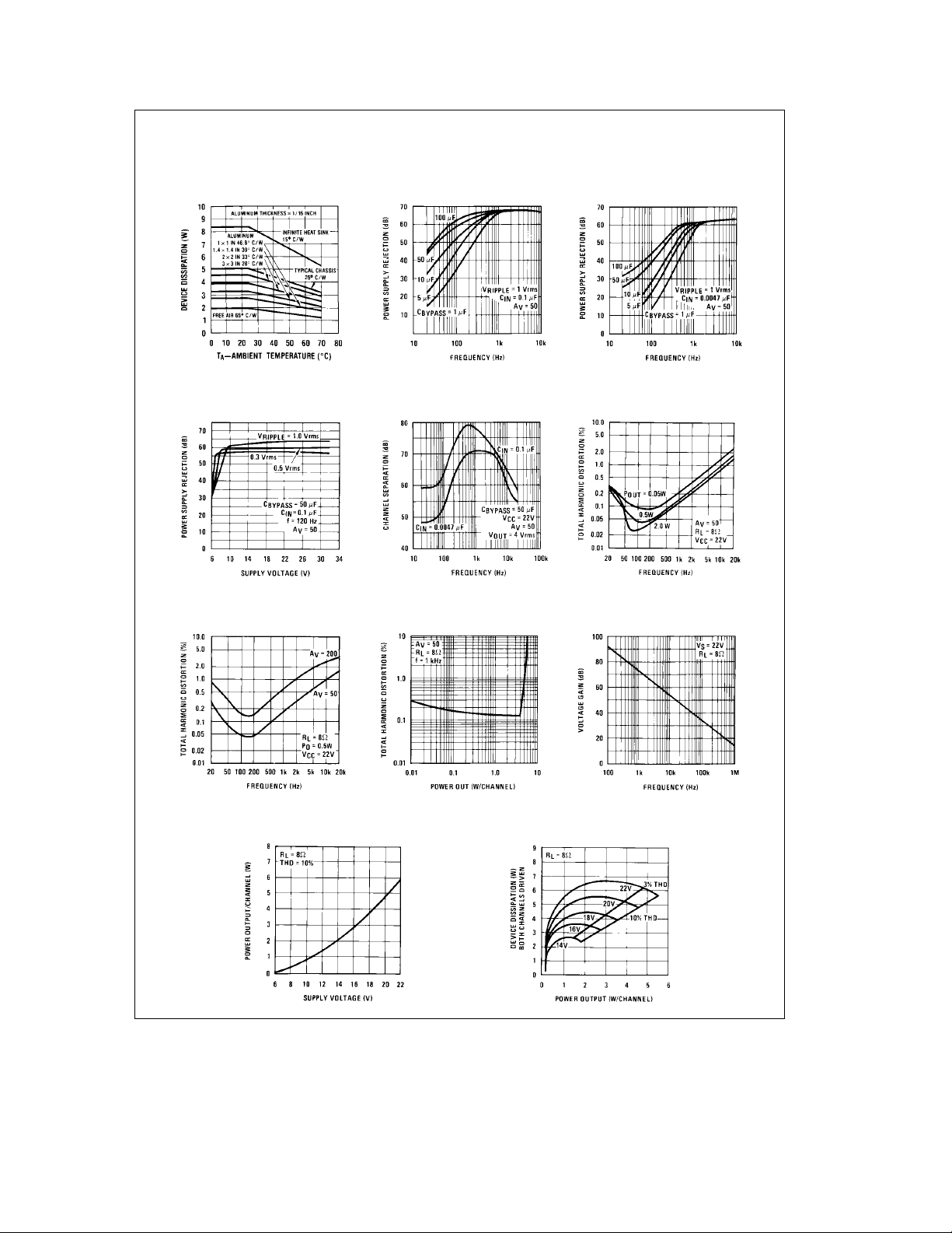
Typical Performance Characteristics
Device Dissipation vs
Ambient Temperature
Power Supply Rejection
Ratio (Referred to the
Output) vs Supply Voltage
Total Harmonic Distortion
vs Frequency
Power Supply Rejection
Ratio (Referred to the
Output) vs Frequency
Channel Separation
(Referred to the Output) vs
Frequency
Total Harmonic Distortion
vs Power Out
Power Supply Rejection
Ratio (Referred to the
Output) vs Frequency
Total Harmonic Distortion
vs Frequency
Open Loop Gain vs
Frequency
Power Output/Channel vs
Supply Voltage
Power Dissipation vs
Power Out
TL/H/7934– 3
3
Page 4

Equivalent Schematic Diagram
TL/H/7934– 4
4
Page 5

Connection Diagram
Single-In-Line Package
Application Hints
The LM2878 is an improved LM378 in typical audio applications. In the LM2878, the internal voltage regulator for the
input stage is generated from the voltage on pin 1. Normally,
the input common-mode range is within
voltage. Nevertheless the common-mode range can be increased by externally forcing the voltage on pin 1. One way
to do this is to short pin 1 to the positive supply, pin 11.
The only special care required with the LM2878 is to limit
the maximum input differential voltage to
ential voltage is exceeded, the input characteristics may
change.
Figure 2
shows a power op amp application with A
The 100k and 10k resistors set a noise gain of 10 and are
dictated by amplifier stability. The 10k resistor is bootstrapped by the feedback so the input resistance is dominated by the 1 MX resistor.
g
0.7V of this pin 1
g
7V. If this differ-
V
e
1.
*Pin 6 must be connected to GND.
Top View
Order Number LM2878P
See NS Package Number P11A
TL/H/7934– 5
FIGURE 2. Operational Power Amplifier, A
TL/H/7934– 6
e
1
V
5
Page 6

External Components
1. R2, R5, R7, R10 Sets voltage gain A
one channel and A
the other channel.
(Figure 3)
e1a
V
e1a
V
R2/R5 for
R10/R7 for
2. R4, R8 Resistors set input impedance and supply bias current for the positive input.
3. R
O
Works with COto stabilize output stage.
4. C1 Improves power supply rejection (see
Typical Performance Characteristics).
5. C11 Stabilizes amplifier, may need to be larger depending on power supply filtering.
Typical Applications (Continued)
6. C4, C8 Input coupling capacitor. Pins 4 and 8
are at a DC potential of V
quency pole set by:
1
e
f
L
2qR4C4
/2. Low fre-
S
7. C5, C7 Feedback capacitors. Ensure unity gain
at DC. Also low frequency pole at:
1
e
f
L
2qR5C5
8. C
O
Works with ROto stabilize output stage.
9. C2, C10 Output coupling capacitor. Low frequency pole given by:
1
e
f
L
RqRLC2
FIGURE 3. Stereo Amplifier with A
e
V
TL/H/7934– 7
200
FIGURE 4. LM2878 Servo Amplifier in
TL/H/7934– 8
Bridge Configuration
6
Page 7

Typical Applications (Continued)
k
(/4V
l
(/4V
*/4V
a
V
IN
a
to */4V
a
Truth Table
High Low
Off On
a
Off Off
On Off
FIGURE 5. Window Comparator Driving High, Low Lamps
TL/H/7934– 9
7
Page 8

Physical Dimensions inches (millimeters)
LM2878 Dual 5 Watt Power Audio Amplifier
Single-In-Line Package (P)
Order Number LM2878P
NS Package Number P11A
LIFE SUPPORT POLICY
NATIONAL’S PRODUCTS ARE NOT AUTHORIZED FOR USE AS CRITICAL COMPONENTS IN LIFE SUPPORT
DEVICES OR SYSTEMS WITHOUT THE EXPRESS WRITTEN APPROVAL OF THE PRESIDENT OF NATIONAL
SEMICONDUCTOR CORPORATION. As used herein:
1. Life support devices or systems are devices or 2. A critical component is any component of a life
systems which, (a) are intended for surgical implant support device or system whose failure to perform can
into the body, or (b) support or sustain life, and whose be reasonably expected to cause the failure of the life
failure to perform, when properly used in accordance support device or system, or to affect its safety or
with instructions for use provided in the labeling, can effectiveness.
be reasonably expected to result in a significant injury
to the user.
National Semiconductor National Semiconductor National Semiconductor National Semiconductor
Corporation Europe Hong Kong Ltd. Japan Ltd.
1111 West Bardin Road Fax: (
Arlington, TX 76017 Email: cnjwge@tevm2.nsc.com Ocean Centre, 5 Canton Rd. Fax: 81-043-299-2408
Tel: 1(800) 272-9959 Deutsch Tel: (
Fax: 1(800) 737-7018 English Tel: (
National does not assume any responsibility for use of any circuitry described, no circuit patent licenses are implied and National reserves the right at any time without notice to change said circuitry and specifications.
Fran3ais Tel: (
Italiano Tel: (
a
49) 0-180-530 85 86 13th Floor, Straight Block, Tel: 81-043-299-2309
a
49) 0-180-530 85 85 Tsimshatsui, Kowloon
a
49) 0-180-532 78 32 Hong Kong
a
49) 0-180-532 93 58 Tel: (852) 2737-1600
a
49) 0-180-534 16 80 Fax: (852) 2736-9960
 Loading...