

Page 1
LM2877 Dual 4W Audio Power Amplifier
LM2877 Dual 4W Audio Power Amplifier
February 1995
General Description
The LM2877 is a monolithic dual power amplifier designed
to deliver 4W/channel continuous into 8X loads. The
LM2877 is designed to operate with a low number of external components, and still provide flexibility for use in stereo
phonographs, tape recorders and AM-FM stereo receivers,
etc. Each power amplifier is biased from a common internal
regulator to provide high power supply rejection and output
Q point centering. The LM2877 is internally compensated
for all gains greater than 10, and comes in an 11-lead single-in-line package.
Features
Y
4W/channel
Y
b
68 dB ripple rejection, output referred
Y
b
70 dB channel separation, output referred
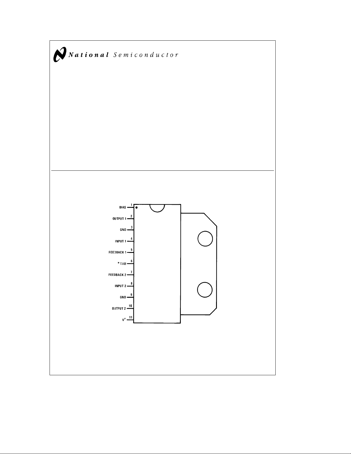
Connection Diagram
(Single-In-Line Package)
Y
Wide supply range, 6-24V
Y
Very low cross-over distortion
Y
Low audio band noise
Y
AC short circuit protected
Y
Internal thermal shutdown
Applications
Y
Multi-channel audio systems
Y
Stereo phonographs
Y
Tape recorders and players
Y
AM-FM radio receivers
Y
Servo amplifiers
Y
Intercom systems
Y
Automotive products
Top View
TL/H/7933– 1
Order Number LM2877P
See NS Package Number P11A
*Pin 6 must be connected to GND.
C
1995 National Semiconductor Corporation RRD-B30M75/Printed in U. S. A.
TL/H/7933
Page 2
Absolute Maximum Ratings
If Military/Aerospace specified devices are required,
please contact the National Semiconductor Sales
Office/Distributors for availability and specifications.
Supply Voltage 26V
Ctoa70§C
§
e
20V, T
S
g
0.7V
TAB
Input Voltage
Operating Temperature 0
Electrical Characteristics V
Storage Temperature
Junction Temperature 150§C
Lead Temperature (Soldering, 10 sec.) 260§C
Thermal Resistance
i
JC
i
JA
e
25§C, R
e
L
8X,A
e
50 (34 dB) unless otherwise specified.
V
Parameter Conditions Min Typ Max Units
Total Supply Current P
e
0W 25 50 mA
O
Operating Supply Voltage 6 24 V
Output Power/Channel fe1 kHz, THDe10%, T
e
V
20V 4.0 4.5 W
S
e
V
18V 3.6 W
S
e
V
S
e
V
S
Distortion, THD fe1 kHz, V
e
P
O
e
P
O
e
P
O
e
f
1 kHz, V
e
P
O
e
P
O
e
P
O
Output Swing R
Channel Separation C
PSRR Power Supply C
e
L
e
F
Output Referred
e
V
S
e
V
S
e
F
e
12V, R
12V, R
50 mW/Channel 0.1 %
4X 1.5 1.9 W
L
e
8X 1.0 W
L
e
20V
S
1W/Channel 0.07 1 %
2W/Channel 0.07 %
e
12V, R
S
50 mW/Channel 0.25 %
500 mW/Channel 0.20 %
1W/Channel 0.15 1 %
8X V
O
O
IN
e
e
0.5 Vrms
IN
e
4 Vrms
e
0.1 mF, fe1 kHz,
0.1 mF, fe120 Hz
50 mF, C
20V, V
7V, V
50 mF, C
e
25§C
TAB
e
4X
L
S
b
50
b
b
Rejection Ratio Output Referred
e
V
20V, V
S
e
V
7V, V
S
RIPPLE
RIPPLE
e
e
0.5 Vrms
1 Vrms
b
50
b
b
Noise Equivalent Input Noise
e
0, C
IN
e
0, C
IN
e
0, fe1 kHz, R
e
0.1 mF, BWe20 Hz–20 kHz 2.5 mV
e
0.1 mF, A
e
200 0.80 mV
V
e
8X 70 dB
L
Open Loop Gain R
R
S
Output Noise Wideband
R
S
S
Input Offset Voltage 15 mV
Input Bias Current 50 nA
Input Impedance Open Loop 4 MX
DC Output Level V
e
20V 9 10 11 V
S
Slew Rate 2.0 V/ms
Power Bandwidth 65 kHz
Current Limit 1.0 A
Note 1: For operation at ambient temperature greater than 25§C, the LM2877 must be derated based on a maximum 150§C junction temperature using a thermal
resistance which depends upon device mounting techniques.
b
65§Ctoa150§C
10§C/W
55§C/W
b
4V
p-p
70 dB
60 dB
68 dB
40 dB
2
Page 3
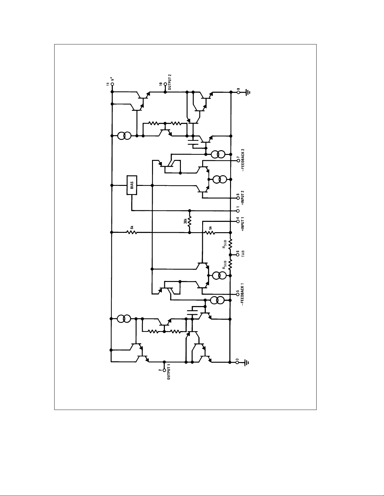
Equivalent Schematic Diagram
TL/H/7933– 2
3
Page 4

Typical Performance Characteristics
Device Dissipation vs
Ambient Temperature
Power Supply Rejection Ratio
(Referred to the Output) vs
Supply Voltage
Average Supply Current vs
Power Output
Power Supply Rejection Ratio
(Referred to the Output) vs
Frequency
Channel Separation (Referred)
to the Output) vs Frequency
Total Harmonic Distortion
vs Frequency
Power Supply Rejection Ratio
(Referred to the Output) vs
Frequency
Channel Separation (Referred)
to the Output) vs Frequency
Total Harmonic Distortion
vs Frequency
Power Dissipation vs
Power Output
Open Loop Gain vs
Frequency
4
Output Swing vs Supply
Voltage
TL/H/7933– 3
Page 5

Typical Applications
Stereo Phonograph Amplifier with Bass Tone Control
Frequency Response of Bass Tone Control
TL/H/7933– 5
5
TL/H/7933– 4
Page 6

Typical Applications (Continued)
Stereo Amplifier with A
e
200
V
Non-Inverting Amplifier Using Split Supply
6
TL/H/7933– 6
TL/H/7933– 7
Page 7

Typical Applications (Continued)
Window Comparator Driving High, Low Lamps
V
IN
a
k
(/4 V
a
to */4 V
a
a
(/4 V
l
*/4 V
Application Hints
The LM2877 is an improved LM377 in typical audio applications. In the LM2877, the internal voltage regulator for the
input stage is generated from the voltage on pin 1. Normally,
the input common-mode range is within
voltage. Nevertheless, the common-mode range can be increased by externally forcing the voltage on pin 1. One way
to do this is to short pin 1 to the positive supply, pin 11.
g
0.7V of this pin 1
Truth Table
High Low
TL/H/7933– 8
Off On
Off Off
On Off
The only special care required with the LM2877 is to limit
the maximum input differential voltage to
g
7V. If this differential voltage is exceeded, the input characteristics may
change.
Figure 1
shows a power op amp application with A
The 100k and 10k resistors set a noise gain of 10 and are
e
V
dictated by amplifier stability. The 10k resistor is bootstrapped by the feedback so the input resistance is dominated by the 1 MX resistor.
1.
FIGURE 1
7
TL/H/7933– 9
Page 8

Physical Dimensions inches (millimeters)
LM2877 Dual 4W Audio Power Amplifier
Order Number LM2877P
See NS Package Number P11A
LIFE SUPPORT POLICY
NATIONAL’S PRODUCTS ARE NOT AUTHORIZED FOR USE AS CRITICAL COMPONENTS IN LIFE SUPPORT
DEVICES OR SYSTEMS WITHOUT THE EXPRESS WRITTEN APPROVAL OF THE PRESIDENT OF NATIONAL
SEMICONDUCTOR CORPORATION. As used herein:
1. Life support devices or systems are devices or 2. A critical component is any component of a life
systems which, (a) are intended for surgical implant support device or system whose failure to perform can
into the body, or (b) support or sustain life, and whose be reasonably expected to cause the failure of the life
failure to perform, when properly used in accordance support device or system, or to affect its safety or
with instructions for use provided in the labeling, can effectiveness.
be reasonably expected to result in a significant injury
to the user.
National Semiconductor National Semiconductor National Semiconductor National Semiconductor National Semiconductores National Semiconductor
Corporation GmbH Japan Ltd. Hong Kong Ltd. Do Brazil Ltda. (Australia) Pty, Ltd.
2900 Semiconductor Drive Livry-Gargan-Str. 10 Sumitomo Chemical 13th Floor, Straight Block, Rue Deputado Lacorda Franco Building 16
P.O. Box 58090 D-82256 F4urstenfeldbruck Engineering Center Ocean Centre, 5 Canton Rd. 120-3A Business Park Drive
Santa Clara, CA 95052-8090 Germany Bldg. 7F Tsimshatsui, Kowloon Sao Paulo-SP Monash Business Park
Tel: 1(800) 272-9959 Tel: (81-41) 35-0 1-7-1, Nakase, Mihama-Ku Hong Kong Brazil 05418-000 Nottinghill, Melbourne
TWX: (910) 339-9240 Telex: 527649 Chiba-City, Tel: (852) 2737-1600 Tel: (55-11) 212-5066 Victoria 3168 Australia
National does not assume any responsibility for use of any circuitry described, no circuit patent licenses are implied and National reserves the right at any time without notice to change said circuitry and specifications.
Fax: (81-41) 35-1 Ciba Prefecture 261 Fax: (852) 2736-9960 Telex: 391-1131931 NSBR BR Tel: (3) 558-9999
Tel: (043) 299-2300 Fax: (55-11) 212-1181 Fax: (3) 558-9998
Fax: (043) 299-2500
 Loading...