

Page 1

LM2841/ LM2842 300 mA/600 mA up to 42V Input Step-Down DC/DC Regulator in Thin SOT-23
LM2841
LM2842
300 mA/600 mA up to 42V Input Step-Down DC/DC
Regulator in Thin SOT-23
General Description
The LM2841 and LM2842 are PWM DC/DC buck (step-down)
regulators. With a wide input range from 4.5V-42V, they are
suitable for a wide range of applications such as power conditioning from unregulated sources. They feature a low
R
(0.9Ω typical) internal switch for maximum efficiency
DSON
(85% typical). Operating frequency is fixed at 550 kHz (X version) and 1.25 MHz (Y version) allowing the use of small
external components while still being able to have low output
voltage ripple. Soft-start can be implemented using the shutdown pin with an external RC circuit allowing the user to tailor
the soft-start time to a specific application.
The LM2842 is optimized for up to 600 mA load currents while
the LM2841 is optimized for up to 300 mA load current. Both
have a 0.765V nominal feedback voltage.
Additional features include: thermal shutdown, VIN under-voltage lockout, and gate drive under-voltage lockout. The
LM2841 and LM2842 are available in a low profile TSOT-6L
package.
Features
Input voltage range of 4.5V to 42V
■
Output current options of 300 mA and 600 mA
■
Feedback pin voltage of 0.765V
■
550 kHz (X) or 1.25 Mhz (Y) switching frequency
■
Low shutdown IQ, 16 µA typical
■
Short circuit protected
■
Internally compensated
■
Soft-start circuitry
■
Small overall solution size (TSOT-6L package)
■
Applications
Battery powered equipment
■
Industrial distributed power applications
■
Portable media players
■
Portable hand held instruments
■
April 2, 2009
Typical Application Circuit
30036702
© 2009 National Semiconductor Corporation 300367 www.national.com
Page 2
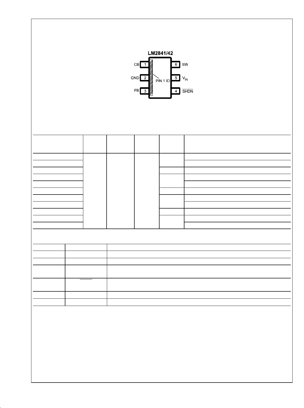
Connection Diagram
LM2841/ LM2842
Top View
NS Package Number MK06A
TSOT 6 Lead
30036704
Ordering Information
Order Number Spec.
LM2841XMK-ADJL
LM2841XMKX-ADJL 3000 Units, Tape and Reel
LM2841YMK-ADJL
LM2841YMKX-ADJL 3000 Units, Tape and Reel
LM2842XMK-ADJL
LM2842XMKX-ADJL 3000 Units, Tape and Reel
LM2842YMK-ADJL
LM2842YMKX-ADJL 3000 Units, Tape and Reel
NOPB TSOT-6 MK06A
Package
Type
NSC
Package
Drawing
Top Mark Supplied As
STFB
STTB
STVB
STXB
1000 Units, Tape and Reel
1000 Units, Tape and Reel
1000 Units, Tape and Reel
1000 Units, Tape and Reel
Pin Descriptions
Pin Name Function
1 CB
2 GND Ground connection.
3 FB
4 SHDN Logic level shutdown input. Pull to GND to disable the device and pull high to enable the device.
5 V
6 SW Power FET output: Connect to inductor, diode, and C
IN
SW FET gate bias voltage. Connect C
Feedback pin: Set feedback voltage divider ratio with V
be in the 100-10K range to avoid input bias errors.
If this function is not used tie to VIN or leave open.
Power input voltage pin: 4.5V to 42V normal operating range.
cap between CB and SW.
BOOT
= VFB (1+(R1/R2)). Resistors should
OUT
cap.
BOOT
www.national.com 2
Page 3
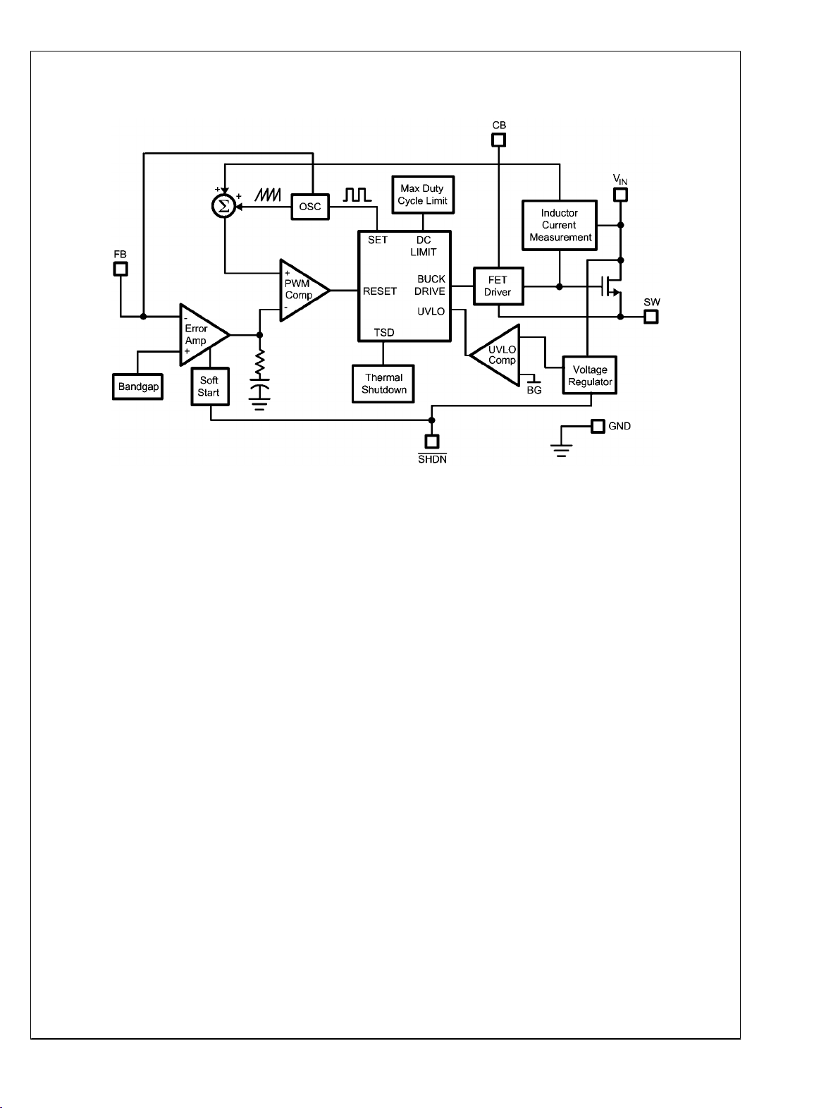
Block Diagram
LM2841/ LM2842
30036703
3 www.national.com
Page 4
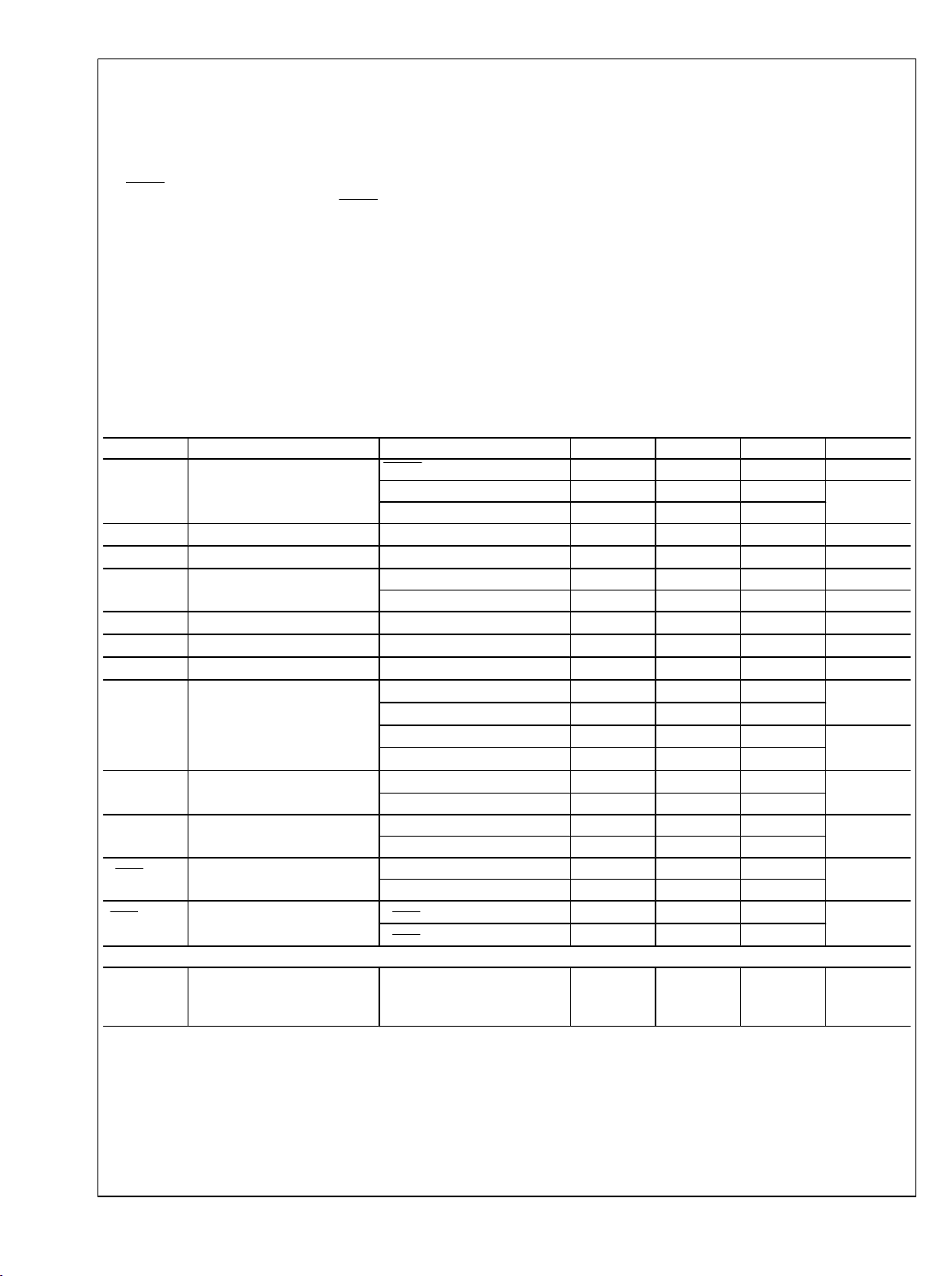
Absolute Maximum Ratings (Note 1)
If Military/Aerospace specified devices are required,
please contact the National Semiconductor Sales Office/
Distributors for availability and specifications.
V
IN
SHDN -0.3V to (VIN+0.3V)
LM2841/ LM2842
SHDN=VIN at 45V max
SW Voltage -0.3V to +45V
CB Voltage above SW Voltage 7V
FB Voltage -0.3V to +5V
Maximum Junction
Temperature
Power Dissipation(Note 2) Internally Limited
-0.3V to +45V
150°C
Lead Temperature 300°C
Vapor Phase (60 sec.) 215°C
Infrared (15 sec.) 220°C
ESD Susceptibility
(Note 3)
Human Body Model 1.5 kV
Operating Conditions
Operating Junction
Temperature Range (Note 4) −40°C to +125°C
Storage Temperature −65°C to +150°C
Input Voltage V
SW Voltage Up to 42V
IN
Electrical Characteristics
Specifications in standard type face are for TJ = 25°C and those with boldface type apply over the full Operating Temperature
Range ( TJ = −40°C to +125°C). Minimum and Maximum limits are guaranteed through test, design, or statistical correlation. Typical
values represent the most likely parametric norm at TJ = +25°C, and are provided for reference purposes only. Unless otherwise
stated the following conditions apply: VIN = 12V.
Symbol Parameter Conditions Min(Note 4) Typ(Note 5) Max(Note 4) Units
I
Q
R
DSON
I
LSW
I
CL
I
FB
V
FB
t
MIN
f
SW
D
MAX
V
UVP
V
SHDN
I
SHDN
THERMAL SPECIFICATIONS
R
θJA
Quiescent current SHDN = 0V 16 40 µA
Device On, Not Switching 1.30 1.75
Device On, No Load 1.35 1.85
Switch ON resistance (Note 6) 0.9 1.6
Switch leakage current VIN = 42V
0.0 0.5 µA
Switch current limit LM2842 (Note 7) 1.15 A
LM2841 (Note 7) 525 mA
Feedback pin bias current LM2841/42 (Note 8)
FB Pin reference voltage
0.747 0.765 0.782 V
Minimum ON time
Switching frequency LM2841/42X, VFB = 0.5V
325 550 750
LM2841/42X, VFB = 0V
LM2841/42Y, VFB = 0.5V
0.95 1.25 1.50
LM2841/42Y, VFB = 0V
100 ns
140
0.1 1.0 µA
0.35
Maximum duty cycle LM2841/42X 88 94
LM2841/42Y 81 87
Undervoltage lockout
thresholds
On threshold 4.4 3.7
Off threshold 3.5 3.25
Shutdown threshold Device on 2.3 1.0
Device off 0.9 0.3
Shutdown pin input bias
current
Junction-to-Ambient Thermal
Resistance, TSOT-6L
V
= 2.3V (Note 8)
SHDN
V
= 0V
SHDN
(Note 9)
0.05 1.5
0.02 1.5
121 °C/W
Package
4.5V to 42V
mA
Ω
kHz
MHz
%
V
V
µA
www.national.com 4
Page 5

Note 1: Absolute maximum ratings are limits beyond which damage to the device may occur. Operating Ratings are conditions for which the device is intended
to be functional, but device parameter specifications may not be guaranteed. For guaranteed specifications and test conditions, see the Electrical Characteristics.
Note 2: The maximum allowable power dissipation is a function of the maximum junction temperature, TJ(MAX), the junction-to-ambient thermal resistance,
θJA, and the ambient temperature, TA. The maximum allowable power dissipation at any ambient temperature is calculated using: PD (MAX) = (T
θJA. Exceeding the maximum allowable power dissipation will cause excessive die temperature, and the regulator will go into thermal shutdown. Internal thermal
shutdown circuitry protects the device from permanent damage. Thermal shutdown engages at TJ=175°C (typ.) and disengages at TJ=155°C (typ).
Note 3: Human Body Model, applicable std. JESD22-A114-C.
Note 4: All limits guaranteed at room temperature (standard typeface) and at temperature extremes (bold typeface). All room temperature limits are 100%
production tested. All limits at temperature extremes are guaranteed via correlation using standard Statistical Quality Control (SQC) methods. All limits are used
to calculate Average Outgoing Quality Level (AOQL).
Note 5: Typical numbers are at 25°C and represent the most likely norm.
Note 6: Includes the bond wires, R
Note 7: Current limit at 0% duty cycle.
Note 8: Bias currents flow into pin.
Note 9: All numbers apply for packages soldered directly onto a 3" x 3" PC board with 2 oz. copper on 4 layers in still air in accordance to JEDEC standards.
Thermal resistance varies greatly with layout, copper thickness, number of layers in PCB, power distribution, number of thermal vias, board size, ambient
temperature, and air flow.
from VIN pin to SW pin.
DSON
J(MAX)
− TA)/
LM2841/ LM2842
5 www.national.com
Page 6

Typical Performance Characteristics
LM2841/ LM2842
Efficiency vs. Load Current
(LM2842X, V
OUT
= 3.3V)
Efficiency vs. Load Current
(LM2841X, V
OUT
= 8V)
30036718
Efficiency vs. Load Current
(LM2841X, V
OUT
= 3.3V)
30036719
Switching Frequency vs. Temperature
(X version)
30036720
Input UVLO Voltage vs. Temperature
30036767
www.national.com 6
30036766
Switch Current Limit vs. SHDN Pin Voltage
(Soft-start Implementation, LM2841)
30036768
Page 7
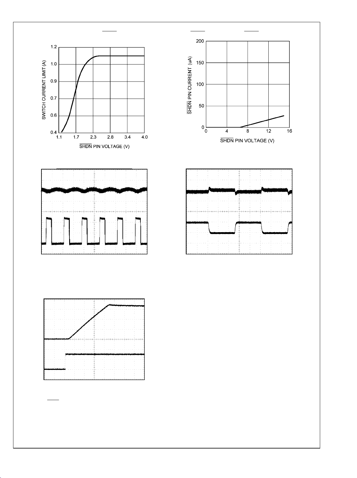
LM2841/ LM2842
Switch Current Limit vs. SHDN Pin Voltage
(Soft-start Implementation, LM2842)
30036721
Switching Node and Output Voltage Waveforms
SHDN Pin Current vs. SHDN Pin Voltage
30036769
Load Transient Waveforms
VIN = 12V, V
Top trace: V
= 3.3V, I
OUT
, 10 mV/div, AC Coupled
OUT
= 200 mA
OUT
Bottom trace: SW, 5V/div, DC Coupled
T = 400 ns/div
Start-up Waveform
VIN = 12V, V
Top trace: V
Bottom trace: SHDN, 2V/div, DC Coupled
T = 40 µs/div
= 3.3V, I
OUT
OUT
OUT
, 1V/div, DC Coupled
= 50 mA
30036770
30036772
VIN = 12V, V
Top trace: V
Bottom trace: I
T = 200 µs/div
= 3.3V, I
OUT
, 20 mV/div, AC Coupled
OUT
, 100 mA/div, DC Coupled
OUT
= 300 mA to 200 mA to 300 mA
OUT
30036771
7 www.national.com
Page 8

Operation
PROTECTION
The LM2841/42 has dedicated protection circuitry running
during normal operation to protect the IC. The thermal shutdown circuitry turns off the power device when the die temperature reaches excessive levels. The UVLO comparator
LM2841/ LM2842
protects the power device during supply power startup and
shutdown to prevent operation at voltages less than the minimum input voltage. A gate drive (CB) under-voltage lockout
is included to guarantee that there is enough gate drive voltage to drive the MOSFET before the device tries to start
switching. The LM2841/42 also features a shutdown mode
decreasing the supply current to approximately 16 µA.
CONTINUOUS CONDUCTION MODE
The LM2841/42 contains a current-mode, PWM buck regulator. A buck regulator steps the input voltage down to a lower
output voltage. In continuous conduction mode (when the inductor current never reaches zero at steady state), the buck
regulator operates in two cycles. The power switch is connected between VIN and SW. In the first cycle of operation the
transistor is closed and the diode is reverse biased. Energy
is collected in the inductor and the load current is supplied by
C
and the rising current through the inductor. During the
OUT
second cycle the transistor is open and the diode is forward
biased due to the fact that the inductor current cannot instantaneously change direction. The energy stored in the inductor
is transferred to the load and output capacitor. The ratio of
these two cycles determines the output voltage. The output
voltage is defined approximately as: D=V
D) where D is the duty cycle of the switch. D and D' will be
required for design calculations.
DESIGN PROCEDURE
This section presents guidelines for selecting external components.
SETTING THE OUTPUT VOLTAGE
The output voltage is set using the feedback pin and a resistor
divider connected to the output as shown on the front page
schematic. The feedback pin voltage is 0.762V, so the ratio
of the feedback resistors sets the output voltage according to
the following equation: V
R2 will be given as 100Ω-10 kΩ for a starting value. To solve
for R1 given R2 and V
=0.765V(1+(R1/R2)) Typically
OUT
use R1=R2((V
OUT
INPUT CAPACITOR
A low ESR ceramic capacitor (CIN) is needed between the
VIN pin and GND pin. This capacitor prevents large voltage
transients from appearing at the input. Use a 2.2 µF-10 µF
value with X5R or X7R dielectric. Depending on construction,
a ceramic capacitor’s value can decrease up to 50% of its
nominal value when rated voltage is applied. Consult with the
capacitor manufacturer's data sheet for information on capacitor derating over voltage and temperature.
INDUCTOR SELECTION
The most critical parameters for the inductor are the inductance, peak current, and the DC resistance. The inductance
is related to the peak-to-peak inductor ripple current, the input
and the output voltages.
OUT/VIN
/0.765V)-1).
OUT
and D’ = (1-
A higher value of ripple current reduces inductance, but increases the conductance loss, core loss, and current stress
for the inductor and switch devices. It also requires a bigger
output capacitor for the same output voltage ripple requirement. A reasonable value is setting the ripple current to be
30% of the DC output current. Since the ripple current increases with the input voltage, the maximum input voltage is
always used to determine the inductance. The DC resistance
of the inductor is a key parameter for the efficiency. Lower DC
resistance is available with a bigger winding area. A good
tradeoff between the efficiency and the core size is letting the
inductor copper loss equal 2% of the output power. See
AN-1197 for more information on selecting inductors. A good
starting point for most applications is a 10 µH to 22 µH with
1.1A or greater current rating for the LM2842 or a 0.7A or
greater current rating for the LM2841. Using such a rating will
enable the LM2841/42 to current limit without saturating the
inductor. This is preferable to the LM2841/42 going into thermal shutdown mode and the possibility of damaging the inductor if the output is shorted to ground or other longterm
overload.
OUTPUT CAPACITOR
The selection of C
output voltage ripple. The output ripple in the constant frequency, PWM mode is approximated by: V
(ESR+(1/8fSWC
nant role in determining the voltage ripple. Low ESR ceramic
is driven by the maximum allowable
OUT
= I
)) The ESR term usually plays the domi-
OUT
RIPPLE
RIPPLE
capacitors are recommended. Capacitors in the range of 22
µF-100 µF are a good starting point with an ESR of 0.1Ω or
less.
BOOTSTRAP CAPACITOR
A 0.15 µF ceramic capacitor or larger is recommended for the
bootstrap capacitor (C
voltage is less than twice the output voltage a larger capacitor
). For applications where the input
BOOT
is recommended, generally 0.15 µF to 1 µF to ensure plenty
of gate drive for the internal switches and a consistently low
R
.
DSON
SOFT-START COMPONENTS
The LM2841/42 has circuitry that is used in conjunction with
the SHDN
pin to limit the inrush current on start-up of the DC/
DC switching regulator. The SHDN pin in conjunction with a
RC filter is used to tailor the soft-start for a specific application.
When a voltage applied to the SHDN pin is between 0V and
up to 2.3V it will cause the cycle by cycle current limit in the
power stage to be modulated for minimum current limit at 0V
up to the rated current limit at 2.3V. Thus controlling the output
rise time and inrush current at startup. The resistor value
should be selected so the current sourced into the SHDN pin
will be greater then the leakage current of the SHDN pin (1.5
µA ) when the voltage at SHDN is equal or greater then 2.3V.
SHUTDOWN OPERATION
The SHDN pin of the LM2841/42 is designed so that it may
be controlled using 2.3V or higher logic signals. If the shutdown function is not to be used the SHDN pin may be tied to
VIN. The maximum voltage to the SHDN pin should not exceed 42V. If the use of a higher voltage is desired due to
system or other constraints it may be used, however a 100
kΩ or larger resistor is recommended between the applied
voltage and the SHDN pin to protect the device.
www.national.com 8
SCHOTTKY DIODE
The breakdown voltage rating of the diode (D1) is preferred
to be 25% higher than the maximum input voltage. The cur-
Page 9

LM2841/ LM2842
rent rating for the diode should be equal to the maximum
output current for best reliability in most applications. In cases
where the input voltage is much greater than the output voltage the average diode current is lower. In this case it is
possible to use a diode with a lower average current rating,
approximately (1-D)I
should be higher than the maximum load current. A 0.5A to
, however the peak current rating
OUT
1A rated diode is a good starting point.
LAYOUT CONSIDERATIONS
To reduce problems with conducted noise pick up, the ground
side of the feedback network should be connected directly to
the GND pin with its own connection. The feedback network,
resistors R1 and R2, should be kept close to the FB pin, and
away from the inductor to minimize coupling noise into the
feedback pin. The input bypass capacitor CIN must be placed
close to the VIN pin. This will reduce copper trace resistance
which effects input voltage ripple of the IC. The inductor L1
should be placed close to the SW pin to reduce magnetic and
electrostatic noise. The output capacitor, C
placed close to the junction of L1 and the diode D1. The L1,
D1, and C
conducted and radiated noise and increase overall efficiency.
trace should be as short as possible to reduce
OUT
The ground connection for the diode, CIN, and C
be as small as possible and tied to the system ground plane
in only one spot (preferably at the C
imize conducted noise in the system ground plane. For more
ground point) to min-
OUT
should be
OUT
OUT
should
detail on switching power supply layout considerations see
Application Note AN-1149: Layout Guidelines for Switching
Power Supplies.
9 www.national.com
Page 10
Application Information
LM2841/ LM2842
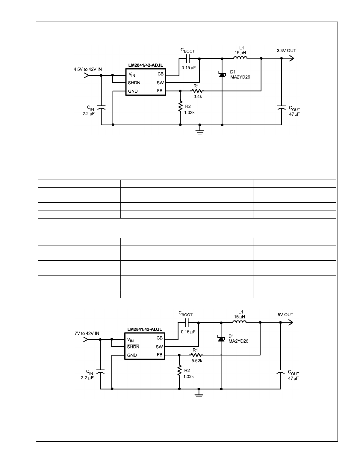
FIGURE 1. Application Circuit, 3.3V Output
Some Recommended Inductors (Others May Be Used)
Manufacturer Inductor Contact Information
Coilcraft LPS4018, DO1608C, DO3308, and LPO2506 series www.coilcraft.com
MuRata LQH55D and LQH66S series www.murata.com
Coiltronics MP2 and MP2A series www.cooperbussman.com
30036705
800-3222645
Some Recommended Input And Output Capacitors (Others May Be Used)
Manufacturer Capacitor Contact Information
Vishay Sprague 293D, 592D, and 595D series tantalum www.vishay.com
407-324-4140
Taiyo Yuden High capacitance MLCC ceramic www.t-yuden.com
408-573-4150
Cornell Dubilier
MuRata High capacitance MLCC ceramic www.murata.com
ESRD seriec Polymer Aluminum Electrolytic
SPV and AFK series V-chip series
www.cde.com
30036708
FIGURE 2. Application Circuit, 5V Output
www.national.com 10
Page 11
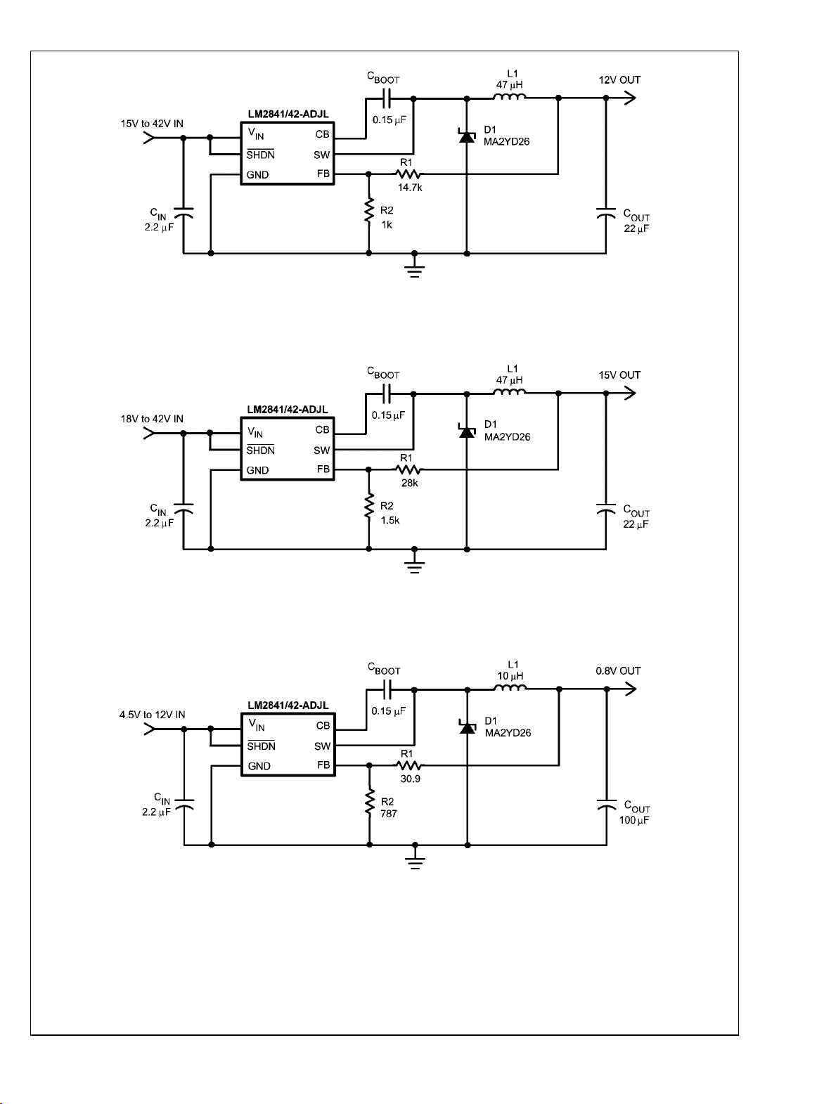
FIGURE 3. Application Circuit, 12V Output
LM2841/ LM2842
30036709
FIGURE 4. Application Circuit, 15V Output
FIGURE 5. Application Circuit, 0.8V Output
30036716
30036717
11 www.national.com
Page 12

Physical Dimensions inches (millimeters) unless otherwise noted
LM2841/ LM2842
For Ordering, Refer to Ordering Information Table
TSOT 6 Pin Package (MK)
NS Package Number MK06A
www.national.com 12
Page 13

Notes
LM2841/ LM2842
13 www.national.com
Page 14
Notes
For more National Semiconductor product information and proven design tools, visit the following Web sites at:
Products Design Support
Amplifiers www.national.com/amplifiers WEBENCH® Tools www.national.com/webench
Audio www.national.com/audio App Notes www.national.com/appnotes
Clock and Timing www.national.com/timing Reference Designs www.national.com/refdesigns
Data Converters www.national.com/adc Samples www.national.com/samples
Interface www.national.com/interface Eval Boards www.national.com/evalboards
LVDS www.national.com/lvds Packaging www.national.com/packaging
Power Management www.national.com/power Green Compliance www.national.com/quality/green
Switching Regulators www.national.com/switchers Distributors www.national.com/contacts
LDOs www.national.com/ldo Quality and Reliability www.national.com/quality
LED Lighting www.national.com/led Feedback/Support www.national.com/feedback
Voltage Reference www.national.com/vref Design Made Easy www.national.com/easy
PowerWise® Solutions www.national.com/powerwise Solutions www.national.com/solutions
Serial Digital Interface (SDI) www.national.com/sdi Mil/Aero www.national.com/milaero
Temperature Sensors www.national.com/tempsensors SolarMagic™ www.national.com/solarmagic
Wireless (PLL/VCO) www.national.com/wireless Analog University® www.national.com/AU
THE CONTENTS OF THIS DOCUMENT ARE PROVIDED IN CONNECTION WITH NATIONAL SEMICONDUCTOR CORPORATION
(“NATIONAL”) PRODUCTS. NATIONAL MAKES NO REPRESENTATIONS OR WARRANTIES WITH RESPECT TO THE ACCURACY
OR COMPLETENESS OF THE CONTENTS OF THIS PUBLICATION AND RESERVES THE RIGHT TO MAKE CHANGES TO
SPECIFICATIONS AND PRODUCT DESCRIPTIONS AT ANY TIME WITHOUT NOTICE. NO LICENSE, WHETHER EXPRESS,
IMPLIED, ARISING BY ESTOPPEL OR OTHERWISE, TO ANY INTELLECTUAL PROPERTY RIGHTS IS GRANTED BY THIS
DOCUMENT.
TESTING AND OTHER QUALITY CONTROLS ARE USED TO THE EXTENT NATIONAL DEEMS NECESSARY TO SUPPORT
NATIONAL’S PRODUCT WARRANTY. EXCEPT WHERE MANDATED BY GOVERNMENT REQUIREMENTS, TESTING OF ALL
PARAMETERS OF EACH PRODUCT IS NOT NECESSARILY PERFORMED. NATIONAL ASSUMES NO LIABILITY FOR
APPLICATIONS ASSISTANCE OR BUYER PRODUCT DESIGN. BUYERS ARE RESPONSIBLE FOR THEIR PRODUCTS AND
APPLICATIONS USING NATIONAL COMPONENTS. PRIOR TO USING OR DISTRIBUTING ANY PRODUCTS THAT INCLUDE
NATIONAL COMPONENTS, BUYERS SHOULD PROVIDE ADEQUATE DESIGN, TESTING AND OPERATING SAFEGUARDS.
EXCEPT AS PROVIDED IN NATIONAL’S TERMS AND CONDITIONS OF SALE FOR SUCH PRODUCTS, NATIONAL ASSUMES NO
LIABILITY WHATSOEVER, AND NATIONAL DISCLAIMS ANY EXPRESS OR IMPLIED WARRANTY RELATING TO THE SALE
AND/OR USE OF NATIONAL PRODUCTS INCLUDING LIABILITY OR WARRANTIES RELATING TO FITNESS FOR A PARTICULAR
PURPOSE, MERCHANTABILITY, OR INFRINGEMENT OF ANY PATENT, COPYRIGHT OR OTHER INTELLECTUAL PROPERTY
RIGHT.
LIFE SUPPORT POLICY
NATIONAL’S PRODUCTS ARE NOT AUTHORIZED FOR USE AS CRITICAL COMPONENTS IN LIFE SUPPORT DEVICES OR
SYSTEMS WITHOUT THE EXPRESS PRIOR WRITTEN APPROVAL OF THE CHIEF EXECUTIVE OFFICER AND GENERAL
COUNSEL OF NATIONAL SEMICONDUCTOR CORPORATION. As used herein:
Life support devices or systems are devices which (a) are intended for surgical implant into the body, or (b) support or sustain life and
whose failure to perform when properly used in accordance with instructions for use provided in the labeling can be reasonably expected
to result in a significant injury to the user. A critical component is any component in a life support device or system whose failure to perform
can be reasonably expected to cause the failure of the life support device or system or to affect its safety or effectiveness.
National Semiconductor and the National Semiconductor logo are registered trademarks of National Semiconductor Corporation. All other
brand or product names may be trademarks or registered trademarks of their respective holders.
Copyright© 2009 National Semiconductor Corporation
For the most current product information visit us at www.national.com
National Semiconductor
Americas Technical
Support Center
LM2841/ LM2842 300 mA/600 mA up to 42V Input Step-Down DC/DC Regulator in Thin SOT-23
www.national.com
Email: [email protected]
Tel: 1-800-272-9959
National Semiconductor Europe
Technical Support Center
Email: [email protected]
National Semiconductor Asia
Pacific Technical Support Center
Email: [email protected]
National Semiconductor Japan
Technical Support Center
Email: [email protected]
 Loading...