

Page 1
LM2725/LM2726
High Speed Synchronous MOSFET Drivers
General Description
The LM2725/LM2726 is a family of dual MOSFET drivers
that can drive both the top MOSFET and bottom MOSFET in
a push-pull structure simultaneously. It takes a logic level
PWM input and splits it into two complimentary signals with
a typical 20ns dead time in between. The built-in
shoot-through protection circuitry prevents the top and bottom FETs from turning on simultaneously. With a bias voltage of 5V, the peak sourcing and sinking current for each
driver of the LM2725 is about 1.2AandthatoftheLM2726is
about 3A. In an SO-8 package, each driver is able to handle
50mA average current. Input UVLO
(Under-Voltage-Lock-Out) ensures that all the driver outputs
stay low until the supply rail exceeds the power-on threshold
during system power on, or after the supply rail drops below
power-on threshold by a specified hysteresis during system
power down. The cross-conduction protection circuitry detects both the driver outputs and will not turn on a driver until
the other driver output is low. The top gate bias voltage
needed by the top MOSFET can be obtained through an
external bootstrap structure. Minimum pulse width is as low
as 55ns.
Features
n High peak output current
n Adaptive shoot-through protection
n 36V SW pin absolute maximum voltage
n Input Under-Voltage-Lock-Out
n Typical 20ns internal delay
n Plastic 8-pin SO package
Applications
n High Current DC/DC Power Supplies
n High Input Voltage Switching Regulators
n Microprocessors
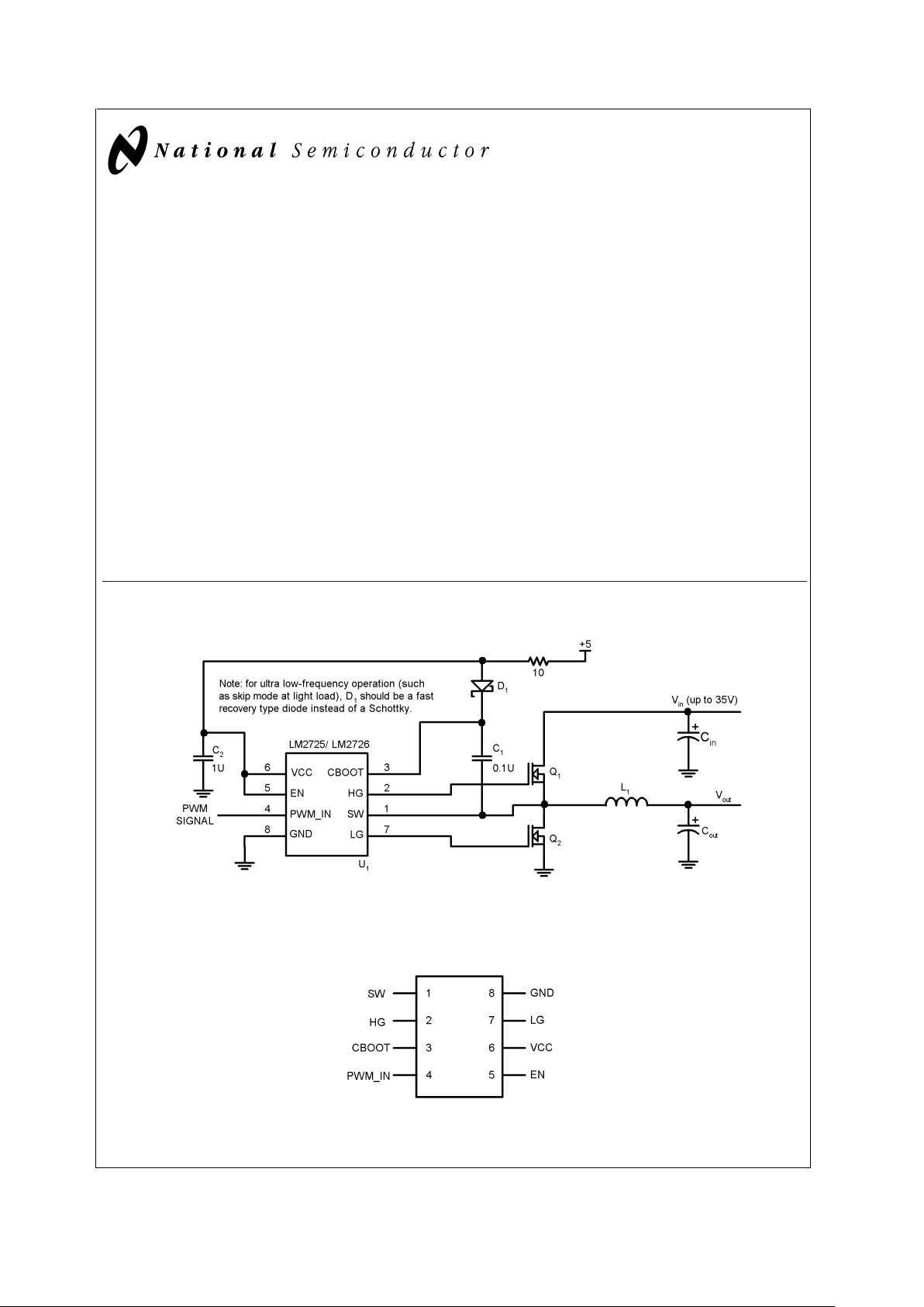
Typical Application
Connection Diagram
DS200072-1
8-Lead Small Outline Package
DS200072-2
Top View
November 2000
LM2725/LM2726 High Speed Synchronous MOSFET Drivers
© 2000 National Semiconductor Corporation DS200072 www.national.com
Page 2

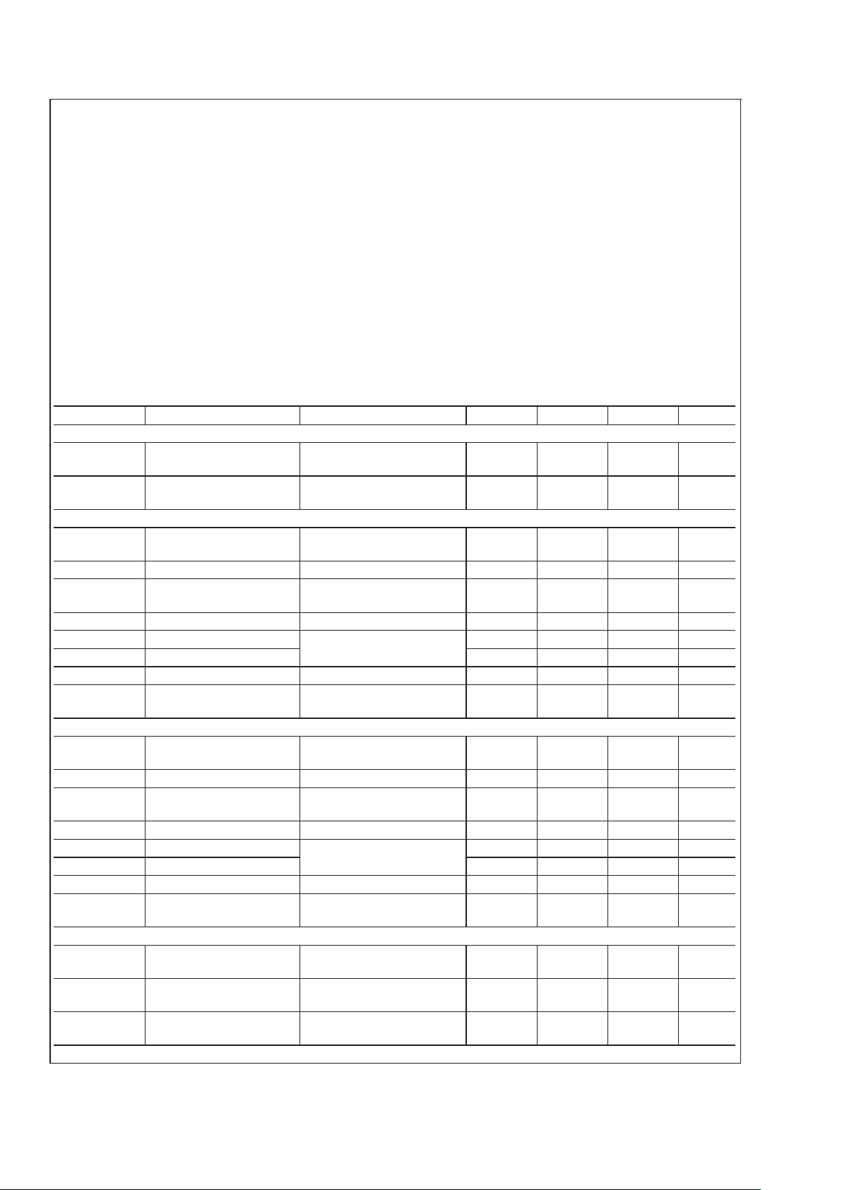
Ordering Information
Order Number Package Type NSC Package Drawing Supplied As
LM2725 LM2725M
M08A
95 Units/Rail
LM2725MX 2500 Units/Reel
LM2726 LM2726M 95 Units/Rail
LM2726MX 2500 Units/Reel
Pin Description
Pin Name Function
1 SW Top driver return. Should be connected to the common node of
top and bottom FETs
2 HG Top gate drive output
3 CBOOT Bootstrap. Accepts a bootstrap voltage for powering the high-side
driver
4 PWM_IN Accepts a 5V-logic control signal
5 EN Chip Enable
6 VCC Connect to +5V supply
7 LG Bottom gate drive output
8 GND Ground
Block Diagram
DS200072-4
LM2725/LM2726
www.national.com 2
Page 3
Absolute Maximum Ratings (Note 1)
If Military/Aerospace specified devices are required,
please contact the NationalSemiconductorSales Office/
Distributors for availability and specifications.
VCC 7.5V
CBOOT 42V
CBOOT to SW 8V
SW to PGND 36V
Junction Temperature +150˚C
Power Dissipation
(Note 2) 720mW
Storage Temperature −65˚ to 150˚C
ESD Susceptibility
Human Body Model (Note 3) 1 kV
Soldering Time, Temperature 10sec., 300˚C
Operating Ratings (Note 1)
VCC 4V to 7V
Junction Temperature Range 0˚ to 125˚C
Electrical Characteristics
LM2725
VCC = CBOOT = 5V, SW = GND = 0V, unless otherwise specified. Typicals and limits appearing in plain type apply for T
A
=TJ= +25˚C. Limits appearing in boldface type apply over the entire operating temperature range.
Symbol Parameter Condition Min Typ Max Units
POWER SUPPLY
I
q_op
Operating Quiescent
Current
PWM_IN = 0V
180 250
µA
I
q_sd
Shutdown Quiescent
Current
EN = 0V, PWM_IN = 0V
0.5 15 µA
TOP DRIVER
Peak Pull-Up Current Test Circuit 1, V
bias
= 5V,
R = 0.1Ω
1.2 A
Pull-Up Rds_on I
CBOOT=IHG
= 0.7A 2.4 Ω
Peak Pull-down Current Test Circuit 2, V
bias
= 5V,
R = 0.1Ω
−1.0 A
Pull-down Rds_on I
SW=IHG
= 0.7A 1.4 Ω
t
4
Rise Time Timing Diagram, C
LOAD
=
3.3nF
17 ns
t
6
Fall Time 10 ns
t
3
Pull-Up Dead Time Timing Diagram 23 ns
t
5
Pull-Down Delay Timing Diagram, from
PWM_IN Falling Edge
21 ns
BOTTOM DRIVER
Peak Pull-Up Current Test Circuit 3, V
bias
= 5V,
R = 0.1Ω
1.2 A
Pull-up Rds_on I
VCC=ILG
= 0.7A 2.6 Ω
Peak Pull-down Current Test Circuit 4, V
bias
= 5V,
R = 0.1Ω
−2 A
Pull-down Rds_on I
GND=ILG
= 0.7A 0.65 Ω
t
8
Rise Time Timing Diagram, C
LOAD
=
3.3nF
18 ns
t
2
Fall Time 6 ns
t
7
Pull-up Dead Time Timing Diagram 28 ns
t
1
Pull-down Delay Timing Diagram, from
PWM_IN Rising Edge
15 ns
LOGIC
V
uvlo_up
Power On Threshold VCC rises from 0V toward
5V
3.0 V
V
uvlo_dn
Under-Voltage-Lock-Out
Threshold
2.5 V
V
uvlo_hys
Under-Voltage-Lock-Out
Hysteresis
0.5 V
LM2725/LM2726
www.national.com3
Page 4

Electrical Characteristics
LM2725
(Continued)
VCC = CBOOT = 5V, SW = GND = 0V, unless otherwise specified. Typicals and limits appearing in plain type apply for T
A
=TJ= +25˚C. Limits appearing in boldface type apply over the entire operating temperature range.
Symbol Parameter Condition Min Typ Max Units
LOGIC
V
IH_EN
EN Pin High Input 2.4 V
V
IL_EN
EN Pin Low Input 0.8 V
I
leak_EN
EN Pin Leakage Current EN = VCC = 5V −2 2
µA
VCC = 5V, EN = 0V −2 2
t
on_min
Minimum Positive Input
Pulse Width
(Note 4)
55
ns
t
off_min
Minimum Negative Input
Pulse Width
(Note 5)
55
V
IH_PWM
PWM_IN High Level
Input Voltage
When PWM_IN pin goes
high from 0V
2.4
V
V
IL_PWM
PWM_IN Low Level
Input Voltage
When PWM_IN pin goes
low from 5V
0.8
Electrical Characteristics
LM2726
VCC = CBOOT = 5V, SW = GND = 0V, unless otherwise specified. Typicals and limits appearing in plain type apply for T
A
=TJ= +25˚C. Limits appearing in boldface type apply over the entire operating temperature range.
Symbol Parameter Condition Min Typ Max Units
POWER SUPPLY
I
q_op
Operating Quiescent
Current
PWM_IN = 0V
185 250
µA
I
q_sd
Shutdown Quiescent
Current
EN = 0V, PWM_IN = 0V
0.5 15 µA
TOP DRIVER
Peak Pull-Up Current Test Circuit 1, V
bias
= 5V,
R = 0.1Ω
3.0 A
Pull-Up Rds_on I
CBOOT=IHG
= 1.0A 1.2 Ω
Peak Pull-down Current Test Circuit 2, V
bias
= 5V,
R = 0.1Ω
−3.2 A
Pull-down Rds_on I
SW=IHG
= 1.0A 0.5 Ω
t
4
Rise Time Timing Diagram, C
LOAD
=
3.3nF
17 ns
t
6
Fall Time 12 ns
t
3
Pull-Up Dead Time Timing Diagram 19 ns
t
5
Pull-Down Delay Timing Diagram, from
PWM_IN from Falling Edge
27 ns
BOTTOM DRIVER
Peak Pull-Up Current Test Circuit 3, V
bias
= 5V,
R = 0.1Ω
3.2 A
Pull-up Rds_on I
VCC=ILG
= 1.0A 1.1 Ω
Peak Pull-down Current Test Circuit 4, V
bias
= 5V,
R = 0.1Ω
−3.2 A
Pull-down Rds_on I
GND=ILG
= 1.0A 0.6 Ω
t
8
Rise Time Timing Diagram, C
LOAD
=
3.3nF
17 ns
t
2
Fall Time 14 ns
t
7
Pull-up Dead Time Timing Diagram 12 ns
LM2725/LM2726
www.national.com 4
Page 5

Electrical Characteristics
LM2726
(Continued)
VCC = CBOOT = 5V, SW = GND = 0V, unless otherwise specified. Typicals and limits appearing in plain type apply for T
A
=TJ= +25˚C. Limits appearing in boldface type apply over the entire operating temperature range.
Symbol Parameter Condition Min Typ Max Units
BOTTOM DRIVER
t
1
Pull-down Delay Timing Diagram, from
PWM_IN Rising Edge
13 ns
LOGIC
V
uvlo_up
Power On Threshold VCC rises from 0V toward
5V
2.8 V
V
uvlo_dn
Under-Voltage-Lock-Out
Threshold
2.5 V
V
uvlo_hys
Under-Voltage-Lock-Out
Hysteresis
0.3 V
V
IH_EN
EN Pin High Input 2.4 V
V
IL_EN
EN Pin Low Input 0.25 V
I
leak_EN
EN Pin Leakage Current EN = VCC = 5V −2 2
µA
VCC = 5V, EN = 0V −2 2
t
on_min
Minimum Positive Input
Pulse Width
(Note 4)
55
ns
t
off_min
Minimum Negative Input
Pulse Width
(Note 5)
55
V
IH_PWM
PWM_IN High Level
Input Voltage
When PWM_IN pin goes
high from 0V
2.4
V
V
IL_PWM
PWM_IN Low Level
Input Voltage
When PWM_IN pin goes
low from 5V
0.25
Note 1: Absolute Maximum Ratings are limits beyond which damage to the device may occur. Operating ratings are conditions under which the device operates
correctly. Operating Ratings do not imply guaranteed performance limits.
Note 2: Maximum allowable power dissipation is a function of the maximum junction temperature, T
JMAX
, the junction-to-ambient thermal resistance, θJA, and the
ambient temperature, T
A
. The maximum allowable power dissipation at any ambient temperature is calculated using: P
MAX
=(T
JMAX-TA
)/θJA. The junction-to-
ambient thermal resistance, θ
JA
, for LM2725/LM2726 is 172˚C/W. For a T
JMAX
of 150˚C and TAof 25˚C, the maximum allowable power dissipation is 0.7W.
Note 3: ESD machine model susceptibility is 100V.
Note 4: If after a rising edge, a falling edge occurs sooner than the specified value, the IC may intermittently fail to turn on the bottom gate when the top gate isoff.
As the falling edge occurs sooner and sooner, the driver may start to ignore the pulse and produce no output.
Note 5: If after a falling edge, a rising edge occurs sooner than the specified value, the IC may intermittently fail to turn on the top gate when the bottom gate isoff.
As the rising edge occurs sooner and sooner, the driver may start to ignore the pulse and produce no output.
LM2725/LM2726
www.national.com5
Page 6

Timing Diagram
DS200072-3
LM2725/LM2726
www.national.com 6
Page 7

Test Circuits
DS200072-5
Test Circuit 1
DS200072-6
Test Circuit 2
DS200072-7
Test Circuit 3
DS200072-8
Test Circuit 4
LM2725/LM2726
www.national.com7
Page 8

Typical Waveforms
DS200072-13
FIGURE 1. Switching Waveforms of Test Circuit
DS200072-14
FIGURE 2. When Input Goes High
DS200072-15
FIGURE 3. When Input Goes Low
DS200072-16
FIGURE 4. Minimum Positive Pulse
LM2725/LM2726
www.national.com 8
Page 9

Physical Dimensions inches (millimeters) unless otherwise noted
LIFE SUPPORT POLICY
NATIONAL’S PRODUCTS ARE NOT AUTHORIZED FOR USE AS CRITICAL COMPONENTS IN LIFE SUPPORT
DEVICES OR SYSTEMS WITHOUT THE EXPRESS WRITTEN APPROVAL OF THE PRESIDENT AND GENERAL
COUNSEL OF NATIONAL SEMICONDUCTOR CORPORATION. As used herein:
1. Life support devices or systems are devices or
systems which, (a) are intended for surgical implant
into the body, or (b) support or sustain life, and
whose failure to perform when properly used in
accordance with instructions for use provided in the
labeling, can be reasonably expected to result in a
significant injury to the user.
2. A critical component is any component of a life
support device or system whose failure to perform
can be reasonably expected to cause the failure of
the life support device or system, or to affect its
safety or effectiveness.
National Semiconductor
Corporation
Americas
Tel: 1-800-272-9959
Fax: 1-800-737-7018
Email: support@nsc.com
National Semiconductor
Europe
Fax: +49 (0) 180-530 85 86
Email: europe.support@nsc.com
Deutsch Tel: +49 (0) 69 9508 6208
English Tel: +44 (0) 870 24 0 2171
Français Tel: +33 (0) 1 41 91 8790
National Semiconductor
Asia Pacific Customer
Response Group
Tel: 65-2544466
Fax: 65-2504466
Email: ap.support@nsc.com
National Semiconductor
Japan Ltd.
Tel: 81-3-5639-7560
Fax: 81-3-5639-7507
www.national.com
8-Lead Small Outline Package
NS Package Number M08A
LM2725/LM2726 High Speed Synchronous MOSFET Drivers
National does not assume any responsibility for use of any circuitry described, no circuit patent licenses are implied and National reserves the right at any time without notice to change said circuitry and specifications.
 Loading...