

Page 1

December 2001
LM2722
High Speed Synchronous/Asynchronous MOSFET Driver
General Description
The LM2722, part of the LM2726 family, is designed to be
used with multi-phase controllers. This part differs from the
LM2726 by changing the functionality of the SYNC_EN pin
from a whole chip enable to a low side MOSFET enable. As
a result, the SYNC_EN pin now provides control between
Synchronous and Asynchronous operations. Having this
control can be advantageous in portable systems since
Asynchronous operations can be more efficient at very light
loads.
The LM2722 drives both top and bottom MOSFETs in a
push-pull structure simultaneously. It takes a logic level
PWM input and splits it into two complimentary signals with
a typical 20ns dead time in between. The built-in
cross-conduction protection circuitry prevents the top and
bottom FETs from turning on simultaneously. The
cross-conduction protection circuitry detects both the driver
outputs and will not turn on a driver until the other driver
output is low. With a bias voltage of 5V, the peak sourcing
and sinking current for each driver of the LM2722 is typically
3A. In an SO-8 package, each driver is able to handle 50mA
average current. Input UVLO (Under-Voltage-Lock-Out)
forces both driver outputs low to ensure proper power-up
and power-down operation. The gate drive bias voltage
needed by the high side MOSFET is obtained through an
external bootstrap. Minimum pulse width is as low as 55ns.
Features
n Synchronous or Asynchronous Operation
n Adaptive shoot-through protection
n Input Under-Voltage-Lock-Out
n Typical 20ns internal delay
n Plastic 8-pin SO package
Applications
n Driver for LM2723 Intel Mobile Northwood CPU core
power supply.
n High Current DC/DC Power Supplies
n High Input Voltage Switching Regulators
n Fast Transient Microprocessors
LM2722 High Speed Synchronous/Asynchronous MOSFET Driver
Typical Application
Note: National is an Intel Mobile Voltage Positioning (IMVP) licensee.
20028901
© 2001 National Semiconductor Corporation DS200289 www.national.com
Page 2
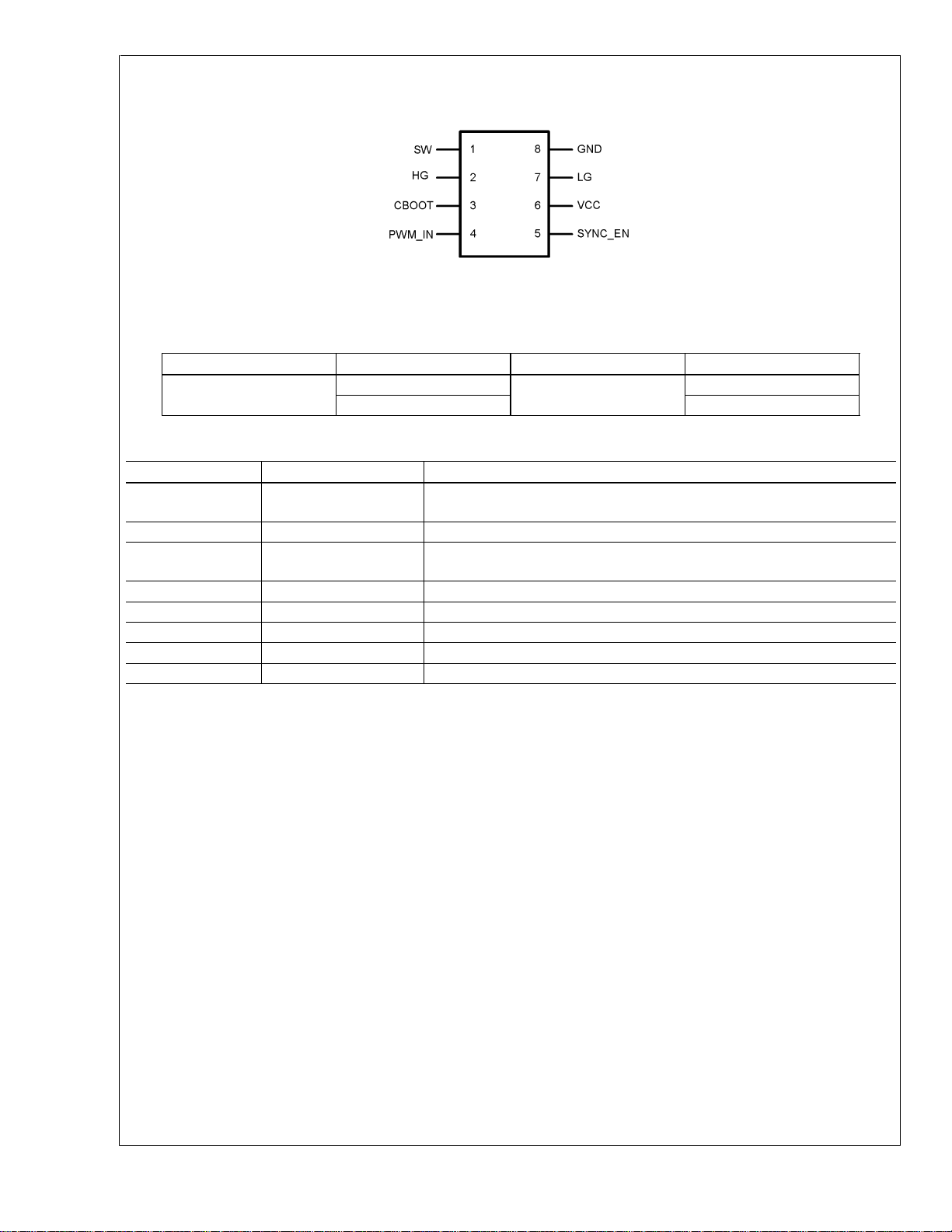
Connection Diagram
LM2722
8-Lead Small Outline Package
Top View
Ordering Information
Order Number Package Type NSC Package Drawing Supplied As
LM2722
LM2722M
LM2722MX 2500 Units/Reel
M08A
Pin Description
Pin Name Function
1SW
2 HG Top gate drive output
3 CBOOT
4 PWM_IN Accepts a 5V-logic control signal
5 SYNC_EN Low gate Enable
6 VCC Connect to +5V supply
7 LG Bottom gate drive output
8 GND Ground
Top driver return. Should be connected to the common node of top
and bottom FETs
Bootstrap. Accepts a bootstrap voltage for powering the high-side
driver
20028902
95 Units/Rail
www.national.com 2
Page 3
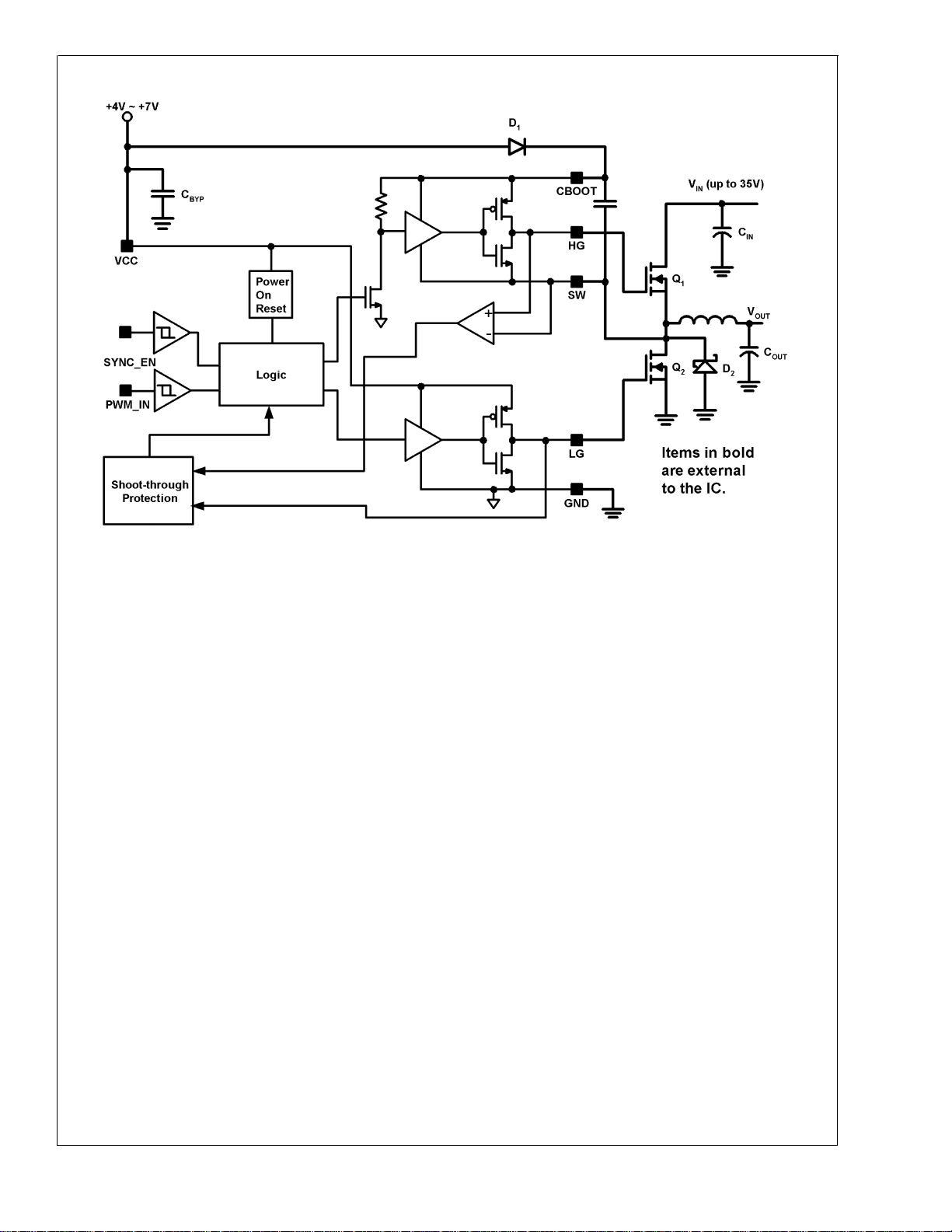
Block Diagram
LM2722
20028904
www.national.com3
Page 4

Absolute Maximum Ratings (Note 1)
If Military/Aerospace specified devices are required,
LM2722
please contact the National Semiconductor Sales Office/
Distributors for availability and specifications.
Storage Temperature −65˚ to 150˚C
ESD Susceptibility
Human Body Model (Note 3) 1kV
Soldering Time, Temperature 10sec., 300˚C
VCC 7.5V
CBOOT 42V
CBOOT to SW 8V
SW to PGND 36V
Junction Temperature +150˚C
Operating Ratings (Note 1)
VCC 4V to 7V
Junction Temperature Range −40˚ to 125˚C
Power Dissipation
(Note 2) 720mW
Electrical Characteristics
VCC = CBOOT = 5V, SW = GND = 0V, unless otherwise specified. Typicals and limits appearing in plain type apply for TA=
T
= +25˚C. Limits appearing in boldface type apply over the entire operating temperature range.
J
Symbol Parameter Condition Min Typ Max Units
POWER SUPPLY
I
q_op
TOP DRIVER
t
4
t
6
t
3
t
5
BOTTOM DRIVER
t
8
t
2
t
7
t
1
LOGIC
V
uvlo_up
V
uvlo_dn
V
uvlo_hys
V
IH_EN
V
IL_EN
Operating Quiescent
Current
Peak Pull-Up Current Test Circuit 1, V
Pull-Up Rds_on I
Peak Pull-down Current Test Circuit 2, V
Pull-down Rds_on I
Rise Time Timing Diagram, C
Fall Time 12 ns
PWM_IN = 0V
= 0.1Ω
CBOOT=IHG
= 0.1Ω
SW=IHG
= 0.7A 0.5 Ω
3.3nF
190 300
= 5V, R
bias
3.0 A
= 0.7A 1.0 Ω
= 5V, R
bias
LOAD
=
−3.2 A
17 ns
Pull-Up Dead Time Timing Diagram 23 ns
Pull-Down Delay Timing Diagram, from
PWM_IN Falling Edge
Peak Pull-Up Current Test Circuit 3, V
bias
= 5V, R
= 0.1Ω
Pull-up Rds_on I
VCC=ILG
Peak Pull-down Current Test Circuit 4, V
= 0.7A 1.0 Ω
= 5V, R
bias
= 0.1Ω
Pull-down Rds_on I
GND=ILG
Rise Time Timing Diagram, C
Fall Time 14 ns
3.3nF
= 0.7A 0.5 Ω
=
LOAD
27 ns
3.2 A
3.2 A
17 ns
Pull-up Dead Time Timing Diagram 28 ns
Pull-down Delay Timing Diagram, from
PWM_IN Rising Edge
Power On Threshold VCC rises from 0V toward
5V
Under-Voltage-Lock-Out
Threshold
Under-Voltage-Lock-Out
Hysteresis
4 3.7 V
13 ns
3.0
2.5
0.7 V
SYNC_EN Pin High Input 2.4 V
SYNC_EN Pin Low Input 0.8 V
µA
V
www.national.com 4
Page 5

Electrical Characteristics (Continued)
VCC = CBOOT = 5V, SW = GND = 0V, unless otherwise specified. Typicals and limits appearing in plain type apply for TA=
T
= +25˚C. Limits appearing in boldface type apply over the entire operating temperature range.
J
Symbol Parameter Condition Min Typ Max Units
I
leak_EN
t
on_min
t
off_min
V
IH_PWM
V
IL_PWM
Note 1: AbsoluteMaximum Ratings are limits beyond which damage to the device may occur. Operating ratings are conditions under which the device operates
correctly. Operating Ratings do not imply guaranteed performance limits.
Note 2: Maximum allowable power dissipation is a function of the maximum junction temperature, T
ambient temperature, T
ambient thermal resistance, θ
Note 3: ESD machine model susceptibility is 100V.
Note 4: If after a rising edge, a falling edge occurs sooner than the specified value, the IC may intermittently fail to turn on the bottom gate when the top gate is
off. As the falling edge occurs sooner and sooner, the driver may start to ignore the pulse and produce no output.
Note 5: If after a falling edge, a rising edge occurs sooner than the specified value, the IC may intermittently fail to turn on the top gate when the bottom gate is
off. As the rising edge occurs sooner and sooner, the driver may start to ignore the pulse and produce no output.
SYNC_EN Pin Leakage
Current
EN=5V −2 2
EN=0V −2 2
Minimum Positive Input
Pulse Width
(Note 4)
Minimum Negative Input
Pulse Width
(Note 5)
PWM_IN High Level Input
Voltage
PWM_IN Low Level Input
Voltage
. The maximum allowable power dissipation at any ambient temperature is calculated using: P
A
, for the LM2722, it is 172˚C/W. For a T
JA
When PWM_IN pin goes
high from 0V
When PWM_IN pin goes
low from 5V
of 150˚C and TAof 25˚C, the maximum allowable power dissipation is 0.7W.
JMAX
2.4
, the junction-to-ambient thermal resistance, θJA, and the
JMAX
MAX
55
55
=(T
0.8
)/θJA. The junction-to-
JMAX-TA
LM2722
µA
ns
V
Timing Diagram
20028903
www.national.com5
Page 6

Test Circuits
LM2722
Test Circuit 1
Test Circuit 3
20028905
20028907
Test Circuit 2
20028906
20028908
Test Circuit 4
www.national.com 6
Page 7

Typical Waveforms
20028913
FIGURE 1. Switching Waveforms of Test Circuit
LM2722
20028915
FIGURE 3. When Input Goes Low
20028914
FIGURE 2. When Input Goes High
Application Information
Minimum Pulse Width
In order for the shoot-through prevention circuitry in the
LM2722 to work properly, the pulses into the PWM_IN pin
must be longer than 55ns. The internal logic waits until the
first FET is off plus 20ns before turning on the opposite FET.
If, after a falling edge, a rising edge occurs sooner than the
specified time, t
the top gate when the bottom gate is off. As the rising edge
occurs sooner and sooner, the driver may start to ignore the
pulse and produce no output. This condition results in the
PWM_IN pin in a high state and neither FET turned on. To
get out of this state, the PWM_IN pin must see a low signal
for greater than 55ns, before the rising edge.
This will also assure that the gate drive bias voltage has
been restored by forcing the top FET source and C
ground first. Then the internal circuitry is reset and normal
operation will resume.
Conversely, if, after a rising edge, a falling edge occurs
sooner than the specified miniumum pulse width, t
, the IC may intermittently fail to turn on
off_min
on_min
boot
, the
20028916
FIGURE 4. Minimum Positive Pulse
IC may intermittently fail to turn on the bottom FET. As the
falling edge occurs sooner and sooner, the driver will start to
ignore the pulse and produce no output. This will result in the
inductor current taking a path through a diode provided
t
off
for non-synchronous operation. The circuit will resume synchronous operation when the rising PWM pulses exceed
55ns in duration.
High Input Voltages or High Output Currents
At input voltages above twice the output voltage and at
higher power levels, the designer may find snubber networks
and gate drive limiting useful in reducing EMI and preventing
injurious transients. A small resistor, 1Ω to 5Ω, between the
driver outputs and the MOSFET gates will slightly increase
to
the rise time and fall time of the output stage and reduce
switching noise. The trade-off is 1% to 2% in efficiency.
A series R-C snubber across in parallel with the bottom FET
can also be used to reduce ringing. Values of 10nF and 10Ω
to 100Ω are a good starting point.
www.national.com7
Page 8

Physical Dimensions inches (millimeters)
unless otherwise noted
8-Lead Small Outline Package
NS Package Number M08A
LM2722 High Speed Synchronous/Asynchronous MOSFET Driver
LIFE SUPPORT POLICY
NATIONAL’S PRODUCTS ARE NOT AUTHORIZED FOR USE AS CRITICAL COMPONENTS IN LIFE SUPPORT
DEVICES OR SYSTEMS WITHOUT THE EXPRESS WRITTEN APPROVAL OF THE PRESIDENT AND GENERAL
COUNSEL OF NATIONAL SEMICONDUCTOR CORPORATION. As used herein:
1. Life support devices or systems are devices or
systems which, (a) are intended for surgical implant
into the body, or (b) support or sustain life, and
whose failure to perform when properly used in
accordance with instructions for use provided in the
labeling, can be reasonably expected to result in a
significant injury to the user.
National Semiconductor
Corporation
Americas
Email: support@nsc.com
www.national.com
National Semiconductor
Europe
Fax: +49 (0) 180-530 85 86
Email: europe.support@nsc.com
Deutsch Tel: +49 (0) 69 9508 6208
English Tel: +44 (0) 870 24 0 2171
Français Tel: +33 (0) 1 41 91 8790
2. A critical component is any component of a life
support device or system whose failure to perform
can be reasonably expected to cause the failure of
the life support device or system, or to affect its
safety or effectiveness.
National Semiconductor
Asia Pacific Customer
Response Group
Tel: 65-2544466
Fax: 65-2504466
Email: ap.support@nsc.com
National Semiconductor
Japan Ltd.
Tel: 81-3-5639-7560
Fax: 81-3-5639-7507
National does not assume any responsibility for use of any circuitry described, no circuit patent licenses are implied and National reserves the right at any time without notice to change said circuitry and specifications.
 Loading...