

Page 1
LM2703
Micropower Step-up DC/DC Converter with 350mA Peak
Current Limit
General Description
The LM2703 is a micropower step-up DC/DC in a small
5-lead SOT-23 package. A current limited, fixed off-time
control scheme conserves operating current resulting in high
efficiency over a wide range of load conditions. The 21V
switch allows for output voltages as high as 20V. The low
400ns off-time permits the use of tiny, low profile inductors
and capacitors to minimize footprint and cost in spaceconscious portable applications. The LM2703 is ideal for
LCD panels requiring low current and high efficiency as well
as white LED applications for cellular phone back-lighting.
The LM2703 can drive up to 4 white LEDs from a single
Li-Ion battery.
Features
n 350mA, 0.7Ω, internal switch
n Uses small surface mount components
n Adjustable output voltage up to 20V
n 2.2V to 7V input range
n Input undervoltage lockout
n 0.01µA shutdown current
n Small 5-Lead SOT-23 package
Applications
n LCD Bias Supplies
n White LED Back-Lighting
n Handheld Devices
n Digital Cameras
n Portable Applications
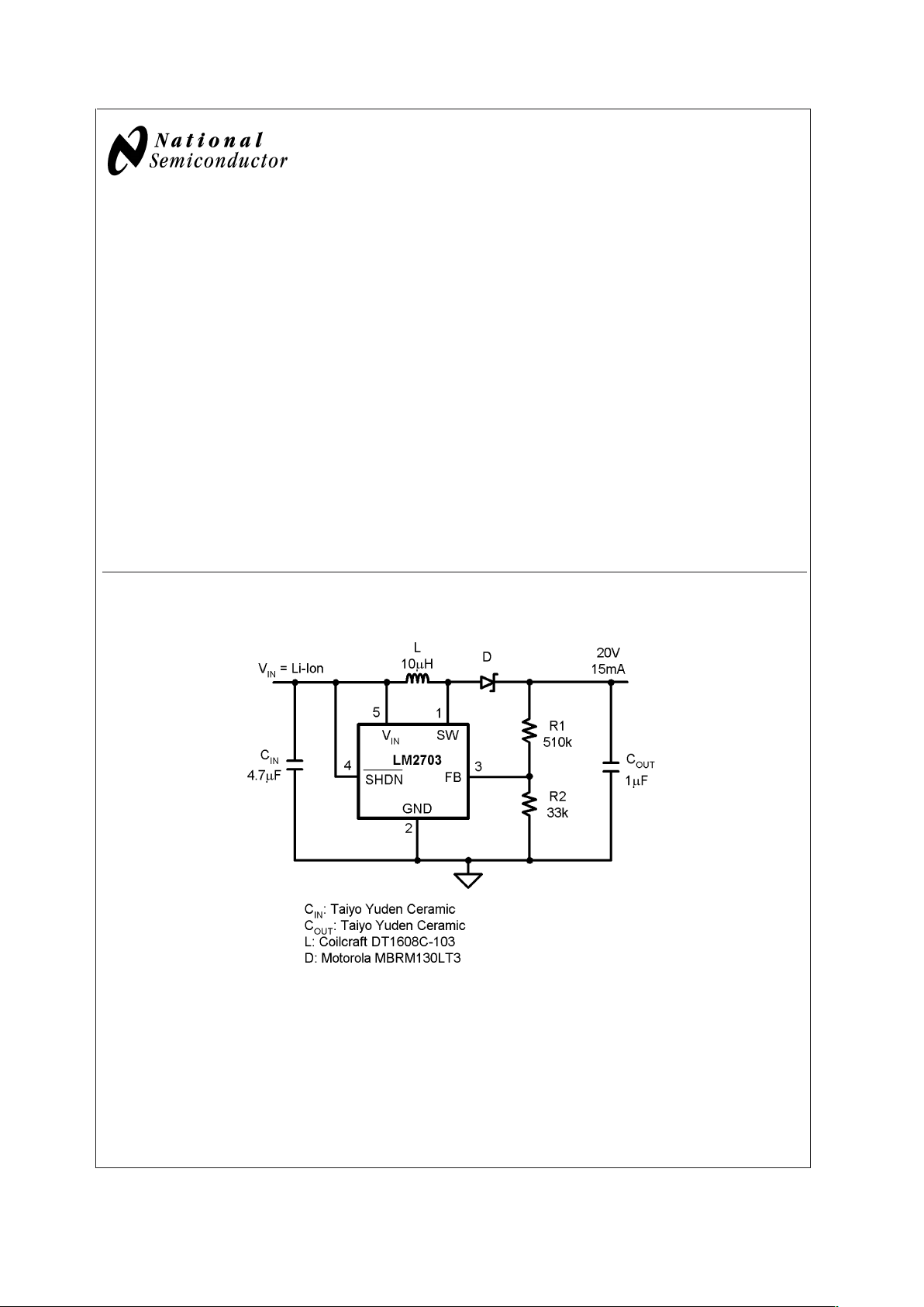
Typical Application Circuit
20030601
FIGURE 1. Typical 20V Application
April 2003
LM2703 Micropower Step-up DC/DC Converter with 350mA Peak Current Limit
© 2003 National Semiconductor Corporation DS200306 www.national.com
Page 2
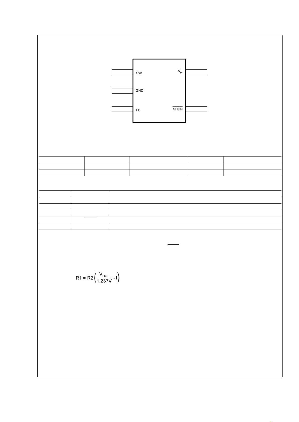
Connection Diagram
Top View
20030602
SOT23-5
T
Jmax
= 125˚C, θJA= 220˚C/W (Note 2)
Ordering Information
Order Number Package Type NSC Package Drawing Top Mark Supplied As
LM2703MF-ADJ SOT23-5 MA05B S48B 1000 Units, Tape and Reel
LM2703MFX-ADJ SOT23-5 MA05B S48B 3000 Units, Tape and Reel
Pin Description/Functions
Pin Name Function
1 SW Power Switch input.
2 GND Ground.
3 FB Output voltage feedback input.
4 SHDN
Shutdown control input, active low.
5V
IN
Analog and Power input.
SW(Pin 1): Switch Pin. This is the drain of the internal
NMOS power switch. Minimize the metal trace area connected to this pin to minimize EMI.
GND(Pin 2): Ground Pin. Tie directly to ground plane.
FB(Pin 3): Feedback Pin. Set the output voltage by selecting
values for R1 and R2 using:
Connect the ground of the feedback network to an AGND
plane which should be tied directly to the GND pin.
SHDN(Pin 4): Shutdown Pin. The shutdown pin is an active
low control. Tie this pin above 1.1V to enable the device. Tie
this pin below 0.3V to turn off the device.
V
IN
(Pin 5): Input Supply Pin. Bypass this pin with a capacitor
as close to the device as possible.
LM2703
www.national.com 2
Page 3

Absolute Maximum Ratings (Note 1)
If Military/Aerospace specified devices are required,
please contact the National Semiconductor Sales Office/
Distributors for availability and specifications.
V
IN
7.5V
SW Voltage 21V
FB Voltage 2V
SHDN Voltage
7.5V
Maximum Junction Temp. T
J
(Note 2)
150˚C
Lead Temperature
(Soldering 10 sec.) 300˚C
Vapor Phase
(60 sec.) 215˚C
Infrared
(15 sec.) 220˚C
ESD Ratings (Note 3)
Human Body Model
Machine Model (Note 4)
2kV
200V
Operating Conditions
Junction Temperature
(Note 5) −40˚C to +125˚C
Supply Voltage 2.2V to 7V
SW Voltage Max. 20.5V
Electrical Characteristics
Specifications in standard type face are for TJ= 25˚C and those in boldface type apply over the full Operating Temperature
Range (T
J
= −40˚C to +125˚C). Unless otherwise specified. VIN=2.2V.
Symbol Parameter Conditions
Min
(Note 5)
Typ
(Note 6)
Max
(Note 5)
Units
I
Q
Device Disabled FB = 1.3V 40 70
µADevice Enabled FB = 1.2V 235 300
Shutdown SHDN = 0V
0.01 2.5
V
FB
FeedbackTrip Point 1.189 1.237 1.269 V
I
CL
Switch Current Limit 275
260
350 400
400
mA
I
B
FB Pin Bias Current FB = 1.23V (Note 7) 30 120 nA
V
IN
Input Voltage Range 2.2 7.0 V
R
DSON
Switch R
DSON
0.7 1.6 Ω
T
OFF
Switch Off Time 400 ns
I
SD
SHDN Pin Current SHDN = VIN,TJ= 25˚C 080
nASHDN = V
IN,TJ
= 125˚C 15
SHDN = GND
0
I
L
Switch Leakage Current VSW= 20V 0.05 5 µA
UVP Input Undervoltage Lockout ON/OFF Threshold 1.8 V
V
FB
Hysteresis
Feedback Hysteresis 8 mV
SHDN
Threshold
SHDN low
0.7 0.3
V
SHDN High
1.1 0.7
θ
JA
Thermal Resistance 220 ˚C/W
Note 1: Absolute maximum ratings are limits beyond which damage to the device may occur. Operating Ratings are conditions for which the device is intended to
be functional, but device parameter specifications may not be guaranteed. For guaranteed specifications and test conditions, see the Electrical Characteristics.
Note 2: The maximum allowable power dissipation is a function of the maximum junction temperature, T
J
(MAX), the junction-to-ambient thermal resistance, θJA,
and the ambient temperature, T
A
. See the Electrical Characteristics table for the thermal resistance. The maximum allowable power dissipation at any ambient
temperature is calculated using: P
D
(MAX) = (T
J(MAX)−TA
)/θJA. Exceeding the maximum allowable power dissipation will cause excessive die temperature.
Note 3: The human body model is a 100 pF capacitor discharged through a 1.5 kΩ resistor into each pin. The machine model is a 200 pF capacitor discharged
directly into each pin.
Note 4: ESD susceptibility using the machine model is 150V for SW pin.
Note 5: All limits guaranteed at room temperature (standard typeface) and at temperature extremes (bold typeface). All room temperature limits are 100%
production tested or guaranteed through statistical analysis. All limits at temperature extremes are guaranteed via correlation using standard Statistical Quality
Control (SQC) methods. All limits are used to calculate Average Outgoing Quality Level (AOQL).
Note 6: Typical numbers are at 25˚C and represent the most likely norm.
Note 7: Feedback current flows into the pin.
LM2703
www.national.com3
Page 4
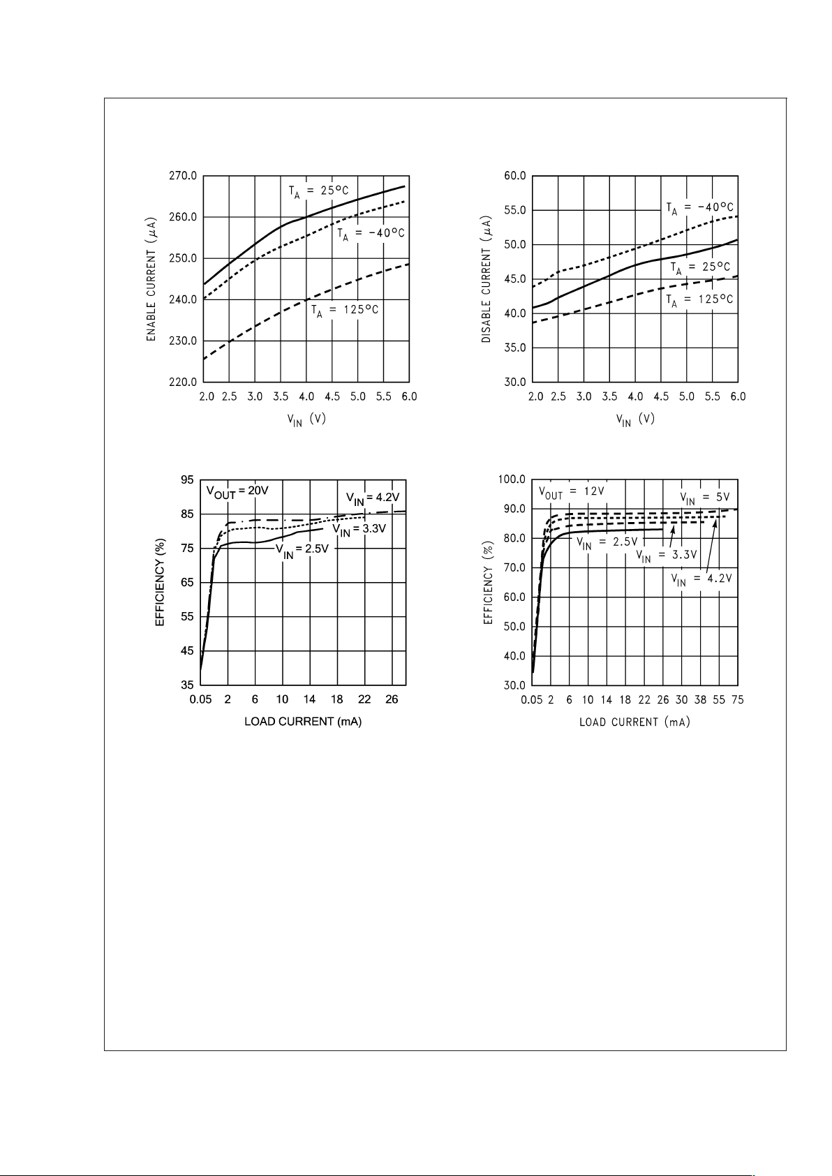
Typical Performance Characteristics
Enable Current vs V
IN
(Part Switching)
Disable Current vs V
IN
(Part Not Switching)
20030605 20030606
Efficiency vs Load Current Efficiency vs Load Current
20030610
20030611
LM2703
www.national.com 4
Page 5

Typical Performance Characteristics (Continued)
Efficiency vs Load Current SHDN Threshold vs V
IN
20030612
20030613
Switch Current Limit vs V
IN
Switch R
DSON
vs V
IN
20030614
20030615
LM2703
www.national.com5
Page 6

Typical Performance Characteristics (Continued)
FB Trip Point and FB Pin Current vs Temperature Output Voltage vs Load Current
20030623
20030622
Step Response Start-Up/Shutdown
20030616
V
OUT
= 20V, VIN= 2.5V
1) Load, 1mA to 10mA to 1mA, DC
2) V
OUT
, 200mV/div, AC
3) I
L
, 200mA/div, DC
T = 50µs/div
20030617
V
OUT
= 20V, VIN= 2.5V
1) SHDN, 1V/div, DC
2) IL, 200mA/div, DC
3) V
OUT
, 20V/div, DC
T = 400µs/div
R
L
= 1.8kΩ
LM2703
www.national.com 6
Page 7

Operation
20030604
FIGURE 2. LM2703 Block Diagram
20030618
V
OUT
= 20V, VIN= 2.5V
1) V
SW
, 20V/div, DC
2) Inductor Current, 200mA/div, DC
3) V
OUT
, 200mV/div, AC
T = 4µs/div
FIGURE 3. Typical Switching Waveform
LM2703
www.national.com7
Page 8

Operation (Continued)
The LM2703 features a constant off-time control scheme.
Operation can be best understood by referring to Figure 2
and Figure 3. Transistors Q1 and Q2 and resistors R3 and
R4 of Figure 2 form a bandgap reference used to control the
output voltage. When the voltage at the FB pin is less than
1.237V, the Enable Comp in Figure 2 enables the device and
the NMOS switch is turned on pulling the SW pin to ground.
When the NMOS switch is on, current begins to flow through
inductor L while the load current is supplied by the output
capacitor C
OUT
. Once the current in the inductor reaches the
current limit, the CL Comp trips and the 400ns One Shot
turns off the NMOS switch.The SW voltage will then rise to
the output voltage plus a diode drop and the inductor current
will begin to decrease as shown in Figure 3. During this time
the energy stored in the inductor is transferred to C
OUT
and
the load. After the 400ns off-time the NMOS switch is turned
on and energy is stored in the inductor again. This energy
transfer from the inductor to the output causes a stepping
effect in the output ripple as shown in Figure 3.
This cycle is continued until the voltage at FB reaches
1.237V. When FB reaches this voltage, the enable comparator then disables the device turning off the NMOS switch and
reducing the Iq of the device to 40uA. The load current is
then supplied solely by C
OUT
indicated by the gradually
decreasing slope at the output as shown in Figure 3. When
the FB pin drops slightly below 1.237V, the enable comparator enables the device and begins the cycle described previously. The SHDN pin can be used to turn off the LM2703
and reduce the Iqto 0.01µA. In shutdown mode the output
voltage will be a diode drop lower than the input voltage.
Application Information
INDUCTOR SELECTION
The appropriate inductor for a given application is calculated
using the following equation:
where VDis the schottky diode voltage, ICLis the switch
current limit found in the Typical Performance Characteris-
tics section, and T
OFF
is the switch off time. When using this
equation be sure to use the minimum input voltage for the
application, such as for battery powered applications. For
the LM2703 constant-off time control scheme, the NMOS
power switch is turned off when the current limit is reached.
There is approximately a 200ns delay from the time the
current limit is reached in the NMOS power switch and when
the internal logic actually turns off the switch. During this
200ns delay, the peak inductor current will increase. This
increase in inductor current demands a larger saturation
current rating for the inductor. This saturation current can be
approximated by the following equation:
Choosing inductors with low ESR decrease power losses
and increase efficiency.
Care should be taken when choosing an inductor. For applications that require an input voltage that approaches the
output voltage, such as when converting a Li-Ion battery
voltage to 5V, the 400ns off time may not be enough time to
discharge the energy in the inductor and transfer the energy
to the output capacitor and load. This can cause a ramping
effect in the inductor current waveform and an increased
ripple on the output voltage. Using a smaller inductor will
cause the I
PK
to increase and will increase the output voltage
ripple further. This can be solved by adding a 4.7pF capacitor across the R
F1
feedback resistor (Figure 2) and slightly
increasing the output capacitor. A smaller inductor can then
be used to ensure proper discharge in the 400ns off time.
DIODE SELECTION
To maintain high efficiency, the average current rating of the
schottky diode should be larger than the peak inductor current, I
PK
. Schottky diodes with a low forward drop and fast
switching speeds are ideal for increasing efficiency in portable applications. Choose a reverse breakdown of the
schottky diode larger than the output voltage.
CAPACITOR SELECTION
Choose low ESR capacitors for the output to minimize output
voltage ripple. Multilayer ceramic capacitors are the best
choice. For most applications, a 1µF ceramic capacitor is
sufficient. For some applications a reduction in output voltage ripple can be achieved by increasing the output capacitor.
Local bypassing for the input is needed on the LM2703.
Multilayer ceramic capacitors are a good choice for this as
well. A 4.7µF capacitor is sufficient for most applications. For
additional bypassing, a 100nF ceramic capacitor can be
used to shunt high frequency ripple on the input.
LAYOUT CONSIDERATIONS
The input bypass capacitor C
IN
, as shown in Figure 1, must
be placed close to the IC. This will reduce copper trace
resistance which effects input voltage ripple of the IC. For
additional input voltage filtering, a 100nF bypass capacitor
can be placed in parallel with C
IN
to shunt any high fre-
quency noise to ground. The output capacitor, C
OUT
, should
also be placed close to the IC. Any copper trace connections
for the Cout capacitor can increase the series resistance,
which directly effects output voltage ripple. The feedback
network, resistors R1 and R2, should be kept close to the FB
pin to minimize copper trace connections that can inject
noise into the system. The ground connection for the feedback resistor network should connect directly to an analog
ground plane. The analog ground plane should tie directly to
the GND pin. If no analog ground plane is available, the
ground connection for the feedback network should tie directly to the GND pin. Trace connections made to the inductor and schottky diode should be minimized to reduce power
dissipation and increase overall efficiency.
LM2703
www.national.com 8
Page 9

Application Information (Continued)
20030609
FIGURE 4. White LED Application
20030619
FIGURE 5. Li-Ion 5V Application
20030620
FIGURE 6. Li-Ion 12V Application
LM2703
www.national.com9
Page 10

Application Information (Continued)
20030621
FIGURE 7. 5V to 12V Application
LM2703
www.national.com 10
Page 11

Physical Dimensions inches (millimeters) unless otherwise noted
5-Lead Small Outline Package (M5)
For Ordering, Refer to Ordering Information Table
NS Package Number MA05B
LIFE SUPPORT POLICY
NATIONAL’S PRODUCTS ARE NOT AUTHORIZED FOR USE AS CRITICAL COMPONENTS IN LIFE SUPPORT
DEVICES OR SYSTEMS WITHOUT THE EXPRESS WRITTEN APPROVAL OF THE PRESIDENT AND GENERAL
COUNSEL OF NATIONAL SEMICONDUCTOR CORPORATION. As used herein:
1. Life support devices or systems are devices or
systems which, (a) are intended for surgical implant
into the body, or (b) support or sustain life, and
whose failure to perform when properly used in
accordance with instructions for use provided in the
labeling, can be reasonably expected to result in a
significant injury to the user.
2. A critical component is any component of a life
support device or system whose failure to perform
can be reasonably expected to cause the failure of
the life support device or system, or to affect its
safety or effectiveness.
National Semiconductor
Americas Customer
Support Center
Email: new.feedback@nsc.com
Tel: 1-800-272-9959
National Semiconductor
Europe Customer Support Center
Fax: +49 (0) 180-530 85 86
Email: europe.support@nsc.com
Deutsch Tel: +49 (0) 69 9508 6208
English Tel: +44 (0) 870 24 0 2171
Français Tel: +33 (0) 1 41 91 8790
National Semiconductor
Asia Pacific Customer
Support Center
Fax: +65-6250 4466
Email: ap.support@nsc.com
Tel: +65-6254 4466
National Semiconductor
Japan Customer Support Center
Fax: 81-3-5639-7507
Email: jpn.feedback@nsc.com
Tel: 81-3-5639-7560
www.national.com
LM2703 Micropower Step-up DC/DC Converter with 350mA Peak Current Limit
National does not assume any responsibility for use of any circuitry described, no circuit patent licenses are implied and National reserves the right at any time without notice to change said circuitry and specifications.
 Loading...