

Page 1

LM2682
Switched Capacitor Voltage Doubling Inverter
LM2682 Switched Capacitor Voltage Doubling Inverter
November 1999
General Description
The LM2682 is a CMOS charge-pump voltage inverter capable of converting positive voltage in the range of +2.0V to
+5.5V to the corresponding doubled negative voltage of
−4.0V to −11.0V respectively. The LM2682 uses three low
cost capacitors to provide 10 mA of output current without
the cost, size, and EMI related to inductor based circuits.
With an operating current of only 150µAandanoperatingefficiency greater than 90%with most loads, the LM2682 provides ideal performance for battery powered systems. The
LM2682 offers a switching frequency of 6 kHz.
Features
n Inverts then doubles input supply voltage
n Small MSOP-8 package (mini SO-8) and SO-8 package
n 90Ω typical output impedance
n 94%typical power efficiency at 10 mA
Applications
n LCD contrast biasing
n GaAs power amplifier biasing
n Interface power supplies
n Handheld instrumentation
n Laptop computers and PDAs
Typical Operating Circuit and Pin Configuration
8-Pin MSOP
or 8-Pin SOIC
DS100997-2
DS100997-1
Ordering Information
Order Number Package Package Number Package Marking Supplied As
LM2682MM MSOP-8 MUA08A S11A Tape and Reel (1000 units/reel)
LM2682MMX MSOP-8 MUA08A S11A Tape and Reel (3500 units/reel)
LM2682M SO-8 M08A LM2682M Rail (95 units/rail)
LM2682MX SO-8 M08A LM2682M Tape and Reel (2500 units/reel)
© 1999 National Semiconductor Corporation DS100997 www.national.com
Page 2

Absolute Maximum Ratings (Note 1)
If Military/Aerospace specified devices are required,
LM2682
please contact the National SemiconductorSales Office/
Distributors for availability and specifications.
Input Voltage (V
V
dV/dT 1V/µsec
IN
V
OUT
V
Short-Circuit Duration Continuous
OUT
Storage Temperature −65˚C to +150˚C
Lead Temperature Soldering +300˚C
) +5.8V
IN
−11.6V
MSOP-8 300 mW
SO-8 470 mW
T
JMAX
Operating Ratings
ESD Susceptibility (Note 3)
Human Body Model
Machine Model
Ambient Temp. Range −40˚C to +85˚C
Junction Temp. Range −40˚C to +125˚C
Power Dissipation (Note 2)
LM2682
Electrical Characteristics
typeface apply over the full operating ambient temperature range, −40˚C to +85˚C, limits with standard typeface apply for T
=
25˚C.
V
IN
=
5V and C
=
=
=
C
C
1
3.3µF unless otherwise specified. Limits with bold
2
3
+150˚C
2kV
200V
A
Symbol Parameter Conditions Min Typical
Max Units
(Note 4)
V
IN
I
IN
R
OUT
Supply Voltage Range R
Supply Current Open Circuit, No Load 150 300
V
Source Resistance I
OUT
=
2kΩ 2.0 5.5 V
L
400
=
10 mA 90 150 Ω
L
µA
200
=
I
5 mA, V
f
OSC
f
SW
η
POWER
η
VOLTAGE
Note 1: Absolute Maximum Ratings are thosevalues beyond which damage to the device may occur. Operating Ratings indicate conditions for whichthe device is
intended to be functional, but do not guarantee specific performance limits. For guaranteed specifications and test conditions, see the Electrical Characteristics.
Note 2: The maximum power dissipationmustbede-rated at elevated temperatures (only needed for T
ture), θ
maximum power dissipation at any temperature is:
PDiss
Note 3: The human body model is a 100 pF capacitor discharged through a 1.5 kΩ resistor into each pin.The machine model is a 200pF capacitor discharged di-
rectly into each pin.
Note 4: Typical numbers are at 25˚C and represent the most likely norm.
Note 5: The output switches operate at one half of the oscillator frequency, f
Note 6: The minimum specification is guaranteed by design and is not tested.
Oscillator Frequency (Note 5) 12 30 kHz
Switching Frequency (Note 5) 6 15 kHz
Power Efficiency R
Voltage Conversion Efficiency 99.9
(junction to ambient thermal resistance) and TA(ambient temperature). θ
J-A
MAX
=
(T
JMAX−TA
)/θ
up to the value listed in the Absolute Maximum Ratings.
J-A
L
=
L
=
2 V 110 250 Ω
IN
2k (Note 6) 90 93
>
85˚C) and is limited by T
is 140˚C/W for the SO-8 package and 220˚C/W for the MSOP-8 package. The
J-A
=
.
2f
OSC
SW
A
JMAX
%
%
(maximum junction tempera-
Pin Description
Pin Number Symbol Description
1C
2C
3C
4V
5 GND Device ground
6V
7C
8 NC No Connection
− Capacitor C1negative terminal
1
+ Capacitor C2positive terminal
2
− Capacitor C2negative terminal
2
Negative output voltage (−2VIN)
OUT
Power supply voltage
IN
+ Capacitor C1positive terminal
1
www.national.com 2
Page 3
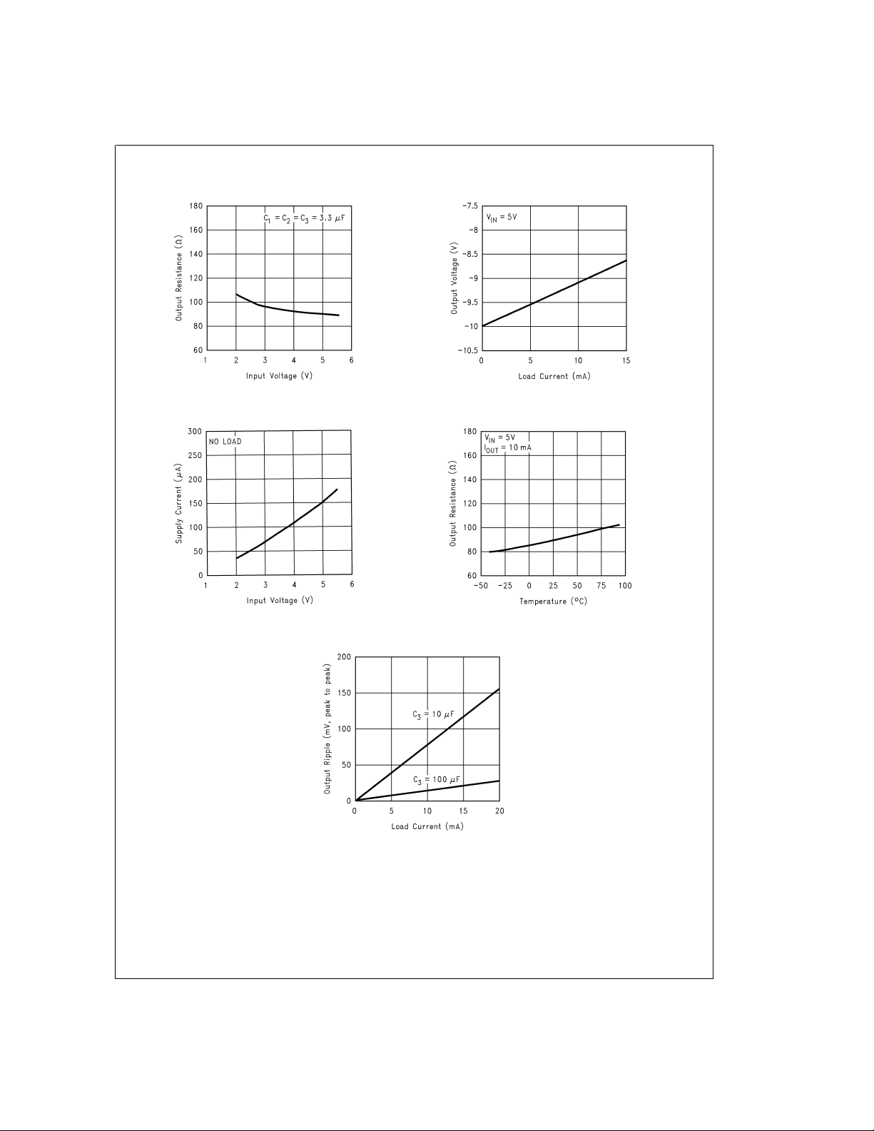
Typical Performance Charactistics V
Output Resistance vs Input Voltage
IN
=
5V and T
=
25˚C unless otherwise noted.
A
Output Voltage vs Load Current
LM2682
Supply Current vs Input Voltage
Output Voltage Ripple vs Load Current
DS100997-6
DS100997-8
DS100997-7
Output Resistance vs Temperature
DS100997-9
DS100997-10
www.national.com3
Page 4

Basic Application Circuits
LM2682
DS100997-3
FIGURE 1. Doubling Voltage Inverter
FIGURE 2. +5V to −5V Regulated Voltage Converter
Application Information
Voltage Doubling Inverter
The main application of the LM2682 is to generate a negative voltage that is twice the positive input voltage. This circuit requires onlythree external capacitorsand is connected
as shown in
efficiency of the circuit is determined by the output resistance. A derivation of the output resistance is shown below:
R
OUT
Using the assumption that all four switches have the same
ON resistance our equation becomes:
R
OUT
www.national.com 4
=
=
Figure 1
. It is important to keep in mind that the
2(R
SW1+RSW2
2(R
SW1+RSW2
1/(f
OSC
16R
1/(f
OSC
SW
+ESRC1+R
+ESRC1+R
xC1) + 1/(f
xC2) + ESR
OSC
SW3+RSW4
SW3+RSW4
+ 4ESRC1+ 4ESRC2+ ESRC3+
xC1) + 1/(f
OSC
xC2)
+ESRC2)+
+ESRC2)+
C3
DS100997-4
Output resistance is typically 90Ω with an input voltage of
+5V, an operating temperature of 25˚C, and using low ESR
3.3 µF capacitors. This equation shows the importance of
capacitor selection. Large value, low ESR capacitors will reduce the output resistancesignificantly but willalso requirea
larger overall circuit. Smaller capacitors will take up less
space but can lower efficiency greatly if the ESR is large.
Also to be considered is that C1 must be rated at 6 VDC or
greater while C2 andC3 mustbe ratedat 12VDC orgreater.
The amount of output voltage ripple isdetermined by theoutput capacitor C3 and the output current as shown in this
equation:
V
RIPPLE P-P
=
x (2xESRC3+ 1/[2x(f
I
OUT
OSC
xC3)])
Once again a largercapacitor with smaller ESRwill give better results.
Page 5

Application Information (Continued)
+5V to −5V Regulated Voltage Converter
Another application in which the LM2682 can be used is for
generating a −5V regulated supply from a +5V unregulated
supply. This involves using an op-amp and a reference and
is connected as shown in
chosen for its low cost and versatility and the LM4040-5.0
reference was chosen for its low bias current requirement.
Of course othercombinations may be used atthe designer’s
discretion to fit accuracy, efficiency, and cost requirements.
With this configuration the circuit is well regulated and isstill
capable of providing nearly10 mAof output current.With a9
mA load the circuit can typically maintain 5%regulation on
the output voltage withthe input varyinganywhere from4.5V
to the maximum of 5.5V. With less load the results are even
better.Voltage ripple concerns are reducedin this case since
the ripple at the output of the LM2682 is reduced at the output by the PSRR of the op-amp used.
Figure 2
. The LM358 op-amp was
Paralleling Devices
Any number of devices can be paralleled to reduce the output resistance. As shown in
its own pumping capacitors, C1 and C2,but only one shared
output capacitor is required. The effective output resistance
is the output resistance of onedevice divided bythe number
of devices used inparallel. Parallelingdevices also gives the
capability of increasing the maximum output current. The
maximum output current now becomes the maximum output
current for one device multiplied by the number of devices
used in parallel.For example, if you parallel two devices you
can get 20 mA of output current and have half the output resistance of one device supplying 10 mA.
Figure 3
, each device musthave
LM2682
FIGURE 3. Paralleling Devices
DS100997-5
www.national.com5
Page 6

Physical Dimensions inches (millimeters) unless otherwise noted
LM2682
8 Lead (0.150” Wide) Molded Small Outline Package, JEDEC
NS Package Number M08A
www.national.com 6
Page 7

Physical Dimensions inches (millimeters) unless otherwise noted (Continued)
LM2682 Switched Capacitor Voltage Doubling Inverter
Surface Mount Mini SO-8 Package
NS Package Number MUA08A
LIFE SUPPORT POLICY
NATIONAL’S PRODUCTS ARE NOT AUTHORIZED FOR USE AS CRITICAL COMPONENTS IN LIFE SUPPORT
DEVICES OR SYSTEMS WITHOUT THE EXPRESS WRITTEN APPROVAL OF THE PRESIDENT AND GENERAL
COUNSEL OF NATIONAL SEMICONDUCTOR CORPORATION. As used herein:
1. Life support devices or systems are devices or
systems which, (a) are intended for surgical implant
into the body, or (b) support or sustain life, and
whose failure to perform when properly used in
accordance with instructions for use provided in the
2. A critical component is any component of a life
support device or system whose failure to perform
can be reasonably expected to cause the failure of
the life support device or system, or to affect its
safety or effectiveness.
labeling, can be reasonably expected to result in a
significant injury to the user.
National Semiconductor
Corporation
Americas
Tel: 1-800-272-9959
Fax: 1-800-737-7018
Email: support@nsc.com
www.national.com
National does not assume any responsibility for use of any circuitry described, no circuit patent licenses are implied and National reserves the right at any time without notice to change said circuitry and specifications.
National Semiconductor
Europe
Fax: +49 (0) 1 80-530 85 86
Email: europe.support@nsc.com
Deutsch Tel: +49 (0) 1 80-530 85 85
English Tel: +49 (0) 1 80-532 78 32
Français Tel: +49 (0) 1 80-532 93 58
Italiano Tel: +49 (0) 1 80-534 16 80
National Semiconductor
Asia Pacific Customer
Response Group
Tel: 65-2544466
Fax: 65-2504466
Email: sea.support@nsc.com
National Semiconductor
Japan Ltd.
Tel: 81-3-5639-7560
Fax: 81-3-5639-7507
 Loading...