

Page 1
LM2679
SIMPLE SWITCHER
®
5A Step-Down Voltage Regulator
with Adjustable Current Limit
LM2679 SIMPLE SWITCHER 5A Step-Down Voltage Regulator with Adjustable Current Limit
April 2005
General Description
The LM2679 series of regulators are monolithic integrated
circuits which provide all of the active functions for a stepdown (buck) switching regulator capable of driving up to 5A
loads with excellent line and load regulation characteristics.
High efficiency (
ON-resistance DMOS power switch. The series consists of
fixed output voltages of 3.3V, 5V and 12V and an adjustable
output version.
The SIMPLE SWITCHER concept provides for a complete
design using a minimum number of external components. A
high fixed frequency oscillator (260KHz) allows the use of
physically smaller sized components. A family of standard
inductors for use with the LM2679 are available from several
manufacturers to greatly simplify the design process.
Other features include the ability to reduce the input surge
current at power-ON by adding a softstart timing capacitor to
gradually turn on the regulator. The LM2679 series also has
built in thermal shutdown and resistor programmable current
limit of the power MOSFET switch to protect the device and
load circuitry under fault conditions. The output voltage is
guaranteed to a
controlled to within a
>
90%) is obtained through the use of a low
±
2% tolerance. The clock frequency is
±
11% tolerance.
Typical Application
Features
n Efficiency up to 92%
n Simple and easy to design with (using off-the-shelf
external components)
n Resistor programmable peak current limit over a range
of 3A to 7A.
n 120 mΩ DMOS output switch
n 3.3V, 5V and 12V fixed output and adjustable (1.2V to
37V ) versions
±
n
2%maximum output tolerance over full line and load
conditions
n Wide input voltage range: 8V to 40V
n 260 KHz fixed frequency internal oscillator
n Softstart capability
n −40 to +125˚C operating junction temperature range
Applications
n Simple to design, high efficiency (>90%) step-down
switching regulators
n Efficient system pre-regulator for linear voltage
regulators
n Battery chargers
10084703
SIMPLE SWITCHER®is a registered trademark of National Semiconductor Corporation.
© 2005 National Semiconductor Corporation DS100847 www.national.com
Page 2
Connection Diagrams and Ordering Information
LM2679
TO-263 Package
Top View
TO-220 Package
Top View
Order Number
LM2679S-3.3, LM2679S-5.0,
LM2679S-12 or LM2679S-ADJ
See NSC Package Number TS7B
See NS package Number SRC14A
10084701
Order Number
10084702
LM2679T-3.3, LM2679T-5.0,
LM2679T-12 or LM2679T-ADJ
See NSC Package Number TA07B
Top View
10084735
LLP-14
Ordering Information for LLP Package
Output Voltage Order Information Package Marking Supplied As
12 LM2679SD-12 S0003FB 250 Units on Tape and Reel
12 LM2679SDX-12 S0003FB 2500 Units on Tape and Reel
3.3 LM2679SD-3.3 S0003HB 250 Units on Tape and Reel
3.3 LM2679SDX-3.3 S0003HB 2500 Units on Tape and Reel
5.0 LM2679SD-5.0 S0003JB 250 Units on Tape and Reel
5.0 LM2679SDX-5.0 S0003JB 2500 Units on Tape and Reel
ADJ LM2679SD-ADJ S0003KB 250 Units on Tape and Reel
ADJ LM2679SDX-ADJ S0003KB 2500 Units on Tape and Reel
www.national.com 2
Page 3
LM2679
Absolute Maximum Ratings (Note 1)
If Military/Aerospace specified devices are required,
please contact the National Semiconductor Sales Office/
Distributors for availability and specifications.
Input Supply Voltage 45V
Storage Temperature Range −65˚C to 150˚C
Soldering Temperature
Wave 4 sec, 260˚C
Infrared 10 sec, 240˚C
Vapor Phase 75 sec, 219˚C
Softstart Pin Voltage −0.1V to 6V
Switch Voltage to Ground −1V to V
IN
Operating Ratings
Boost Pin Voltage VSW+8V
Feedback Pin Voltage −0.3V to 14V
Power Dissipation Internally Limited
Supply Voltage 8V to 40V
Junction Temperature Range (T
) −40˚C to 125˚C
J
ESD (Note 2) 2 kV
Electrical Characteristics Limits appearing in bold type face apply over the entire junction temperature
range of operation, −40˚C to 125˚C. Specifications appearing in normal type apply for T
A=TJ
= 25˚C. R
ADJ
= 5.6KΩ
LM2679-3.3
Symbol Parameter Conditions Typical Min Max Units
(Note 3) (Note 4) (Note 4)
V
OUT
η Efficiency V
Output Voltage VIN= 8V to 40V, 100mA ≤ I
= 12V, I
IN
=5A 82 %
LOAD
≤ 5A 3.3 3.234/3.201 3.366/3.399 V
OUT
LM2679-5.0
Symbol Parameter Conditions Typical Min Max Units
(Note 3) (Note 4) (Note 4)
V
OUT
η Efficiency V
Output Voltage VIN= 8V to 40V, 100mA ≤ I
= 12V, I
IN
=5A 84 %
LOAD
≤ 5A 5.0 4.900/4.850 5.100/5.150 V
OUT
LM2679-12
Symbol Parameter Conditions Typical Min Max Units
(Note 3) (Note 4) (Note 4)
V
OUT
η Efficiency V
Output Voltage VIN= 15V to 40V, 100mA ≤ I
= 24V, I
IN
=5A 92 %
LOAD
≤ 5A 12 11.76/11.64 12.24/12.36 V
OUT
LM2679-ADJ
Symbol Parameter Conditions Typ Min Max Units
(Note 3) (Note 4) (Note 4)
V
FB
η Efficiency V
Feedback
Voltage
VIN= 8V to 40V, 100mA ≤ I
Programmed for 5V
V
OUT
= 12V, I
IN
=5A 84 %
LOAD
OUT
≤ 5A
1.21 1.186/1.174 1.234/1.246 V
www.national.com3
Page 4
All Output Voltage Versions Electrical Characteristics
LM2679
Limits appearing in bold type face apply over the entire junction temperature range of operation, −40˚C to 125˚C. Specifications appearing in normal type apply for T
versions and V
=24V for the 12V version.
IN
Symbol Parameter Conditions Typ Min Max Units
DEVICE PARAMETERS
I
Q
Quiescent
V
FEEDBACK
= 8V 4.2 6 mA
Current
For 3.3V, 5.0V, and ADJ Versions
V
FEEDBACK
= 15V
For 12V Versions
V
ADJ
Current Limit
Adjust Voltage
I
CL
I
L
R
DS(ON)
Current Limit R
Output Leakage
Current
Switch
= 5.6KΩ, (Note 5) 6.3 5.5/5.3 7.6/8.1 A
ADJ
VIN= 40V, Softstart Pin = 0V
V
V
I
SWITCH
=0V
SWITCH
= −1V
SWITCH
= 5A 0.12 0.14/0.225 Ω
On-Resistance
f
O
Oscillator
Measured at Switch Pin 260 225 280 kHz
Frequency
D Duty Cycle Maximum Duty Cycle 91 %
Minimum Duty Cycle 0 %
I
V
BIAS
SFST
Feedback Bias
Current
Softstart
V
FEEDBACK
= 1.3V
ADJ Version Only
Threshold
Voltage
I
SFST
Softstart Pin
Softstart Pin = 0V
Current
θ
JA
θ
JA
Thermal
Resistance
T Package, Junction to Ambient 65
(Note 6)
T Package, Junction to Ambient 45
(Note 7)
θ
JC
θ
JA
T Package, Junction to Case 2
S Package, Junction to Ambient 56 ˚C/W
(Note 8)
θ
JA
S Package, Junction to Ambient 35
(Note 9)
θ
JA
S Package, Junction to Ambient 26
(Note 10)
θ
JC
θ
JA
S Package, Junction to Case 2 ++
SD Package, Junction to Ambient 55
(Note 11)
θ
JA
SD Package, Junction to Ambient 29
(Note 12)
= 25˚C. Unless otherwise specified VIN=12V for the 3.3V, 5V and Adjustable
A=TJ
1.21 1.181/1.169 1.229/1.246 V
1.0
6
85 nA
0.63 0.53 0.74 V
3.7 6.9 µA
1.5
15
mA
mA
˚C/W
www.national.com 4
Page 5

All Output Voltage Versions
Electrical Characteristics
Note 1: Absolute Maximum Ratings are limits beyond which damage to the device may occur. Operating Ratings indicate conditions under which of the device is
guaranteed. Operating Ratings do not imply guaranteed performance limits. For guaranteed performance limits and associated test condition, see the electrical
Characteristics tables.
Note 2: ESD was applied using the human-body model, a 100pF capacitor discharged through a 1.5 kΩ resistor into each pin.
Note 3: Typical values are determined with T
Note 4: All limits are guaranteed at room temperature (standard type face) and at temperature extremes (bold type face). All room temperature limits are 100%
tested during production with T
methods. All limits are used to calculate Average Outgoing Quality Level (AOQL).
Note 5: The peak switch current limit is determined by the following relationship: I
Note 6: Junction to ambient thermal resistance (no external heat sink) for the 7 lead TO-220 package mounted vertically, with
board with minimum copper area.
Note 7: Junction to ambient thermal resistance (no external heat sink) for the 7 lead TO-220 package mounted vertically, with
containing approximately 4 square inches of (1 oz.) copper area surrounding the leads.
Note 8: Junction to ambient thermal resistance for the 7 lead TO-263 mounted horizontally against a PC board area of 0.136 square inches (the same size as the
TO-263 package) of 1 oz. (0.0014 in. thick) copper.
Note 9: Junction to ambient thermal resistance for the 7 lead TO-263 mounted horizontally against a PC board area of 0.4896 square inches (3.6 times the area
of the TO-263 package) of 1 oz. (0.0014 in. thick) copper.
Note 10: Junction to ambient thermal resistance for the 7 lead TO-263 mounted horizontally against a PC board copper area of 1.0064 square inches (7.4 times
the area of the TO-263 package) of 1 oz. (0.0014 in. thick) copper. Additional copper area will reduce thermal resistance further. See the thermal model in Switchers
Made Simple
Note 11: Junction to ambient thermal resistance for the 14-lead LLP mounted on a PC board copper area equal to the die attach paddle.
Note 12: Junction to ambient thermal resistance for the 14-lead LLP mounted on a PC board copper area using 12 vias to a second layer of copper equal to die
attach paddle. Additional copper area will reduce thermal resistance further. For layout recommendations, refer to Application Note AN-1187.
®
software.
A=TJ
A=TJ
= 25˚C. All limits at temperature extremes are guaranteed via correlation using standard standard Quality Control (SQC)
(Continued)
= 25˚C and represent the most likely norm.
=37,125/ R
CL
ADJ
.
1
⁄2inch leads in a socket, or on a PC
1
⁄2inch leads soldered to a PC board
LM2679
www.national.com5
Page 6

Typical Performance Characteristics
LM2679
Normalized
Output Voltage Line Regulation
10084704
Efficiency vs Input Voltage Efficiency vs I
10084706 10084707
LOAD
Switch Current Limit Operating Quiescent Current
10084705
10084708 10084709
www.national.com 6
Page 7
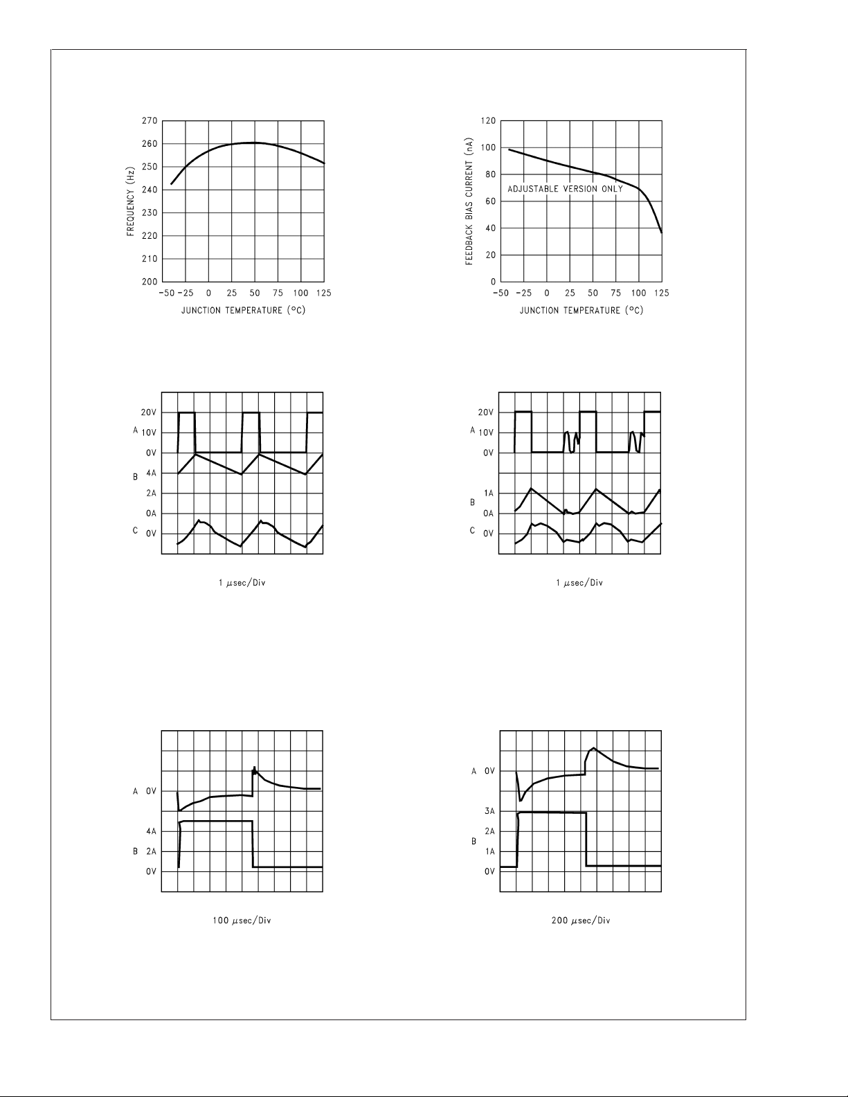
Typical Performance Characteristics (Continued)
Switching Frequency Feedback Pin Bias Current
LM2679
Continuous Mode Switching Waveforms
= 20V, V
V
L=10µH,C
A: VSWPin Voltage, 10 V/div.
B: Inductor Current, 2 A/div
C: Output Ripple Voltage, 20 mV/div AC-Coupled
IN
OUT
= 5V, I
OUT
= 400 µF, C
=5A
LOAD
ESR=13mΩ
OUT
10084715
Horizontal Time Base: 1 µs/div
Load Transient Response for Continuous Mode
L=10µH,C
= 20V, V
V
IN
= 400 µF, C
OUT
OUT
OUT
=5V
ESR=13mΩ
10084712
10084713
Discontinuous Mode Switching Waveforms
V
= 20V, V
IN
L=10µH,C
A: VSWPin Voltage, 10 V/div.
B: Inductor Current, 1 A/div
C: Output Ripple Voltage, 20 mV/div AC-Coupled
OUT
= 400 µF, C
OUT
= 5V, I
= 500 mA
LOAD
ESR=13mΩ
OUT
10084716
Horizontal Time Base: 1 µs//iv
Load Transient Response for Discontinuous Mode
V
L=10µH,C
= 20V, V
IN
= 400 µF, C
OUT
OUT
= 5V,
ESR=13mΩ
OUT
A: Output Voltage, 100 mV//div, AC-Coupled.
B: Load Current: 500 mA to 5A Load Pulse
Horizontal Time Base: 100 µs/div
10084717
A: Output Voltage, 100 mV/div, AC-Coupled.
10084718
B: Load Current: 200 mA to 3A Load Pulse
Horizontal Time Base: 200 µs/div
www.national.com7
Page 8
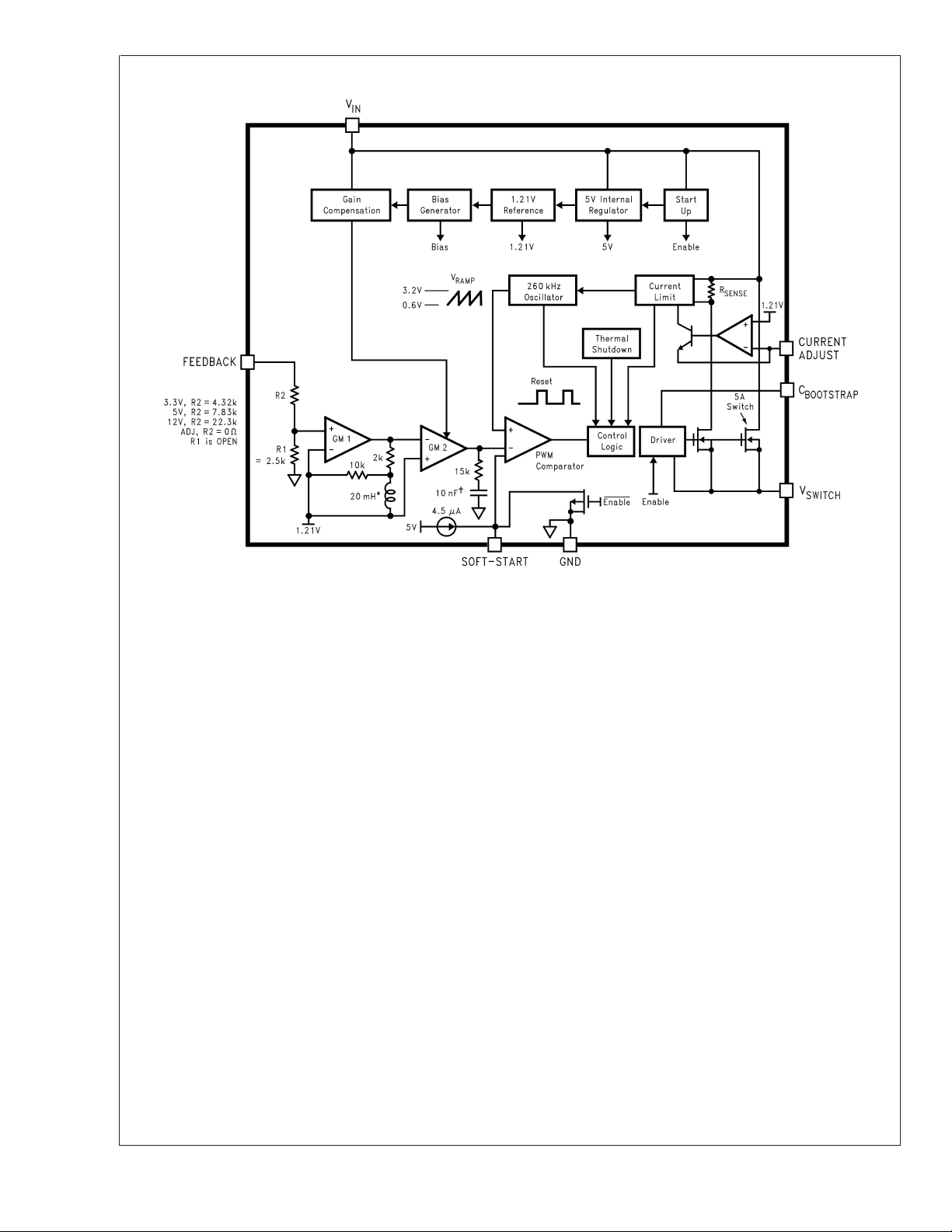
Block Diagram
LM2679
* Active Inductor Patent Number 5,514,947
†
Active Capacitor Patent Number 5,382,918
10084714
www.national.com 8
Page 9

Application Hints
The LM2679 provides all of the active functions required for
a step-down (buck) switching regulator. The internal power
switch is a DMOS power MOSFET to provide power supply
designs with high current capability, up to 5A, and highly
efficient operation.
The LM2679 is part of the SIMPLE SWITCHER family of
power converters. A complete design uses a minimum number of external components, which have been predetermined from a variety of manufacturers. Using either this
data sheet or a design software program called LM267X
Made Simple (version 2.0) a complete switching power
supply can be designed quickly. The software is provided
free of charge and can be downloaded from National Semiconductor’s Internet site located at http://www.national.com.
SWITCH OUTPUT
This is the output of a power MOSFET switch connected
directly to the input voltage. The switch provides energy to
an inductor, an output capacitor and the load circuitry under
control of an internal pulse-width-modulator (PWM). The
PWM controller is internally clocked by a fixed 260KHz
oscillator. In a standard step-down application the duty cycle
(Time ON/Time OFF) of the power switch is proportional to
the ratio of the power supply output voltage to the input
voltage. The voltage on pin 1 switches between Vin (switch
ON) and below ground by the voltage drop of the external
Schottky diode (switch OFF).
INPUT
The input voltage for the power supply is connected to pin 2.
In addition to providing energy to the load the input voltage
also provides bias for the internal circuitry of the LM2679.
For guaranteed performance the input voltage must be in the
range of 8V to 40V. For best performance of the power
supply the input pin should always be bypassed with an input
capacitor located close to pin 2.
C BOOST
A capacitor must be connected from pin 3 to the switch
output, pin 1. This capacitor boosts the gate drive to the
internal MOSFET above Vin to fully turn it ON. This minimizes conduction losses in the power switch to maintain high
efficiency. The recommended value for C Boost is 0.01µF.
CURRENT ADJUST
A key feature of the LM2679 is the ability to tailor the peak
switch current limit to a level required by a particular application. This alleviates the need to use external components
that must be physically sized to accommodate current levels
(under shorted output conditions for example) that may be
much higher than the normal circuit operating current requirements.
A resistor connected from pin 5 to ground establishes a
current (I
(pin 5)
=1.2V/R
) that sets the peak current
ADJ
through the power switch. The maximum switch current is
fixed at a level of 37,125 / R
ADJ
.
FEEDBACK
This is the input to a two-stage high gain amplifier, which
drives the PWM controller. It is necessary to connect pin 6 to
the actual output of the power supply to set the dc output
voltage. For the fixed output devices (3.3V, 5V and 12V
outputs), a direct wire connection to the output is all that is
required as internal gain setting resistors are provided inside
the LM2679. For the adjustable output version two external
resistors are required to set the dc output voltage. For stable
operation of the power supply it is important to prevent
coupling of any inductor flux to the feedback input.
SOFTSTART
A capacitor connected from pin 7 to ground allows for a slow
turn-on of the switching regulator. The capacitor sets a time
delay to gradually increase the duty cycle of the internal
power switch. This can significantly reduce the amount of
surge current required from the input supply during an abrupt
application of the input voltage. If softstart is not required this
pin should be left open circuited.
DAP (LLP PACKAGE)
The Die Attach Pad (DAP) can and should be connected to
PCB Ground plane/island. For CAD and assembly guidelines refer to Application Note AN-1187 at http://
power.national.com.
LM2679
GROUND
This is the ground reference connection for all components
in the power supply. In fast-switching, high-current applications such as those implemented with the LM2679, it is
recommended that a broad ground plane be used to minimize signal coupling throughout the circuit
www.national.com9
Page 10

Application Hints (Continued)
DESIGN CONSIDERATIONS
LM2679
10084723
FIGURE 1. Basic circuit for fixed output voltage applications.
FIGURE 2. Basic circuit for adjustable output voltage applications
Power supply design using the LM2679 is greatly simplified
by using recommended external components. A wide range
of inductors, capacitors and Schottky diodes from several
manufacturers have been evaluated for use in designs that
cover the full range of capabilities (input voltage, output
voltage and load current) of the LM2679. A simple design
procedure using nomographs and component tables provided in this data sheet leads to a working design with very
little effort. Alternatively, the design software, LM267X Made
Simple (version 6.0), can also be used to provide instant
component selection, circuit performance calculations for
evaluation, a bill of materials component list and a circuit
schematic.
The individual components from the various manufacturers
called out for use are still just a small sample of the vast
array of components available in the industry. While these
components are recommended, they are not exclusively the
only components for use in a design. After a close compari-
www.national.com 10
10084724
son of component specifications, equivalent devices from
other manufacturers could be substituted for use in an application.
Important considerations for each external component and
an explanation of how the nomographs and selection tables
were developed follows.
INDUCTOR
The inductor is the key component in a switching regulator.
For efficiency the inductor stores energy during the switch
ON time and then transfers energy to the load while the
switch is OFF.
Nomographs are used to select the inductance value required for a given set of operating conditions. The nomographs assume that the circuit is operating in continuous
mode (the current flowing through the inductor never falls to
zero). The magnitude of inductance is selected to maintain a
Page 11

Application Hints (Continued)
maximum ripple current of 30% of the maximum load current. If the ripple current exceeds this 30% limit the next
larger value is selected.
The inductors offered have been specifically manufactured
to provide proper operation under all operating conditions of
input and output voltage and load current. Several part types
are offered for a given amount of inductance. Both surface
mount and through-hole devices are available. The inductors
from each of the three manufacturers have unique characteristics.
Renco: ferrite stick core inductors; benefits are typically
lowest cost and can withstand ripple and transient peak
currents above the rated value. These inductors have an
external magnetic field, which may generate EMI.
Pulse Engineering: powdered iron toroid core inductors;
these also can withstand higher than rated currents and,
being toroid inductors, will have low EMI.
Coilcraft: ferrite drum core inductors; these are the smallest
physical size inductors and are available only as surface
mount components. These inductors also generate EMI but
less than stick inductors.
OUTPUT CAPACITOR
The output capacitor acts to smooth the dc output voltage
and also provides energy storage. Selection of an output
capacitor, with an associated equivalent series resistance
(ESR), impacts both the amount of output ripple voltage and
stability of the control loop.
The output ripple voltage of the power supply is the product
of the capacitor ESR and the inductor ripple current. The
capacitor types recommended in the tables were selected
for having low ESR ratings.
In addition, both surface mount tantalum capacitors and
through-hole aluminum electrolytic capacitors are offered as
solutions.
Impacting frequency stability of the overall control loop, the
output capacitance, in conjunction with the inductor, creates
a double pole inside the feedback loop. In addition the
capacitance and the ESR value create a zero. These frequency response effects together with the internal frequency
compensation circuitry of the LM2679 modify the gain and
phase shift of the closed loop system.
As a general rule for stable switching regulator circuits it is
desired to have the unity gain bandwidth of the circuit to be
limited to no more than one-sixth of the controller switching
frequency. With the fixed 260KHz switching frequency of the
LM2679, the output capacitor is selected to provide a unity
gain bandwidth of 40KHz maximum. Each recommended
capacitor value has been chosen to achieve this result.
In some cases multiple capacitors are required either to
reduce the ESR of the output capacitor, to minimize output
ripple (a ripple voltage of 1% of Vout or less is the assumed
performance condition), or to increase the output capacitance to reduce the closed loop unity gain bandwidth (to less
than 40KHz). When parallel combinations of capacitors are
required it has been assumed that each capacitor is the
exact same part type.
The RMS current and working voltage (WV) ratings of the
output capacitor are also important considerations. In a typical step-down switching regulator, the inductor ripple current
(set to be no more than 30% of the maximum load current by
the inductor selection) is the current that flows through the
output capacitor. The capacitor RMS current rating must be
greater than this ripple current. The voltage rating of the
output capacitor should be greater than 1.3 times the maximum output voltage of the power supply. If operation of the
system at elevated temperatures is required, the capacitor
voltage rating may be de-rated to less than the nominal room
temperature rating. Careful inspection of the manufacturer’s
specification for de-rating of working voltage with temperature is important.
INPUT CAPACITOR
Fast changing currents in high current switching regulators
place a significant dynamic load on the unregulated power
source. An input capacitor helps to provide additional current
to the power supply as well as smooth out input voltage
variations.
Like the output capacitor, the key specifications for the input
capacitor are RMS current rating and working voltage. The
RMS current flowing through the input capacitor is equal to
one-half of the maximum dc load current so the capacitor
should be rated to handle this. Paralleling multiple capacitors
proportionally increases the current rating of the total capacitance. The voltage rating should also be selected to be 1.3
times the maximum input voltage. Depending on the unregulated input power source, under light load conditions the
maximum input voltage could be significantly higher than
normal operation and should be considered when selecting
an input capacitor.
The input capacitor should be placed very close to the input
pin of the LM2679. Due to relative high current operation
with fast transient changes, the series inductance of input
connecting wires or PCB traces can create ringing signals at
the input terminal which could possibly propagate to the
output or other parts of the circuitry. It may be necessary in
some designs to add a small valued (0.1µF to 0.47µF)
ceramic type capacitor in parallel with the input capacitor to
prevent or minimize any ringing.
CATCH DIODE
When the power switch in the LM2679 turns OFF, the current
through the inductor continues to flow. The path for this
current is through the diode connected between the switch
output and ground. This forward biased diode clamps the
switch output to a voltage less than ground. This negative
voltage must be greater than −1V so a low voltage drop
(particularly at high current levels) Schottky diode is recommended. Total efficiency of the entire power supply is significantly impacted by the power lost in the output catch diode.
The average current through the catch diode is dependent
on the switch duty cycle (D) and is equal to the load current
times (1-D). Use of a diode rated for much higher current
than is required by the actual application helps to minimize
the voltage drop and power loss in the diode.
During the switch ON time the diode will be reversed biased
by the input voltage. The reverse voltage rating of the diode
should be at least 1.3 times greater than the maximum input
voltage.
BOOST CAPACITOR
The boost capacitor creates a voltage used to overdrive the
gate of the internal power MOSFET. This improves efficiency
by minimizing the on resistance of the switch and associated
power loss. For all applications it is recommended to use a
0.01µF/50V ceramic capacitor.
, ADJUSTABLE CURRENT LIMIT
R
ADJ
A key feature of the LM2679 is the ability to control the peak
switch current. Without this feature the peak switch current
would be internally set to 7A or higher to accommodate 5A
load current designs. This requires that both the inductor
LM2679
www.national.com11
Page 12

Application Hints (Continued)
(which could saturate with excessively high currents) and the
LM2679
catch diode be able to safely handle up to 7Awhich would be
conducted under load fault conditions.
If an application only requires a load current of 3A or 4A the
peak switch current can be set to a limit just over the maximum load current with the addition of a single programming
resistor. This allows the use of less powerful and more cost
effective inductors and diodes.
The peak switch current is equal to a factor of 37,125 divided
by R
typically 6.3A and an R
current to approximately 4.4A. For predictable control of the
current limit it is recommended to keep the peak switch
current greater than 3A. For lower current applications a 3A
switching regulator with adjustable current limit, the LM2673,
is available.
When the power switch reaches the current limit threshold it
is immediately turned OFF and the internal switching frequency is reduced. This extends the OFF time of the switch
to prevent a steady state high current condition. As the
switch current falls below the current limit threshold, the
switch will turn back ON. If a load fault continues, the switch
will again exceed the threshold and switch back OFF. This
will result in a low duty cycle pulsing of the power switch to
minimize the overall fault condition power dissipation.
Css SOFTSTART CAPACITOR
This optional capacitor controls the rate at which the LM2679
starts up at power on. The capacitor is charged linearly by an
internal current source. This voltage ramp gradually increases the duty cycle of the power switch until it reaches
the normal operating duty cycle defined primarily by the ratio
of the output voltage to the input voltage. The softstart
turn-on time is programmable by the selection of Css.
The formula for selecting a softstart capacitor is:
Where:
I
t
V
V
V
V
If this feature is not desired, leave the Softstart pin (pin 7)
open circuited
ADDITIONAL APPLICATION INFORMATION
When the output voltage is greater than approximately 6V,
and the duty cycle at minimum input voltage is greater than
approximately 50%, the designer should exercise caution in
selection of the output filter components. When an application designed to these specific operating conditions is subjected to a current limit fault condition, it may be possible to
observe a large hysteresis in the current limit. This can affect
the output voltage of the device until the load current is
reduced sufficiently to allow the current limit protection circuit
to reset itself.
Under current limiting conditions, the LM267x is designed to
respond in the following manner:
. A resistance of 5.6KΩ sets the current limit to
ADJ
= Softstart Current, 3.7µA typical
SST
= Softstart time, from design requirements
SS
= Softstart Threshold Voltage, 0.63V typical
SST
= Output Voltage, from design requirements
OUT
SCHOTTKY
IN
= Schottky Diode Voltage Drop, typically 0.5V
= Maximum Input Voltage, from design requirements
of 8.25KΩ reduces the maximum
ADJ
1. At the moment when the inductor current reaches the
current limit threshold, the ON-pulse is immediately terminated. This happens for any application condition.
2. However, the current limit block is also designed to
momentarily reduce the duty cycle to below 50% to
avoid subharmonic oscillations, which could cause the
inductor to saturate.
3. Thereafter, once the inductor current falls below the
current limit threshold, there is a small relaxation time
during which the duty cycle progressively rises back
above 50% to the value required to achieve regulation.
If the output capacitance is sufficiently ‘large’, it may be
possible that as the output tries to recover, the output capacitor charging current is large enough to repeatedly retrigger the current limit circuit before the output has fully
settled. This condition is exacerbated with higher output
voltage settings because the energy requirement of the output capacitor varies as the square of the output voltage
1
⁄2CV2), thus requiring an increased charging current.
(
A simple test to determine if this condition might exist for a
suspect application is to apply a short circuit across the
output of the converter, and then remove the shorted output
condition. In an application with properly selected external
components, the output will recover smoothly.
Practical values of external components that have been
experimentally found to work well under these specific operating conditions are C
= 47µF, L = 22µH. It should be
OUT
noted that even with these components, for a device’s current limit of I
, the maximum load current under which the
CLIM
possibility of the large current limit hysteresis can be minimized is I
/2. For example, if the input is 24V and the set
CLIM
output voltage is 18V, then for a desired maximum current of
1.5A, the current limit of the chosen switcher must be con-
firmed to be at least 3A.
SIMPLE DESIGN PROCEDURE
Using the nomographs and tables in this data sheet (or use
the available design software at http://www.national.com) a
complete step-down regulator can be designed in a few
simple steps.
Step 1: Define the power supply operating conditions:
Required output voltage
Maximum DC input voltage
Maximum output load current
Step 2: Set the output voltage by selecting a fixed output
LM2679 (3.3V, 5V or 12V applications) or determine the
required feedback resistors for use with the adjustable
LM2679−ADJ
Step 3: Determine the inductor required by using one of the
four nomographs, Figure 3 through Figure 6. Table 1 provides a specific manufacturer and part number for the inductor.
Step 4: Using Table 3 (fixed output voltage) or Table 6
(adjustable output voltage), determine the output capacitance required for stable operation. Table 2 provides the
specific capacitor type from the manufacturer of choice.
Step 5: Determine an input capacitor from Table 4 for fixed
output voltage applications. Use Table 2 to find the specific
capacitor type. For adjustable output circuits select a capacitor from Table 2 with a sufficient working voltage (WV) rating
greater than Vin max, and an rms current rating greater than
one-half the maximum load current (2 or more capacitors in
parallel may be required).
www.national.com 12
Page 13

Application Hints (Continued)
Step 6: Select a diode from Table 5. The current rating of the
diode must be greater than I load max and the Reverse
Voltage rating must be greater than Vin max.
Step 7: Include a 0.01µF/50V capacitor for Cboost in the
design and then determine the value of a softstart capacitor
if desired.
Step 8: Define a value for R
current limit to be at least 20% greater than Iout max to allow
for at least 30% inductor ripple current (
designs that must operate over the full temperature range
the switch current limit should be set to at least 50% greater
than Iout max (1.5 x I
out
max).
FIXED OUTPUT VOLTAGE DESIGN EXAMPLE
A system logic power supply bus of 3.3V is to be generated
from a wall adapter which provides an unregulated DC voltage of 13V to 16V. The maximum load current is 4A. A
softstart delay time of 50mS is desired. Through-hole components are preferred.
Step 1: Operating conditions are:
Vout = 3.3V
Vin max = 16V
Iload max = 4A
Step 2: Select an LM2679T-3.3. The output voltage will have
a tolerance of
±
2% at room temperature and±3% over the full operating
temperature range.
Step 3: Use the nomograph for the 3.3V device ,Figure 3.
The intersection of the 16V horizontal line (V
4A vertical line (I
max) indicates that L46, a 15µH induc-
load
tor, is required.
From Table 1, L46 in a through-hole component is available
from Renco with part number RL-1283-15-43.
Step 4: Use Table 3 to determine an output capacitor. With a
3.3V output and a 15µH inductor there are four through-hole
output capacitor solutions with the number of same type
capacitors to be paralleled and an identifying capacitor code
given. Table 2 provides the actual capacitor characteristics.
Any of the following choices will work in the circuit:
2 x 220µF/10V Sanyo OS-CON (code C5)
2 x 820µF/16V Sanyo MV-GX (code C5)
1 x 3900µF/10V Nichicon PL (code C7)
2 x 560µF/35V Panasonic HFQ (code C5)
Step 5: Use Table 4 to select an input capacitor. With 3.3V
output and 15µH there are three through-hole solutions.
These capacitors provide a sufficient voltage rating and an
rms current rating greater than 2A (1/2 I
using Table 2 for specific component characteristics the
following choices are suitable:
2 x 680µF/63V Sanyo MV-GX (code C13)
1 x 1200µF/63V Nichicon PL (code C25)
1 x 1500µF/63V Panasonic HFQ (code C16)
Step 6: From Table5a5Aormore Schottky diode must be
selected. For through-hole components only 40V rated diodes are indicated and 4 part types are suitable:
1N5825
MBR745
80SQ045
6TQ045
to set the peak switch
ADJ
±
15% of Iout). For
max) and the
in
max). Again
load
Step 7: A 0.01µF capacitor will be used for Cboost. For the
50mS softstart delay the following parameters are to be
used:
I
: 3.7µA
SST
: 50mS
t
SS
V
: 0.63V
SST
: 3.3V
V
OUT
V
SCHOTTKY
V
IN
: 0.5V
: 16V
Using Vin max ensures that the softstart delay time will be at
least the desired 50mS.
Using the formula for Css a value of 0.148µF is determined
to be required. Use of a standard value 0.22µF capacitor will
produce more than sufficient softstart delay.
Step 8: Determine a value for R
to provide a peak switch
ADJ
current limit of at least 4A plus 50% or 6A.
Use a value of 6.2KΩ.
ADJUSTABLE OUTPUT DESIGN EXAMPLE
In this example it is desired to convert the voltage from a two
battery automotive power supply (voltage range of 20V to
28V, typical in large truck applications) to the 14.8VDC alternator supply typically used to power electronic equipment
from single battery 12V vehicle systems. The load current
required is 3.5A maximum. It is also desired to implement the
power supply with all surface mount components. Softstart is
not required.
Step 1: Operating conditions are:
Vout = 14.8V
Vin max = 28V
Iload max = 3.5A
Step 2: Select an LM2679S-ADJ. To set the output voltage
to 14.9V two resistors need to be chosen (R1 and R2 in
Figure 2). For the adjustable device the output voltage is set
by the following relationship:
Where VFBis the feedback voltage of typically 1.21V.
A recommended value to use for R1 is 1K. In this example
then R2 is determined to be:
R2 = 11.23KΩ
The closest standard 1% tolerance value to use is 11.3KΩ
This will set the nominal output voltage to 14.88V which is
within 0.5% of the target value.
Step 3: To use the nomograph for the adjustable device,
Figure 6, requires a calculation of the inductor
microsecond constant (E•T expressed in V•µS) from
Volt
•
the following formula:
LM2679
www.national.com13
Page 14

Application Hints (Continued)
where V
LM2679
switch which is R
be typically 0.12Ω x 3.5A or 0.42V and V
across the forward bisased Schottky diode, typically 0.5V.
The switching frequency of 260KHz is the nominal value to
use to estimate the ON time of the switch during which
energy is stored in the inductor.
For this example E
Using Figure 6, the intersection of 27V•µS horizontally and
the 3.5A vertical line (I
inductor, or L49, a 33µH inductor could be used. Either
inductor will be suitable, but for this example selecting the
larger inductance will result in lower ripple current.
From Table 1, L48 in a surface mount component is available
from Pulse Engineering with part number P0848.
Step 4: Use Table 6 to determine an output capacitor. With a
14.8V output the 12.5 to 15V row is used and with a 47µH
inductor there are three surface mount output capacitor solutions. Table 2 provides the actual capacitor characteristics
based on the C Code number. Any of the following choices
can be used:
1 x 33µF/20V AVX TPS (code C6)
1 x 47µF/20V Sprague 594 (code C8)
1 x 47µF/20V Kemet T495 (code C8)
Important Note: When using the adjustable device in low
voltage applications (less than 3V output), if the nomograph,
Figure 6, selects an inductance of 22µH or less, Table 6 does
is the voltage drop across the internal power
SAT
times I
ds(ON)
T is found to be:
•
max) indicates that L48 , a 47µH
load
. In this example this would
load
is the voltage drop
D
not provide an output capacitor solution. With these conditions the number of output capacitors required for stable
operation becomes impractical. It is recommended to use
either a 33µH or 47µH inductor and the output capacitors
from Table 6.
Step 5: An input capacitor for this example will require at
least a 35V WV rating with an rms current rating of 1.75A
(1/2 Iout max). From Table 2 it can be seen that C12, a
33µF/35V capacitor from Sprague, has the highest voltage/
current rating of the surface mount components and that two
of these capacitor in parallel will be adquate.
Step 6: From Table5a5Aormore Schottky diode must be
selected. For surface mount diodes with a margin of safety
on the voltage rating one of two diodes can be used:
MBRD1545CT
6TQ045S
Step 7: A 0.01µF capacitor will be used for Cboost.
The softstart pin will be left open circuited.
Step 8: Determine a value for R
to provide a peak switch
ADJ
current limit of at least 3.5A plus 50% or 5.25A.
Use a value of 7.15KΩ.
LLP PACKAGE DEVICES
The LM2679 is offered in the 14 lead LLP surface mount
package to allow for a significantly decreased footprint with
equivalent power dissipation compared to the TO-263.
The Die Attach Pad (DAP) can and should be connected to
PCB Ground plane/island. For CAD and assembly guidelines refer to Application Note AN-1187 at http://
power.national.com.
www.national.com 14
Page 15

Inductor Selection Guides For Continuous Mode Operation
LM2679
FIGURE 3. LM2679-3.3
FIGURE 5. LM2679-12
10084719
10084721
10084720
FIGURE 4. LM2679-5.0
10084722
FIGURE 6. LM2679-ADJ
www.national.com15
Page 16

Inductor Selection Guides For Continuous Mode Operation (Continued)
LM2679
Table 1. Inductor Manufacturer Part Numbers
Inductor
Reference
Number
L23 33 1.35 RL-5471-7 RL1500-33 PE-53823 PE-53823S DO3316-333
L24 22 1.65 RL-1283-22-43 RL1500-22 PE-53824 PE-53824S DO3316-223
L25 15 2.00 RL-1283-15-43 RL1500-15 PE-53825 PE-53825S DO3316-153
L29 100 1.41 RL-5471-4 RL-6050-100 PE-53829 PE-53829S DO5022P-104
L30 68 1.71 RL-5471-5 RL6050-68 PE-53830 PE-53830S DO5022P-683
L31 47 2.06 RL-5471-6 RL6050-47 PE-53831 PE-53831S DO5022P-473
L32 33 2.46 RL-5471-7 RL6050-33 PE-53932 PE-53932S DO5022P-333
L33 22 3.02 RL-1283-22-43 RL6050-22 PE-53933 PE-53933S DO5022P-223
L34 15 3.65 RL-1283-15-43 — PE-53934 PE-53934S DO5022P-153
L38 68 2.97 RL-5472-2 — PE-54038 PE-54038S —
L39 47 3.57 RL-5472-3 — PE-54039 PE-54039S —
L40 33 4.26 RL-1283-33-43 — PE-54040 PE-54040S —
L41 22 5.22 RL-1283-22-43 — PE-54041 P0841 —
L44 68 3.45 RL-5473-3 — PE-54044 — —
L45 10 4.47 RL-1283-10-43 — — P0845 DO5022P-103HC
L46 15 5.60 RL-1283-15-43 — — P0846 DO5022P-153HC
L47 10 5.66 RL-1283-10-43 — — P0847 DO5022P-103HC
L48 47 5.61 RL-1282-47-43 — — P0848 —
L49 33 5.61 RL-1282-33-43 — — P0849 —
Inductance
(µH)
Current
(A)
Through Hole Surface
Renco Pulse Engineering Coilcraft
Mount
Through
Hole
Surface
Mount
Surface Mount
Inductor Manufacturer Contact Numbers
Coilcraft Phone (800) 322-2645
FAX (708) 639-1469
Coilcraft, Europe Phone +44 1236 730 595
FAX +44 1236 730 627
Pulse Engineering Phone (619) 674-8100
FAX (619) 674-8262
Pulse Engineering, Phone +353 93 24 107
Europe FAX +353 93 24 459
Renco Electronics Phone (800) 645-5828
FAX (516) 586-5562
www.national.com 16
Page 17

Capacitor Selection Guides
Table 2. Input and Output Capacitor Codes
Capacitor
Reference
Code
C1 330 6.3 1.15 120 6.3 1.1 100 6.3 0.82
C2 100 10 1.1 220 6.3 1.4 220 6.3 1.1
C3 220 10 1.15 68 10 1.05 330 6.3 1.1
C4 47 16 0.89 150 10 1.35 100 10 1.1
C5 100 16 1.15 47 16 1 150 10 1.1
C6 33 20 0.77 100 16 1.3 220 10 1.1
C7 68 20 0.94 180 16 1.95 33 20 0.78
C8 22 25 0.77 47 20 1.15 47 20 0.94
C9 10 35 0.63 33 25 1.05 68 20 0.94
C10 22 35 0.66 68 25 1.6 10 35 0.63
C11 15 35 0.75 22 35 0.63
C12 33 35 1 4.7 50 0.66
C13 15 50 0.9
AVX TPS Series Sprague 594D Series Kemet T495 Series
C (µF) WV (V)
Surface Mount
Irms
(A) C (µF) WV (V)
Irms
(A) C (µF) WV (V)
LM2679
Irms
(A)
www.national.com17
Page 18

Capacitor Selection Guides (Continued)
LM2679
Input and Output Capacitor Codes (continued)
Capacitor
Reference
Code
C1 47 6.3 1 1000 6.3 0.8 680 10 0.8 82 35 0.4
C2 150 6.3 1.95 270 16 0.6 820 10 0.98 120 35 0.44
C3 330 6.3 2.45 470 16 0.75 1000 10 1.06 220 35 0.76
C4 100 10 1.87 560 16 0.95 1200 10 1.28 330 35 1.01
C5 220 10 2.36 820 16 1.25 2200 10 1.71 560 35 1.4
C6 33 16 0.96 1000 16 1.3 3300 10 2.18 820 35 1.62
C7 100 16 1.92 150 35 0.65 3900 10 2.36 1000 35 1.73
C8 150 16 2.28 470 35 1.3 6800 10 2.68 2200 35 2.8
C9 100 20 2.25 680 35 1.4 180 16 0.41 56 50 0.36
C10 47 25 2.09 1000 35 1.7 270 16 0.55 100 50 0.5
C11 220 63 0.76 470 16 0.77 220 50 0.92
C12 470 63 1.2 680 16 1.02 470 50 1.44
C13 680 63 1.5 820 16 1.22 560 50 1.68
C14 1000 63 1.75 1800 16 1.88 1200 50 2.22
C15 220 25 0.63 330 63 1.42
C16 220 35 0.79 1500 63 2.51
C17 560 35 1.43
C18 2200 35 2.68
C19 150 50 0.82
C20 220 50 1.04
C21 330 50 1.3
C22 100 63 0.75
C23 390 63 1.62
C24 820 63 2.22
C25 1200 63 2.51
Sanyo OS-CON SA Series Sanyo MV-GX Series Nichicon PL Series Panasonic HFQ Series
Irms
C (µF) WV (V)
(A) C (µF) WV (V)
Through Hole
Irms
(A) C (µF) WV (V)
Irms
(A) C (µF) WV (V)
Irms
(A)
Capacitor Manufacturer Contact Numbers
Nichicon Phone (847) 843-7500
FAX (847) 843-2798
Panasonic Phone (714) 373-7857
FAX (714) 373-7102
AVX Phone (845) 448-9411
FAX (845) 448-1943
Sprague/Vishay Phone (207) 324-4140
FAX (207) 324-7223
Sanyo Phone (619) 661-6322
FAX (619) 661-1055
Kemet Phone (864) 963-6300
FAX (864) 963-6521
www.national.com 18
Page 19

Capacitor Selection Guides (Continued)
Table 3. Output Capacitors for Fixed Output Voltage Application
Output
Voltage (V)
3.3
5
12
Inductance
(µH)
10 5 C1 5 C1 5 C2
15 4 C1 4 C1 4 C3
22 3 C2 2 C7 3 C4
33 1 C1 2 C7 3 C4
10 4 C2 4 C6 4 C4
15 3 C3 2 C7 3 C5
22 3 C2 2 C7 3 C4
33 2 C2 2 C3 2 C4
47 2 C2 1 C7 2 C4
10 4 C5 3 C6 5 C9
15 3 C5 2 C7 4 C9
22 2 C5 2 C6 3 C8
33 2 C5 1 C7 3 C8
47 2 C4 1 C6 2 C8
68 1 C5 1 C5 2 C7
100 1 C4 1 C5 1 C8
AVX TPS Series Sprague 594D
No. C Code No. C Code No. C Code
Surface Mount
Series
LM2679
Kemet T495 Series
Through Hole
Output
Voltage (V)
3.3
5
12
No. represents the number of identical capacitor types to be connected in parallel
C Code indicates the Capacitor Reference number in Table 2 for identifying the specific component from the manufacturer.
Inductance
(µH)
10 2 C5 2 C6 1 C8 2 C6
15 2 C5 2 C5 1 C7 2 C5
22 1 C5 1 C10 1 C5 1 C7
33 1 C5 1 C10 1 C5 1 C7
10 2 C4 2 C5 1 C6 2 C5
15 1 C5 1 C10 1 C5 1 C7
22 1 C5 1 C9 1 C5 1 C5
33 1 C4 1 C5 1 C4 1 C4
47 1 C4 1 C4 1 C2 2 C4
10 2 C7 1 C10 1 C14 2 C4
15 1 C8 1 C6 1 C17 1 C5
22 1 C7 1 C5 1 C13 1 C5
33 1 C7 1 C4 1 C12 1 C4
47 1 C7 1 C3 1 C11 1 C3
68 1 C6 1 C2 1 C10 1 C3
100 1 C6 1 C2 1 C9 1 C1
Sanyo OS-CON SA
Series
No. C Code No. C Code No. C Code No. C Code
Sanyo MV-GX Series Nichicon PL Series
Panasonic HFQ
Series
www.national.com19
Page 20

Capacitor Selection Guides (Continued)
LM2679
Table 4. Input Capacitors for Fixed Output Voltage Application
(Assumes worst case maximum input voltage and load current for a given inductance value)
Surface Mount
Output
Voltage (V)
3.3
5
12
Inductance
(µH)
10 3 C7 2 C10 3 C9
15 * * 3 C13 4 C12
22 * * 2 C13 3 C12
33 * * 2 C13 3 C12
10 3 C4 2 C6 3 C9
15 4 C9 3 C12 4 C10
22 * * 3 C13 4 C12
33 * * 2 C13 3 C12
47 * * 1 C13 2 C12
10 4 C9 2 C10 4 C10
15 4 C8 2 C10 4 C10
22 4 C9 3 C12 4 C10
33 * * 3 C13 4 C12
47 * * 2 C13 3 C12
68 * * 2 C13 2 C12
100 * * 1 C13 2 C12
AVX TPS Series Sprague 594D
Series
No. C Code No. C Code No. C Code
Kemet T495 Series
Through Hole
Output
Voltage (V)
3.3
5
12
* Check voltage rating of capacitors to be greater than application input voltage.
No. represents the number of identical capacitor types to be connected in parallel
C Code indicates the Capacitor Reference number in Table 2 for identifying the specific component from the manufacturer.
Inductance
(µH)
10 2 C9 2 C8 1 C18 1 C8
15 * * 2 C13 1 C25 1 C16
22 * * 1 C14 1 C24 1 C16
33 * * 1 C14 1 C24 1 C16
10 2 C7 2 C8 1 C25 1 C8
15 * * 2 C8 1 C25 1 C8
22 * * 2 C13 1 C25 1 C16
33 * * 1 C14 1 C23 1 C13
47 * * 1 C12 1 C19 1 C11
10 2 C10 2 C8 1 C18 1 C8
15 2 C10 2 C8 1 C18 1 C8
22 * * 2 C8 1 C18 1 C8
33 * * 2 C12 1 C24 1 C14
47 * * 1 C14 1 C23 1 C13
68 * * 1 C13 1 C21 1 C15
100 * * 1 C11 1 C22 1 C11
Sanyo OS-CON SA
Series
No. C Code No. C Code No. C Code No. C Code
Sanyo MV-GX Series Nichicon PL Series
Panasonic HFQ
Series
www.national.com 20
Page 21

Capacitor Selection Guides (Continued)
Table 5. Schottky Diode Selection Table
Reverse
Voltage
(V)
20V SK32 1N5820
30V SK33 MBRD835L 1N5821
40V SK34 MBRD1545CT 1N5822 1N5825
50V or
More
International Rectifier Phone (310) 322-3331
Motorola Phone (800) 521-6274
General
Semiconductor
Diodes, Inc. Phone (805) 446-4800
Surface Mount Through Hole
3A 5A or More 3A 5A or
30WQ03F 31DQ03
30BQ040 6TQ045S MBR340 MBR745
30WQ04F 31DQ04 80SQ045
MBRS340 SR403 6TQ045
MBRD340
SK35 MBR350
30WQ05F 31DQ05
Diode Manufacturer Contact Numbers
LM2679
More
SR302
SR305
FAX (310) 322-3332
FAX (602) 244-6609
Phone (516) 847-3000
FAX (516) 847-3236
FAX (805) 446-4850
www.national.com21
Page 22

Capacitor Selection Guides (Continued)
LM2679
Table 6. Output Capacitors for Adjustable Output Voltage Applications
Output Voltage
(V)
1.21 to 2.50
2.5 to 3.75
3.75 to 5
5 to 6.25
6.25 to 7.5
7.5 to 10
10 to 12.5
12.5 to 15
15 to 20
20 to 30
30 to 37
Surface Mount
Inductance
(µH)
33* 7 C1 6 C2 7 C3
47* 5 C1 4 C2 5 C3
33* 4 C1 3 C2 4 C3
47* 3 C1 2 C2 3 C3
22 4 C1 3 C2 4 C3
33 3 C1 2 C2 3 C3
47 2 C1 2 C2 2 C3
22 3 C2 3 C3 3 C4
33 2 C2 2 C3 2 C4
47 2 C2 2 C3 2 C4
68 1 C2 1 C3 1 C4
22 3 C2 1 C4 3 C4
33 2 C2 1 C3 2 C4
47 1 C3 1 C4 1 C6
68 1 C2 1 C3 1 C4
33 2 C5 1 C6 2 C8
47 1 C5 1 C6 2 C8
68 1 C5 1 C6 1 C8
100 1 C4 1 C5 1 C8
33 1 C5 1 C6 2 C8
47 1 C5 1 C6 2 C8
68 1 C5 1 C6 1 C8
100 1 C5 1 C6 1 C8
33 1 C6 1 C8 1 C8
47 1 C6 1 C8 1 C8
68 1 C6 1 C8 1 C8
100 1 C6 1 C8 1 C8
33 1 C8 1 C10 2 C10
47 1 C8 1 C9 2 C10
68 1 C8 1 C9 2 C10
100 1 C8 1 C9 1 C10
33 2 C9 2 C11 2 C11
47 1 C10 1 C12 1 C11
68 1 C9 1 C12 1 C11
100 1 C9 1 C12 1 C11
10 4 C13 8 C12
15 3 C13 5 C12
22 No Values Available 2 C13 4 C12
33 1 C13 3 C12
47 1 C13 2 C12
68 1 C13 2 C12
AVX TPS Series Sprague 594D
Series
No. C Code No. C Code No. C Code
Kemet T495 Series
www.national.com 22
Page 23

Capacitor Selection Guides (Continued)
Output Capacitors for Adjustable Output Voltage Applications (continued)
Through Hole
Output Voltage
(V)
1.21 to 2.50
2.5 to 3.75
3.75 to 5
5 to 6.25
6.25 to 7.5
7.5 to 10
10 to 12.5
12.5 to 15
15 to 20
20 to 30
30 to 37
* Set to a higher value for a practical design solution. See Applications Hints section
No. represents the number of identical capacitor types to be connected in parallel
C Code indicates the Capacitor Reference number in Table 2 for identifying the specific component from the manufacturer.
Inductance
(µH)
33* 2 C3 5 C1 5 C3 3 C
47* 2 C2 4 C1 3 C3 2 C5
33* 1 C3 3 C1 3 C1 2 C5
47* 1 C2 2 C1 2 C3 1 C5
22 1 C3 3 C1 3 C1 2 C5
33 1 C2 2 C1 2 C1 1 C5
47 1 C2 2 C1 1 C3 1 C5
22 1 C5 2 C6 2 C3 2 C5
33 1 C4 1 C6 2 C1 1 C5
47 1 C4 1 C6 1 C3 1 C5
68 1 C4 1 C6 1 C1 1 C5
22 1 C5 1 C6 2 C1 1 C5
33 1 C4 1 C6 1 C3 1 C5
47 1 C4 1 C6 1 C1 1 C5
68 1 C4 1 C2 1 C1 1 C5
33 1 C7 1 C6 1 C14 1 C5
47 1 C7 1 C6 1 C14 1 C5
68 1 C7 1 C2 1 C14 1 C2
100 1 C7 1 C2 1 C14 1 C2
33 1 C7 1 C6 1 C14 1 C5
47 1 C7 1 C2 1 C14 1 C5
68 1 C7 1 C2 1 C9 1 C2
100 1 C7 1 C2 1 C9 1 C2
33 1 C9 1 C10 1 C15 1 C2
47 1 C9 1 C10 1 C15 1 C2
68 1 C9 1 C10 1 C15 1 C2
100 1 C9 1 C10 1 C15 1 C2
33 1 C10 1 C7 1 C15 1 C2
47 1 C10 1 C7 1 C15 1 C2
68 1 C10 1 C7 1 C15 1 C2
100 1 C10 1 C7 1 C15 1 C2
33 1 C7 1 C16 1 C2
47 No Values 1 C7 1 C16 1 C2
68 Available 1 C7 1 C16 1 C2
100 1 C7 1 C16 1 C2
10 1 C12 1 C20 1 C10
15 1 C11 1 C20 1 C11
22 No Values 1 C11 1 C20 1 C10
33 Available 1 C11 1 C20 1 C10
47 1 C11 1 C20 1 C10
68 1 C11 1 C20 1 C10
Sanyo OS-CON SA
Series
No. C Code No. C Code No. C Code No. C Code
Sanyo MV-GX Series Nichicon PL Series
LM2679
Panasonic HFQ
Series
www.national.com23
Page 24

Physical Dimensions inches (millimeters)
unless otherwise noted
LM2679
TO-263 Surface Mount Power Package
Order Number LM2679S-3.3, LM2679S-5.0,
LM2679S-12 or LM2679S-ADJ
NS Package Number TS7B
www.national.com 24
Page 25

Physical Dimensions inches (millimeters) unless otherwise noted (Continued)
LM2679
TO-220 Power Package
Order Number LM2679T-3.3, LM2679T-5.0,
LM2679T-12 or LM2679T-ADJ
NS Package Number TA07B
14-Lead LLP Package
NS Package Number SRC14A
www.national.com25
Page 26

Notes
National does not assume any responsibility for use of any circuitry described, no circuit patent licenses are implied and National reserves
the right at any time without notice to change said circuitry and specifications.
For the most current product information visit us at www.national.com.
LIFE SUPPORT POLICY
NATIONAL’S PRODUCTS ARE NOT AUTHORIZED FOR USE AS CRITICAL COMPONENTS IN LIFE SUPPORT DEVICES OR SYSTEMS
WITHOUT THE EXPRESS WRITTEN APPROVAL OF THE PRESIDENT AND GENERAL COUNSEL OF NATIONAL SEMICONDUCTOR
CORPORATION. As used herein:
1. Life support devices or systems are devices or systems
which, (a) are intended for surgical implant into the body, or
(b) support or sustain life, and whose failure to perform when
properly used in accordance with instructions for use
2. A critical component is any component of a life support
device or system whose failure to perform can be reasonably
expected to cause the failure of the life support device or
system, or to affect its safety or effectiveness.
provided in the labeling, can be reasonably expected to result
in a significant injury to the user.
BANNED SUBSTANCE COMPLIANCE
National Semiconductor manufactures products and uses packing materials that meet the provisions of the Customer Products
Stewardship Specification (CSP-9-111C2) and the Banned Substances and Materials of Interest Specification (CSP-9-111S2) and contain
no ‘‘Banned Substances’’ as defined in CSP-9-111S2.
LM2679 SIMPLE SWITCHER 5A Step-Down Voltage Regulator with Adjustable Current Limit
www.national.com
National Semiconductor
Americas Customer
Support Center
Email: new.feedback@nsc.com
Tel: 1-800-272-9959
National Semiconductor
Europe Customer Support Center
Fax: +49 (0) 180-530 85 86
Email: europe.support@nsc.com
Deutsch Tel: +49 (0) 69 9508 6208
English Tel: +44 (0) 870 24 0 2171
Français Tel: +33 (0) 1 41 91 8790
National Semiconductor
Asia Pacific Customer
Support Center
Email: ap.support@nsc.com
National Semiconductor
Japan Customer Support Center
Fax: 81-3-5639-7507
Email: jpn.feedback@nsc.com
Tel: 81-3-5639-7560
 Loading...