

Page 1
LM1921 1 Amp Industrial Switch
LM1921 1 Amp Industrial Switch
February 1995
General Description
The LM1921 Relay Driver incorporates an integrated power
PNP transistor as the main driving element. The advantages
of this over previous integrated circuits employing NPN
power elements are several. Greater output voltages are
available off the same supply for driving grounded loads;
typically 4.5 volts for a 500 mA load from a 5.0 volt supply.
The output can swing below ground potential up to 57 volts
negative with respect to the positive power supply. This can
be used to facilitate rapid decay times in inductive loads.
Also, the IC is immune to negative supply voltages or transients. The inherent Safe Operating Area of the lateral PNP
allows use of the IC as a bulb driver or for capacitive loads.
Familiar integrated circuit features such as short circuit protection and thermal shutdown are also provided. The input
voltage threshold levels are designed to be TTL, CMOS,
and LSTTL compatible over the entire operating temperature range. If several drivers are used in a system, their
inputs and/or outputs may be combined and wired together
if their supply voltages are also common.
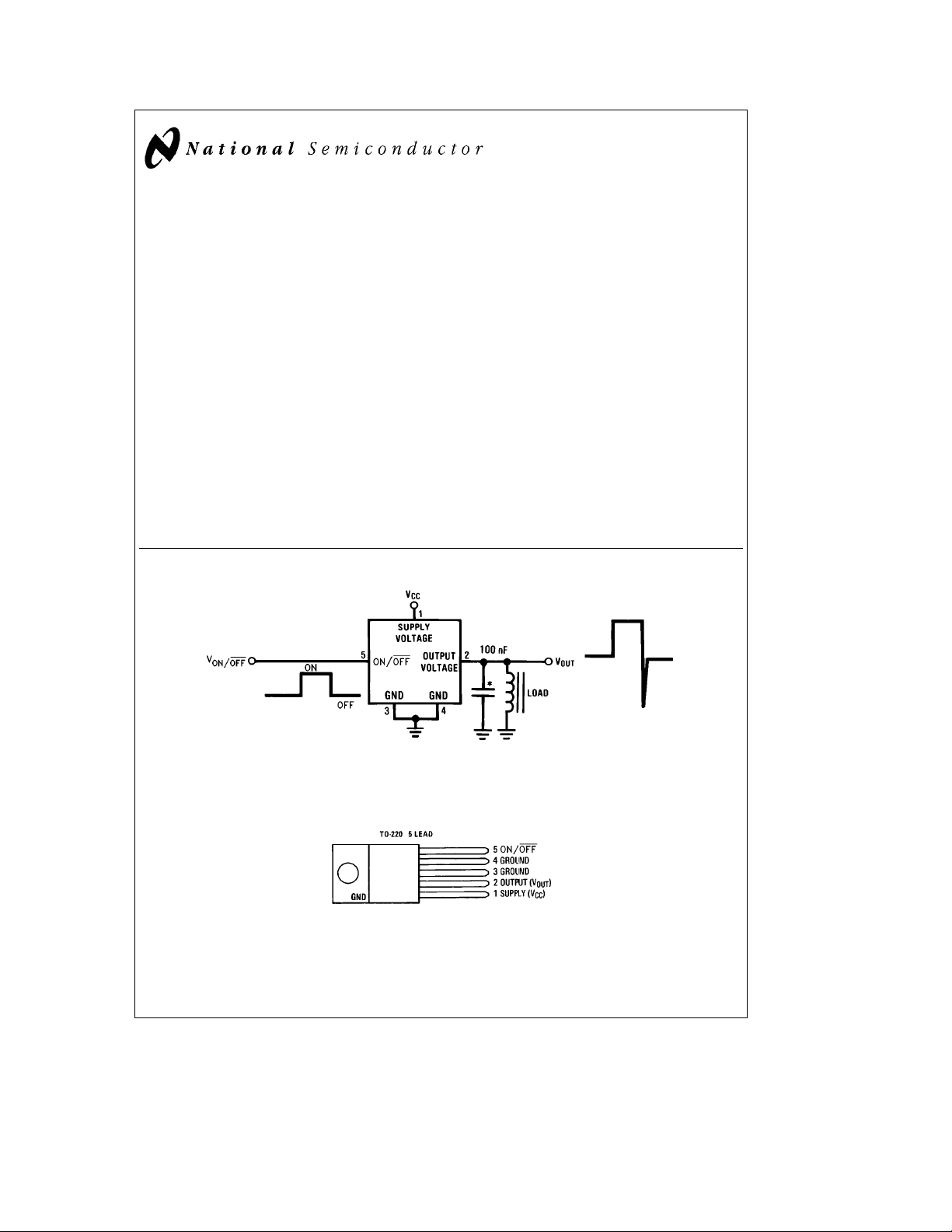
Typical Application Circuit
Features
Y
1 Amp output drive
Y
Load connected to ground
Y
Low input-output voltage differential
Y
a
60 volt positive transient protection
Y
b
50 volt negative transient protection
Y
Automotive reverse battery protection
Y
Short circuit proof
Y
Internal thermal overload protection
Y
Unclamped output for fast decay times
Y
TTL, LSTTL, CMOS compatible input
Y
Plastic TO-220 package
Y
100% electrical burn-in
Applications
Y
Relays
Y
Solenoids
Y
Valves
Y
Motors
Y
Lamps
Y
Heaters
*Required for stability
TL/H/5271– 1
FIGURE 1. Test and Application Circuit
Connection Diagram
Front View
Order Number LM1921T
See NS Package Number T05A
C
1995 National Semiconductor Corporation RRD-B30M115/Printed in U. S. A.
TL/H/5271
TL/H/5271– 2
Page 2
Absolute Maximum Ratings
If Military/Aerospace specified devices are required,
please contact the National Semiconductor Sales
Office/Distributors for availability and specifications.
Supply Voltage
Operating Range 4.75V to 26V
Overvoltage Protection (100 ms)
b
50V toa60V
Internal Power Dissipation Internally Limited
b
Operating Temperature Range
40§Ctoa125§C
Maximum Junction Temperature 150§C
Storage Temperature Range
b
65§Ctoa150§C
Lead Temp. (Soldering, 10 seconds) 230§C
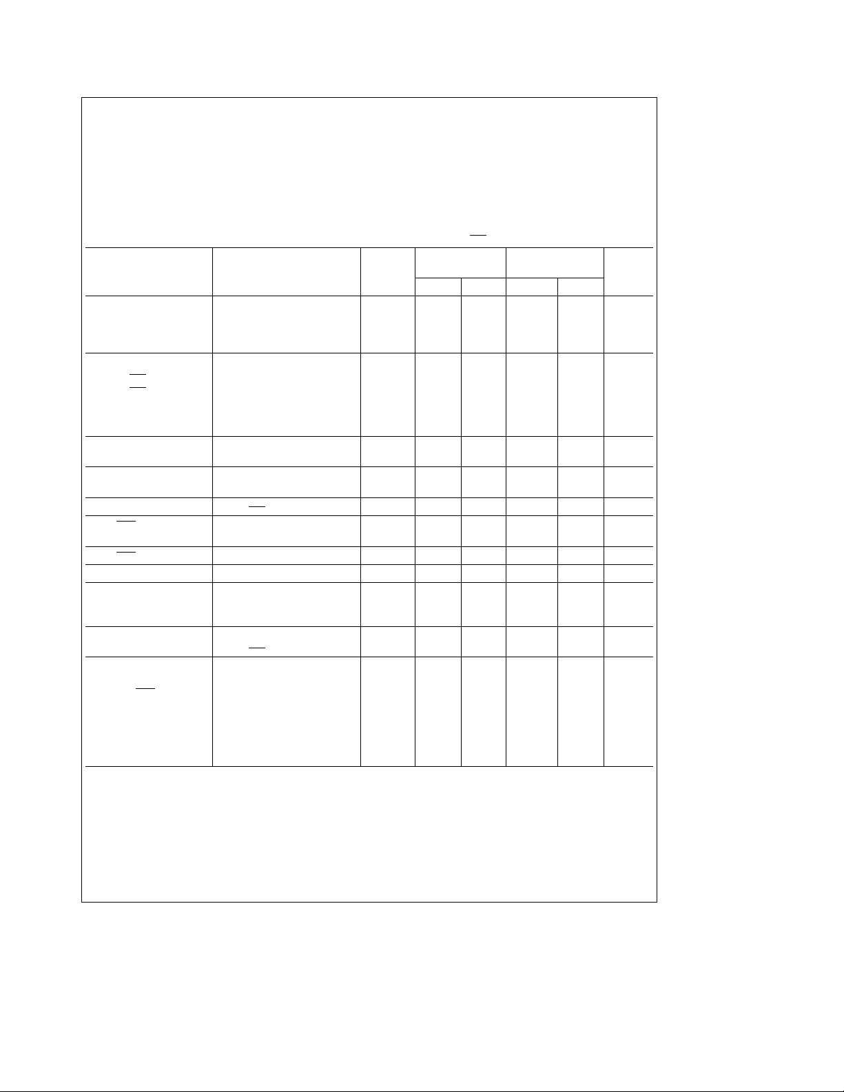
Electrical Characteristics (V
CC
e
12V, I
OUT
e
500 mA, T
e
J
25§C, V
ON/OFF
e
2V, unless otherwise specified.)
Tested Limits Design Limits
Parameter Conditions Typ
(Note 1) (Note 2)
Units
Min Max Min Max
Supply Voltage
Operational 4.75 26 6 24 V
Survival
Transient 100 ms, 1% Duty Cycle
b
15 60 V
b
50 V
Supply Current
e
V
ON/OFF
V
ON/OFF
Input to Output I
Voltage Drop I
0 0.6 1.5 mA
e
2V I
e
0 mA 6 10 mA
OUT
e
I
250 mA 285 350 mA
OUT
e
I
500 mA 575 700 mA
OUT
e
I
1A 1.3 1.5 A
OUT
e
500 mA 0.5 0.8 V
OUT
e
1A 1.0 V
OUT
Short Circuit Current 1.4 1.0 2.0 A
s
s
6V
V
24V .75 3.0 A
CC
Output Leakage Current V
ON/OFF
e
0 0.1 50 mA
ON/OFF Voltage 1.3 0.8 2.0 V
Threshhold 6VsV
s
24V 0.8 2.0 V
CC
ON/OFF Current 15 10 30 mA
Overvoltage Shutdown 32 26 36 V
Thermal Resistance
junction-case ijc 3
case-ambient ica 50
C/W
§
C/W
§
Inductive Clamp
Output Voltage V
ON/OFF
0, I
OUT
e
100 mA
b
60
b
120
b
45 V
e
Fault Conditions
Output Current
ON/OFF
Floating Pin 5 Open 0.1 50 mA
Ground Floating Pin 3 & Pin 4 Open 0.1 50 mA
Reverse Voltage V
Reverse Transient V
Overvoltage V
Supply Current Pin 1 & Pin 2 Short, No load 10 40 mA
Note 1: Guaranteed and 100% production tested.
Note 2: Guaranteed, not necessarily 100% production tested. Not used to calculate outgoing AQL . Limits are for the temperature range of
eb
15V
CC
eb
50V
CC
ea
60V 0.01 1 mA
CC
b
0.01
b
100 mA
b
1mA
b
40§CsT
j
s
150§C.
DC
2
Page 3

Typical Performance Characteristics
Output Voltage Drop
Device Operating Current
Peak Output Current (V
OUT
)
TL/H/5271– 3
Output Voltage Drop
TL/H/5271– 6
ON/OFF Current vs.
Junction Temperature
TL/H/5271– 13
Equivalent Block Diagram
Output Voltage (V
OUT
Threshold Voltage vs.
Supply Voltage
TL/H/5271– 4
)
TL/H/5271– 7
TL/H/5271– 14
Maximum Power
Dissipation (TO-220)
ON/OFF Current vs.
ON/OFF
Voltage
TL/H/5271– 5
TL/H/5271– 8
TL/H/5271– 15
FIGURE 1
3
TL/H/5271– 12
Page 4

Circuit Schematic
TL/H/5271– 9
4
Page 5

Application Hints
HIGH CURRENT OUTPUT
The 1 Amp output is fault protected against overvoltage. If
the supply voltage rises above approximately 30 volts, the
output will automatically shut down. This protects the internal circuitry and enables the IC to survive higher voltage
transients than would otherwise be expected. The 1921 will
survive transients and DC voltages up to 60 volts on the
supply. The output remains off during this time, independent
of the state of the input logic voltage. This protects the load.
The high current output is also protected against short circuits to either ground or supply voltage. Standard thermal
shutdown circuits are employed to protect the 1921 from
over heating.
FLYBACK RESPONSE
Since the 1921 is designed to drive inductive as well as any
other type of load, inductive kickback can be expected
whenever the output changes state from on to off (see
waveforms on
clamped since it is often desirable in many systems to
achieve a very rapid decay in the load current. In applications where this is not true, such as in
external diode clamp will suffice. In this application, the integrated current in the inductive load is controlled by varying
the duty cycle of the input to the driver IC. This technique
achieves response characteristics that are desirable for certain automotive transmission solenoids, for example.
For applications requiring a rapid controlled decay in the
solenoid current, such as fuel injector drivers, an external
zener and diode can be used as in
rating of the zener should be such that it breaks down before the output of the LM1921. The minimum output breakdown voltage of the IC output is rated at
respect to the supply voltage. Thus, on a 12 volt supply, the
Figure 1
). The driver output was left un-
Figure 3
Figure 2
. The voltage
b
57 volts with
, a simple
combined zener and diode breakdown should be less than
45 volts.
The LM1921 can be used alone as a simple relay or solenoid driver where a rapid decay of the load current is desired, but the exact rate of decay is not critical to the system. If the output is unclamped as in
Figure 1
, and the load
is inductive enough, the negative flyback transient will cause
the output of the IC to breakdown and behave similarly to a
zener clamp. Relying upon the IC breakdown is practical,
and will not damage or degrade the IC in any way. There are
two considerations that must be accounted for when the
driver is operated in this mode. The IC breakdown voltage is
process and lot dependent. Clamp voltages ranging from
b
60 tob120 volts (with respect to the supply voltage) will
be encountered over time on different devices. This is not at
all critical in most applications. An important consideration,
however, is the additional heat dissipated in the IC as a
result. This must be added to normal device dissipation
when considering junction temperatures and heat sinking
requirements. Worst case for the additional dissipation can
be approximated as:
e
I2xLxf(Watts)
D
where: I
Additional P
e
peak solenoid current (Amps)
Lesolenoid inductance (Henries)
femaximum frequency input signal (Hz)
For solenoids where the inductance is less than ten millihenries, the additional power dissipation can be ignored.
Overshoot, undershoot, and ringing can occur on certain
loads. The simple solution is to lower the Q of the load by
the addition of a resistor in parallel or series with the load. A
value that draws one tenth of the current or DC voltage of
the load is usually sufficient.
FIGURE 2. Diode Clamp
TL/H/5271– 10
FIGURE 3
TL/H/5271– 11
Zener clamp for rapid controlled current decay
5
Page 6

Physical Dimensions inches (millimeters)
LM1921 1 Amp Industrial Switch
5-Lead TO-220 Power Package (T)
Order Number LM1921T
NS Package Number T05A
LIFE SUPPORT POLICY
NATIONAL’S PRODUCTS ARE NOT AUTHORIZED FOR USE AS CRITICAL COMPONENTS IN LIFE SUPPORT
DEVICES OR SYSTEMS WITHOUT THE EXPRESS WRITTEN APPROVAL OF THE PRESIDENT OF NATIONAL
SEMICONDUCTOR CORPORATION. As used herein:
1. Life support devices or systems are devices or 2. A critical component is any component of a life
systems which, (a) are intended for surgical implant support device or system whose failure to perform can
into the body, or (b) support or sustain life, and whose be reasonably expected to cause the failure of the life
failure to perform, when properly used in accordance support device or system, or to affect its safety or
with instructions for use provided in the labeling, can effectiveness.
be reasonably expected to result in a significant injury
to the user.
National Semiconductor National Semiconductor National Semiconductor National Semiconductor
Corporation Europe Hong Kong Ltd. Japan Ltd.
1111 West Bardin Road Fax: (
Arlington, TX 76017 Email: cnjwge@tevm2.nsc.com Ocean Centre, 5 Canton Rd. Fax: 81-043-299-2408
Tel: 1(800) 272-9959 Deutsch Tel: (
Fax: 1(800) 737-7018 English Tel: (
National does not assume any responsibility for use of any circuitry described, no circuit patent licenses are implied and National reserves the right at any time without notice to change said circuitry and specifications.
Fran3ais Tel: (
Italiano Tel: (
a
49) 0-180-530 85 86 13th Floor, Straight Block, Tel: 81-043-299-2309
a
49) 0-180-530 85 85 Tsimshatsui, Kowloon
a
49) 0-180-532 78 32 Hong Kong
a
49) 0-180-532 93 58 Tel: (852) 2737-1600
a
49) 0-180-534 16 80 Fax: (852) 2736-9960
 Loading...