

Page 1
©2001 Fairchild Semiconductor Corporation
www.fairchildsemi.com
Rev. 1.0.1
Features
• Internal frequency compensation
• Short circuit protecion
• Large common mode and differential voltage range
• No latch up
• Low power consumption
Description
The LM1458/LM1458C series are dual general purpose
operational amplifiers, having short circuits protected and
require no external components for frequency
compensation. High common mode voltage range and
absence of “latch up" make the LM1458 ideal for use as
voltage follower s. The hi gh ga in an d wide r ange of ope ratin g
voltage provides superior performance in integrator,
summing amplifier and general feedback applications.
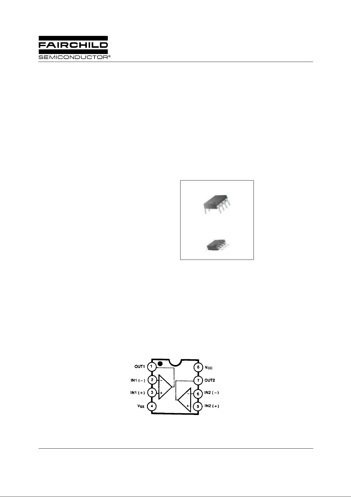
8-DIP
8-SOP
1
1
Internal Block Diagram
LM1458/LM1458C
Dual Operational Amplifier
Page 2
LM1458/LM1458C
2
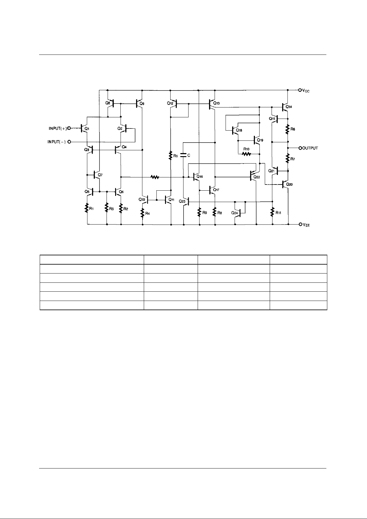
Schematic Diagram
Absolute Maximum Ratings
Parameter Symbol Value Unit
Power Supply Voltage V
CC
±18 V
Input Differential Voltage V
I(DIFF)
30 V
Input Voltage V
I
±15 V
Operating Temperature Range T
OPR
0 ~ + 70 °C
Storage Temperature Range T
STG
- 65 ~ + 150 °C
Page 3
LM1458/LM1458C
3
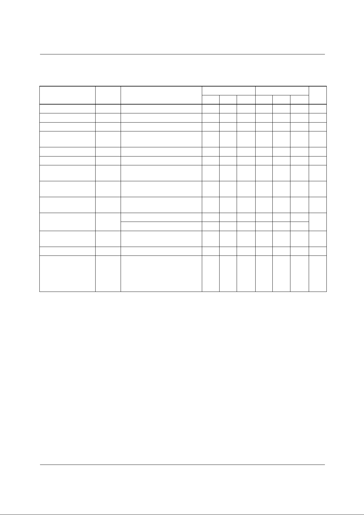
Electrical Characteristics
(VCC = + 15V, VEE = - 15V, TA = 25 °C unless otherwise specified)
Parameter Symbol Conditions
LM1458C LM1458
Unit
Min. Typ. Max. Min. Typ. Max.
Input Offset Voltage V
IO
R
S
≤10KΩ - 2.0 10 - 2.0 6.0 mV
Input Offset Current I
IO
- - 20 300 - 20 200 nA
Input Bias Current I
BIAS
- - 80 700 - 80 500 nA
Large Signal
Voltage Gain
G
V
V
O(P-P)
= ± 10V, R
L
≥2.0KΩ 20 200 - 20 200 - V/mV
Input Voltage Range V
I(R)
- ± 11 ± 13 - ± 12 ± 13 - V
Input Resistance R
I
- 0.3 1.0 - 0.3 1.0 - MΩ
Common Mode
Rejection Ratio
CMRR - 60 90 - 70 90 - dB
Power Supply
Rejection Ratio
PSRR - 77 90 - 77 90 - dB
Supply Current
(Both Amplifier)
I
CC
--2.38.0-2.3-mA
Output Voltage
Swing
V
O(PP)
R
S
≤10KΩ± 11 ± 14 - ± 12 ± 14 5.6
V
R
S
≤10KΩ± 19 ± 13 - ± 10 ± 13 -
Output Short Circuit
Current
I
SC
- - 20 - - 20 - mA
Power Consumption P
C
VO = 0V - 70 240 - 70 170 mW
Transient Response
(Unity Gain)
Rise Time
Overshoot
Slew Rate
T
R
OS
SR
V
I
= 20mV,R
L
≥2KΩ,CL≤100pF
V
I
= 20mV,R
L
≥2KΩ,CL≤100pF
V
I
= 10V,R
L
≥2KΩ,CL≤100pF
-0.3
15
0.5
--0.3
15
0.5
- µs
%
V/µs
Page 4

LM1458/LM1458C
4
Electrical Characteristics
(VCC = + 15V, VEE = - 15V, Note1, unless otherwise specified)
Note :
1. LM1458/LM1458C : 0°C ≤T
A
≤70°C
Parameter Symbol Conditions
LM1458C LM1458
Unit
Min. Typ. Max. Min. Typ. Max.
Input Offset Voltage V
IO
R
S
≤10KΩ - - 12 - - 7.5 mV
Input Offset Current I
IO
- - - 400 - - 300 nA
Input Bias Current I
BIAS
- - - 1000 - - 800 nA
Large Signal Voltage
Gain
G
V
V
O(P-P)
= ± 10V, R
L
≤2.0KΩ 15 - - 15 - - V/mV
Common Mode
Rejection Ratio
CMRR R
S
≥10KΩ 70 90 - 70 90 - dB
Power Supply
Rejection Ratio
PSRR R
S
≥10KΩ 77 90 - 77 90 - dB
Output Voltage Swing V
O(P.P)
RL = 10KΩ± 11 ± 14 - ± 12 ± 14 - V
R
L
= 2KΩ± 9 ± 13 - ± 10 ± 13 -
Input Voltage Range V
I(R)
- ± 12 - - ± 12 - - V
Page 5

LM1458/LM1458C
5
Typical Performance Characteristics
Figure 1. Open-Loop Voltage Gain vs
Power Supply Voltages
Figure 2. Open-Loop Frequency Response
Figure 3. Power Bandwidth
(Large Signal Output Swing vs Frequency)
Figure 4. Output Voltage Swing vs Load Resistance
Page 6

LM1458/LM1458C
6
Mechanical Dimensions
Package
6.40 ±0.20
3.30 ±0.30
0.130 ±0.012
3.40 ±0.20
0.134 ±0.008
#1
#4 #5
#8
0.252
±0.008
9.20 ±0.20
0.79
2.54
0.100
0.031
()
0.46
±0.10
0.018 ±0.004
0.060 ±0.004
1.524 ±0.10
0.362 ±0.008
9.60
0.378
MAX
5.08
0.200
0.33
0.013
7.62
0~15°
0.300
MAX
MIN
0.25
+0.10
–0.05
0.010
+0.004
–0.002
8-DIP
Page 7

LM1458/LM1458C
7
Mechanical Dimensions
(Continued)
Package
4.92 ±0.20
0.194 ±0.008
0.41 ±0.10
0.016 ±0.004
1.27
0.050
5.72
0.225
1.55 ±0.20
0.061 ±0.008
0.1~0.25
0.004~0.001
6.00 ±0.30
0.236 ±0.012
3.95 ±0.20
0.156 ±0.008
0.50 ±0.20
0.020 ±0.008
5.13
0.202
MAX
#1
#4
#5
0~8°
#8
0.56
0.022
()
1.80
0.071
MAX0.10
MAX0.004
MAX
MIN
+
0.10
-0.05
0.15
+
0.004
-0.002
0.006
8-SOP
Page 8

LM1458/LM1458C
8
Ordering Information
Product Number Package Operating Temperature
LM1458CN
8-DIP
0 ~ + 70°C
LM1458N
LM1458CM
8-SOP
LM1458M
Page 9

LM1458/LM1458C
9
Page 10

LM1458/LM1458C
6/1/01 0.0m 001
Stock#DSxxxxxxxx
2001 Fairchild Semiconductor Corporation
LIFE SUPPORT POL I CY
FAIRCHILD’S PRODUCTS ARE NOT AUTHORIZED FOR USE AS CRITICAL COMPONENTS IN LIFE SUPPORT DEVICES
OR SYSTEMS WITHOUT THE EXPRESS WRITTEN APPROVAL OF THE PRESIDENT OF FAIRCHILD SEMICONDUCTOR
CORPORATION. As used herein :
1. Life support devices or systems are devices or systems
which, (a) are intended for surgical implant into the body,
or (b) support or sustain life, and (c) whose failure to
perform when properly used in accordance with
instructions for use provided in the labeling, can be
reasonably expected to result in a significant injury of the
user.
2. A critical component in any component of a life support
device or sys tem whose failure to perform can be
reasonably expec ted to cause the failur e of the life support
device or system, or to affect its safety or effec tiveness.
www.fairchildsemi.com
DISCLAIMER
FAIRCHILD SEMICONDUCTOR RESERVES THE RIGHT TO MAKE CHANGES WITHOUT FURTHER NOTICE TO ANY
PRODUCTS HEREI N TO IMPROVE RELIABILITY, FUNCTION OR DES IGN. FAIRCHILD DOES NOT ASSUME ANY
LIABILITY ARISING OUT OF THE APPLICATION OR USE OF ANY PRODUCT OR CIRCUIT DESCRIBED HEREIN; NEITHER
DOES IT CONVEY ANY LICENSE UNDER ITS PATENT RIGHTS, NOR THE RI GHTS OF OTHERS.
 Loading...