

Page 1
FAMILY OF JFET
OPERATIONAL AMPLIFIERS
Order this document by LF347/D
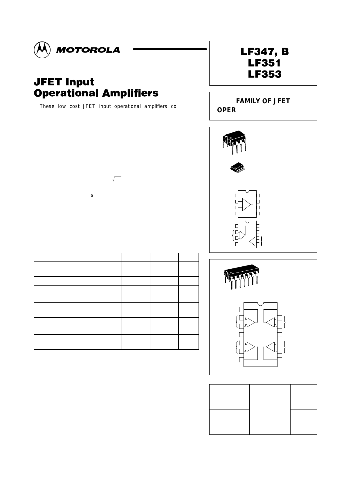
D SUFFIX
PLASTIC PACKAGE
CASE 751
(SO–8)
N SUFFIX
PLASTIC PACKAGE
CASE 626
Output A
Inputs A
V
EE
V
CC
Output B
Inputs B
LF351
(Top View)
LF353
(Top View)
Offset Null
Invt Input
Noninvt Input
V
EE
NC
V
CC
Output
Offset Null
1
2
3
4
8
7
6
5
+
–
–
–
+
+
A
B
1
2
3
4
8
7
6
5
1
1
8
8
PIN CONNECTIONS
N SUFFIX
PLASTIC PACKAGE
CASE 646
(Top View)
Out 1
Inputs 1
V
CC
Inputs 2
Out 2
Out 4
Inputs 4
V
EE
Inputs 3
Out 3
1
2
3
4
5
6
78
9
10
11
12
13
14
4
23
++
++
1
––
––
14
1
PIN CONNECTIONS
ORDERING INFORMATION
FunctionDevice Package
Operating
Temperature Range
LF351D
LF351N
Single
Single
TA = 0° to +70°C
SO–8
Plastic DIP
LF353D
LF353N
Dual
Dual
SO–8
Plastic DIP
LF347BN
LF347N
Quad
Quad
Plastic DIP
Plastic DIP
1
MOTOROLA ANALOG IC DEVICE DATA
These low cost JFET input operational amplifiers combine two
state–of–the–art analog technologies on a single monolithic integrated
circuit. Each internally compensated operational amplifier has well matched
high voltage JFET input devices for low input offset voltage. The JFET
technology provides wide bandwidths and fast slew rates with low input bias
currents, input offset currents, and supply currents.
These devices are available in single, dual and quad operational
amplifiers which are pin–compatible with the industry standard MC1741,
MC1458, and the MC3403/LM324 bipolar devices.
• Input Offset Voltage of 5.0 mV Max (LF347B)
• Low Input Bias Current: 50 pA
• Low Input Noise Voltage: 16 nV/ Hz
Ǹ
• Wide Gain Bandwidth: 4.0 MHz
• High Slew Rate: 13V/µs
• Low Supply Current: 1.8 mA per Amplifier
• High Input Impedance: 10
12
Ω
• High Common Mode and Supply Voltage Rejection Ratios: 100 dB
MAXIMUM RATINGS
Rating Symbol Value Unit
Supply Voltage V
CC
+18 V
V
EE
–18
Differential Input Voltage V
ID
±30 V
Input Voltage Range (Note 1) V
IDR
±15 V
Output Short Circuit Duration (Note 2) t
SC
Continuous
Power Dissipation at TA = +25°C P
D
900 mW
Derate above TA =+25°C 1/
θJA
10 mW/°C
Operating Ambient Temperature Range T
A
0 to +70 °C
Operating Junction Temperature Range T
J
115 °C
Storage Temperature Range T
stg
– 65 to
+150
°C
NOTES: 1.Unless otherwise specified, the absolute maximum negative input voltage is
limited to the negative power supply.
2.Any amplifier output can be shorted to ground indefinitely. However , if more than
one amplifier output is shorted simultaneously, maximum junction temperature
rating may be exceeded.
Motorola, Inc. 1996 Rev 0
Page 2
LF347, B LF351 LF353
2
MOTOROLA ANALOG IC DEVICE DATA
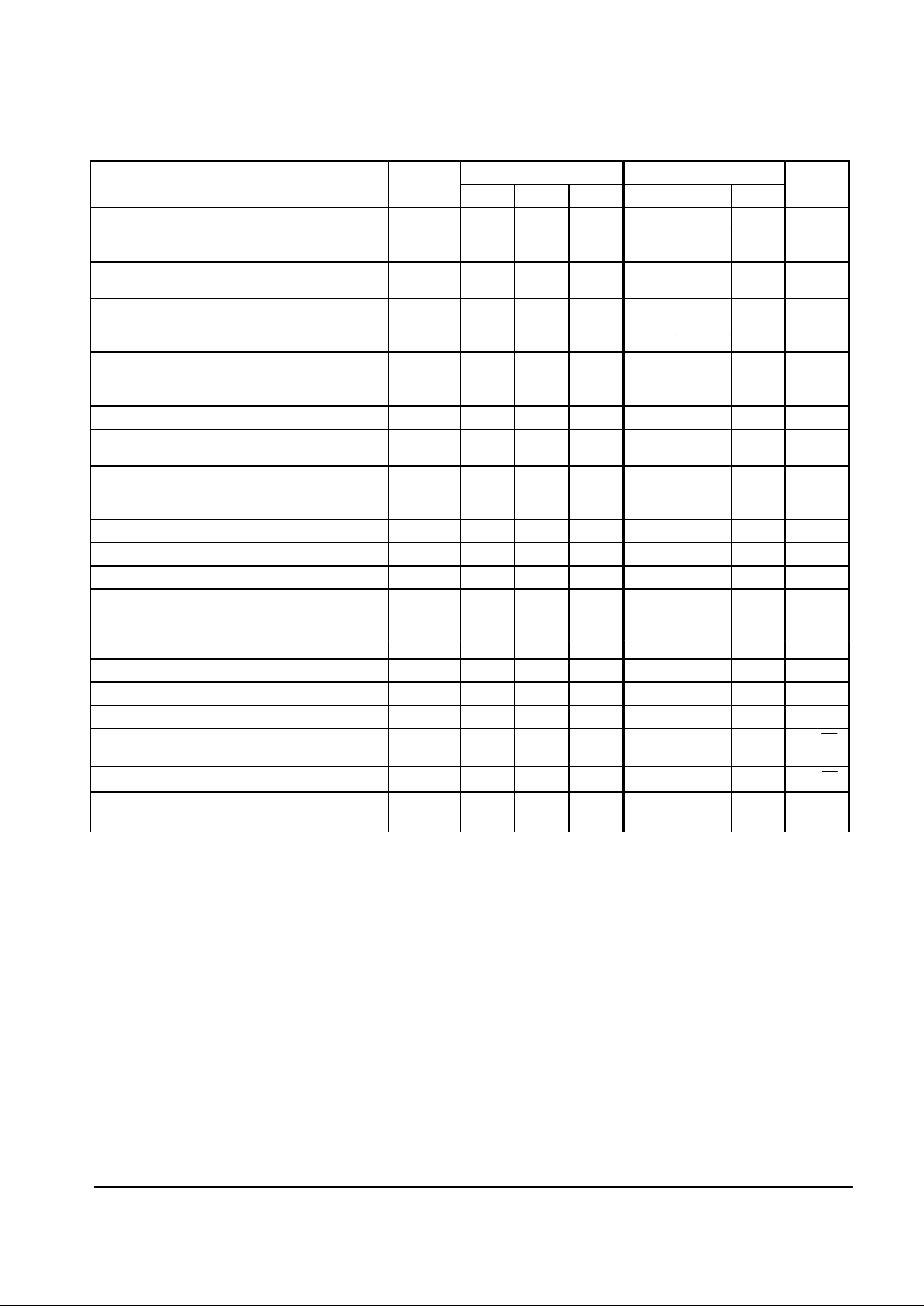
ELECTRICAL CHARACTERISTICS
(VCC = +15 VEE = –15 V , TA = 25°C, unless otherwise noted.)
LF347B LF347, LF351, LF353
Characteristic Symbol
Min Typ Max Min Typ Max
Unit
Input Offset Voltage (RS ≤ 10 k, VCM = 0) V
IO
mV
TA = +25°C – 1.0 5.0 – 5.0 10
0°C ≤ TA ≤ +70°C – – 8.0 – – 13
Avg. Temperature Coefficient of Input Offset Voltage ∆VIO/∆T µV/°C
RS ≤ 10 k, 0°C ≤ TA ≤ +70°C – 10 – – 10 –
Input Offset Current (VCM = 0, Note 3) I
IO
TA = +25°C – 25 100 – 25 100 pA
0°C ≤ TA ≤ +70°C – – 4.0 – – 4.0 nA
Input Bias Current (VCM = 0, Note 3) I
IB
TA = +25°C – 50 200 – 50 200 pA
0°C ≤ TA ≤ +70°C – – 8.0 – – 8.0 nA
Input Resistance r
i
– 10
12
– – 10
12
– Ω
Common Mode Input Voltage Range V
ICR
±11 +15 – ±11 +15 – V
–12 –12
Large–Signal Voltage Gain (VO = ±10 V, RL = 2.0 k) A
VOL
V/mV
TA = +25°C 50 100 – 25 100 –
0°C ≤ TA ≤ +70°C 25 – – 15 – –
Output Voltage Swing (RL = 10 k) V
O
±12 ±14 – ±12 ±14 – V
Common Mode Rejection (RS ≤ 10 k) CMR 80 100 – 70 100 – dB
Supply Voltage Rejection (RS ≤ 10 k) PSRR 80 100 – 70 100 – dB
Supply Current I
D
mA
LF347 – 7.2 11 – 7.2 11
LF351 – – – – 1.8 3.4
LF353 – – – – 3.6 6.5
Short Circuit Current I
SC
– 25 – – 25 – mA
Slew Rate (AV = +1) SR – 13 – – 13 – V/µs
Gain–Bandwidth Product BWp – 4.0 – – 4.0 – MHz
Equivalent Input Noise Voltage e
n
– 24 – – 24 –
nV/ Hz√
(RS = 100 Ω, f = 1000 Hz)
Equivalent Input Noise Current (f = 1000 Hz) i
n
– 0.01 – – 0.01 –
pA/ Hz√
Channel Separation (LF347, LF353) – – –120 – – –120 – dB
1.0 Hz ≤ f ≤ 20 kHz (Input Referred)
For Typical Characteristic Performance Curves, refer to MC34001, 34002, 34004 data sheet.
NOTE: 3.Input bias currents of JFET input op amps approximately double for every 10°C rise in junction temperature. T o maintain junction temperatures as
close to ambient as is possible, pulse techniques are utilized during test.
Page 3

LF347, B LF351 LF353
3
MOTOROLA ANALOG IC DEVICE DATA
OUTLINE DIMENSIONS
NOTES:
1. DIMENSION L TO CENTER OF LEAD WHEN
FORMED PARALLEL.
2. PACKAGE CONTOUR OPTIONAL (ROUND OR
SQUARE CORNERS).
3. DIMENSIONING AND TOLERANCING PER ANSI
Y14.5M, 1982.
14
58
F
NOTE 2
–A–
–B–
–T–
SEATING
PLANE
H
J
G
D
K
N
C
L
M
M
A
M
0.13 (0.005) B
M
T
DIM MIN MAX MIN MAX
INCHESMILLIMETERS
A 9.40 10.16 0.370 0.400
B 6.10 6.60 0.240 0.260
C 3.94 4.45 0.155 0.175
D 0.38 0.51 0.015 0.020
F 1.02 1.78 0.040 0.070
G 2.54 BSC 0.100 BSC
H 0.76 1.27 0.030 0.050
J 0.20 0.30 0.008 0.012
K 2.92 3.43 0.115 0.135
L 7.62 BSC 0.300 BSC
M ––– 10 ––– 10
N 0.76 1.01 0.030 0.040
__
D SUFFIX
PLASTIC PACKAGE
CASE 751–05
(SO–8)
ISSUE R
N SUFFIX
PLASTIC PACKAGE
CASE 626–05
ISSUE K
SEATING
PLANE
1
4
58
A0.25MCB
SS
0.25MB
M
h
q
C
X 45
_
L
DIM MIN MAX
MILLIMETERS
A 1.35 1.75
A1 0.10 0.25
B 0.35 0.49
C 0.18 0.25
D 4.80 5.00
E
1.27 BSCe
3.80 4.00
H 5.80 6.20
h
0 7
L 0.40 1.25
q
0.25 0.50
__
NOTES:
1. DIMENSIONING AND TOLERANCING PER ASME
Y14.5M, 1994.
2. DIMENSIONS ARE IN MILLIMETERS.
3. DIMENSION D AND E DO NOT INCLUDE MOLD
PROTRUSION.
4. MAXIMUM MOLD PROTRUSION 0.15 PER SIDE.
5. DIMENSION B DOES NOT INCLUDE MOLD
PROTRUSION. ALLOWABLE DAMBAR
PROTRUSION SHALL BE 0.127 TOTAL IN EXCESS
OF THE B DIMENSION AT MAXIMUM MATERIAL
CONDITION.
D
E
H
A
B
e
B
A1
C
A
0.10
Page 4

LF347, B LF351 LF353
4
MOTOROLA ANALOG IC DEVICE DATA
OUTLINE DIMENSIONS
NOTES:
1. LEADS WITHIN 0.13 (0.005) RADIUS OF TRUE
POSITION AT SEATING PLANE AT MAXIMUM
MATERIAL CONDITION.
2. DIMENSION L TO CENTER OF LEADS WHEN
FORMED PARALLEL.
3. DIMENSION B DOES NOT INCLUDE MOLD
FLASH.
4. ROUNDED CORNERS OPTIONAL.
17
14 8
B
A
F
HG D
K
C
N
L
J
M
SEATING
PLANE
DIM MIN MAX MIN MAX
MILLIMETERSINCHES
A 0.715 0.770 18.16 19.56
B 0.240 0.260 6.10 6.60
C 0.145 0.185 3.69 4.69
D 0.015 0.021 0.38 0.53
F 0.040 0.070 1.02 1.78
G 0.100 BSC 2.54 BSC
H 0.052 0.095 1.32 2.41
J 0.008 0.015 0.20 0.38
K 0.115 0.135 2.92 3.43
L 0.300 BSC 7.62 BSC
M 0 10 0 10
N 0.015 0.039 0.39 1.01
____
N SUFFIX
PLASTIC PACKAGE
CASE 646–06
ISSUE L
Motorola reserves the right to make changes without further notice to any products herein. Motorola makes no warranty , representation or guarantee regarding
the suitability of its products for any particular purpose, nor does Motorola assume any liability arising out of the application or use of any product or circuit, and
specifically disclaims any and all liability, including without limitation consequential or incidental damages. “T ypical” parameters which may be provided in Motorola
data sheets and/or specifications can and do vary in different applications and actual performance may vary over time. All operating parameters, including “Typicals”
must be validated for each customer application by customer’s technical experts. Motorola does not convey any license under its patent rights nor the rights of
others. Motorola products are not designed, intended, or authorized for use as components in systems intended for surgical implant into the body, or other
applications intended to support or sustain life, or for any other application in which the failure of the Motorola product could create a situation where personal injury
or death may occur. Should Buyer purchase or use Motorola products for any such unintended or unauthorized application, Buyer shall indemnify and hold Motorola
and its officers, employees, subsidiaries, affiliates, and distributors harmless against all claims, costs, damages, and expenses, and reasonable attorney fees
arising out of, directly or indirectly, any claim of personal injury or death associated with such unintended or unauthorized use, even if such claim alleges that
Motorola was negligent regarding the design or manufacture of the part. Motorola and are registered trademarks of Motorola, Inc. Motorola, Inc. is an Equal
Opportunity/Affirmative Action Employer.
How to reach us:
USA/EUROPE/Locations Not Listed: Motorola Literature Distribution; JAPAN: Nippon Motorola Ltd.; Tatsumi–SPD–JLDC, 6F Seibu–Butsuryu–Center,
P.O. Box 20912; Phoenix, Arizona 85036. 1–800–441–2447 or 602–303–5454 3–14–2 Tatsumi Koto–Ku, Tokyo 135, Japan. 03–81–3521–8315
MFAX: RMF AX0@email.sps.mot.com – TOUCHT ONE 602–244–6609 ASIA/PACIFIC: Motorola Semiconductors H.K. Ltd.; 8B Tai Ping Industrial Park,
INTERNET: http://Design–NET.com 51 Ting Kok Road, Tai Po, N.T., Hong Kong. 852–26629298
LF347/D
*LF347/D*
◊
 Loading...