

Page 1
DEVICES INCORPORATED
LF3370
High-Definition Video Format Converter
LF3370
DEVICES INCORPORATED
FEATURES
❑❑
❑ 83 MHz Data Rate for HDTV
❑❑
Applications
❑❑
❑ Supports Multiple Video Formats
❑❑
Bi-Directional Conversions:
- 4:2:2:4
- 4:4:4:4
- R/G/B/Key
- Y/U/V/Key
❑❑
❑ Multiplexed and Non-multiplexed
❑❑
I/O Data
❑❑
❑ User-Programmable:
❑❑
- 3 x 3 Colorspace Converter
- LUT for Gamma Correction
- I/O Bias Compensation
- Bypass Capability
❑❑
❑ 13-bit Data Path, Colorspace
❑❑
Converter Coefficients and Key
Channel Scaling Coefficients
❑❑
❑ 160-lead PQFP
❑❑
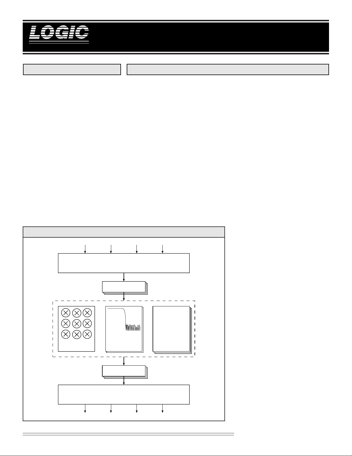
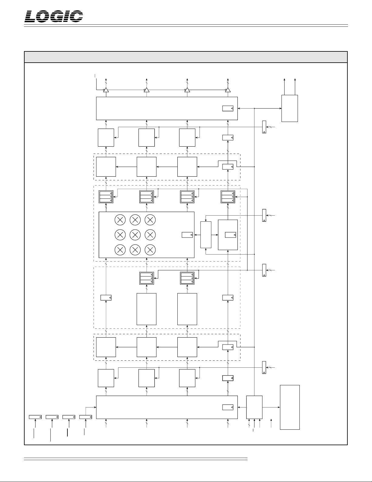
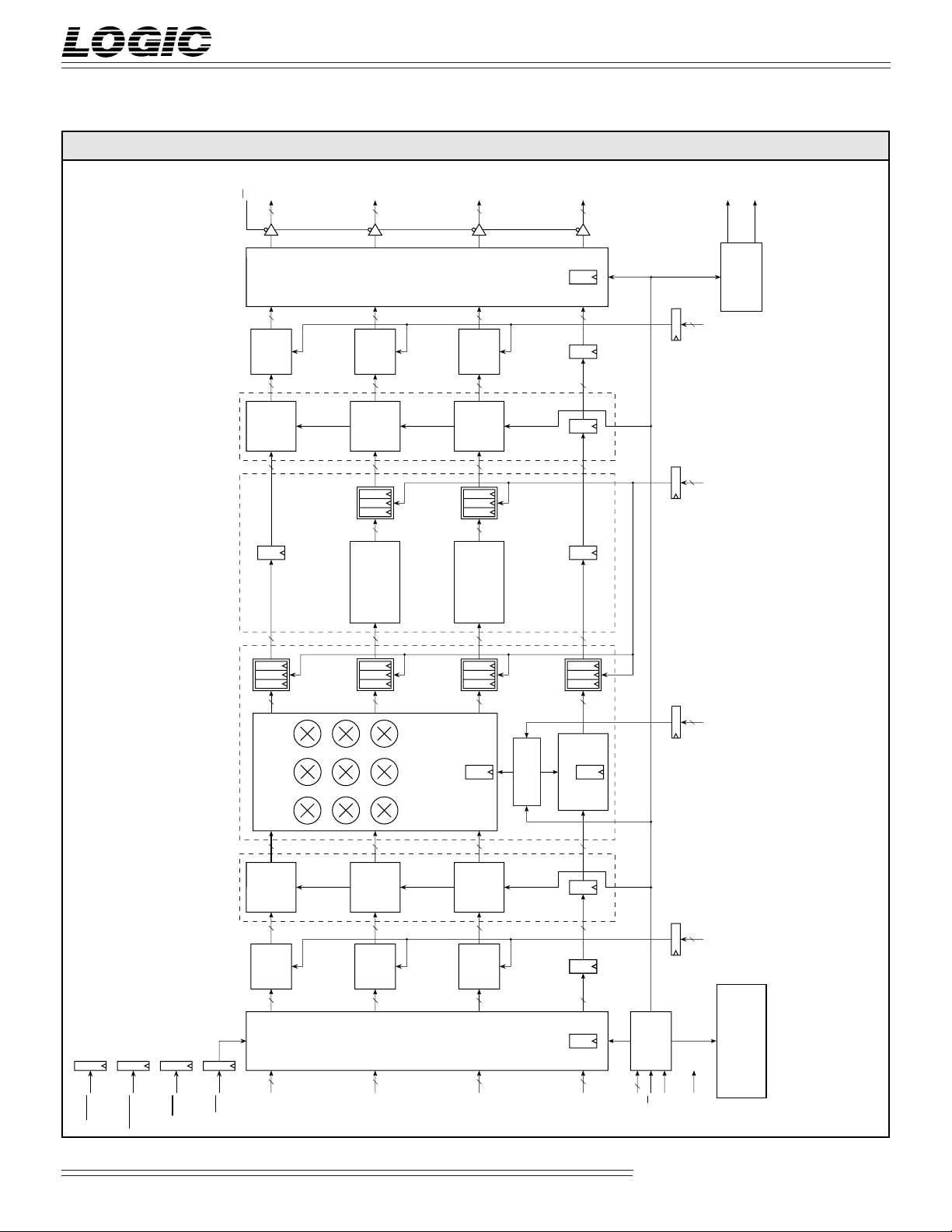
LF3370 BLOCK DIAGRAM
B
A
12-0
12-0
INPUT DE-MULTIPLEXER SECTION
INPUT BIAS ADDERS
High-Definition Video Format Converter
DESCRIPTION
The LF3370 is a video format
converter capable of operating at
HDTV data rates. This device
converts to and from any of the
various SDTV/HDTV digital video
formats by utilizing an internal
3 x 3 Matrix Multiplier and two
1:2 Interpolation/2:1 Decimation
Half-Band Filters.
Using the Input Demultiplexer
and Output Multiplexer, the
LF3370 can accept and output
interleaved or non-interleaved
video. For example, R/G/B/Key
data can be color space converted
to Y/U/V/Key and down-converted to 4:2:2:4. By re-arranging
the order of the functional sections, the opposite conversion can
be achieved. The coefficients for
C
12-0
D
12-0
the 3 x 3 Matrix Multiplier are
fully user programmable to support a wide range of color space
conversions. The two Interpolation/Decimation Half-Band Filters
are fully compliant with SMPTE
260M.
Input and Output Bias Adders are
included for removing or adding a
user-defined bias into the video
signal. In addition, three programmable 1K x 13-bit Look-Up
Tables (LUTs) have also been
included for various uses such as
gamma correction. A Scaler has
been included on the Key Channel
for scaling to a desired magnitude
using user programmable coefficients.
Input signals can also be forced to
user-defined levels for horizontal
blanking. Furthermore, Round/
Select/Limit (RSL) circuitry is
provided at the end of various
stages to provide the best possible
conversions without color violations. For additional flexibility,
the Halfband Filter can be individually bypassed using an internal programmable length delay.
All control and coefficient registers
are loaded through the LF Interface™.
COLORSPACE
CONVERTER/
KEY SCALER
W
12-0
55-TAP HALF-BAND
INTERPOLATION/
DECIMATION
FILTERS
OUTPUT BIAS ADDERS
OUTPUT MULTIPLEXER SECTION
X
12-0
Y
12-0
1K x 13-Bit
LOOK-UP-TABLES
Z
12-0
1
This device operates at 3.3 V (5 V
tolerant I/O) and is available in
160-lead PQFP package.
Video Imaging Products
03/13/2001–LDS.3370-F
Page 2
DEVICES INCORPORATED
High-Definition Video Format Converter
FIGURE 1. LF3370 FUNCTIONAL BLOCK DIAGRAM (HALF-BAND FILTER TO COLORSPACE ARRANGEMENT)
12-0
OE
WOUT
13
12-0
XOUT
13
12-0
YOUT
13
12-0
ZOUT
13
HF0HF
1
LF3370
13
BIAS
ADDER
OUTPUT
13
LUT*
1K x 13-bit
13
LIMIT
SELECT
ROUND
20
3 X 3 MATRIX MULTIPLY / KEY SCALER
35
13
BIAS
ADDER
OUTPUT
13
LUT*
1K x 13-bit
LIMIT
SELECT
ROUND
20 13
LIMIT
SELECT
ROUND
20 13
MUX
OUTPUT
CONVERTER
COLORSPACE
13
BIAS
ADDER
OUTPUT
13
LUT*
1K x 13-bit
LIMIT
SELECT
ROUND
20 13
3
LIMIT
SELECT
ROUND
20 13
BANKS 0-9
KEY SCALER
COEFFICIENT
23-5
13
1
13
2
13
LIMIT
SELECT
ROUND
20
3
13
35
FLAG
GENERATOR
1-0
OUTBIAS
1-0
2 2
CA
1-0
2
RSL
HBLANK
DATAPASS
RESET
CHROMA HALF-BAND FILTER / INTERPOLATOR
13
LUT*
1K x 13-bit
INPUT LOOK-UP-TABLE* OUTPUT LOOK-UP-TABLE*
13
BIAS
INPUT
ADDER
13 13
13
SYNC
12-0
AIN
FILTER/
HALF-BAND
INTERPOLATOR
13
LUT*
1K x 13-bit
13
BIAS
INPUT
ADDER
13
13
12-0
BIN
INPUT
DEMUX
FILTER/
HALF-BAND
INTERPOLATOR
13
LUT*
1K x 13-bit
13
BIAS
INPUT
ADDER
13
13
12-0
CIN
2
13
2
13
1
13
1-0
2
INBIAS
LF
INTERFACE
13
12-0
DIN
13
LD
12-0
CF
PAUSE
CONFIGURATION AND
CLK
CONTROL REGISTERS
TO NUMBER OF PIPELINE DELAYS THROUGH THAT PARTICULAR FUNCTIONAL BLOCK
THE LOOK-UP-TABLE IS TWO REGARDLESS OF WHETHER IT IS USED OR NOT.
* UP TO ONE LOOK-UP-TABLE MAY BE USED PER DATA PATH. THE INHERENT DELAY THROUGH
NOTE: NUMBERS IN REGISTERS INDICATE NUMBER OF PIPELINE DELAYS WHICH IS ALSO EQUIVALENT
Video Imaging Products
03/13/2001–LDS.3370-F
Page 3
DEVICES INCORPORATED
High-Definition Video Format Converter
FIGURE 2. LF3370 FUNCTIONAL BLOCK DIAGRAM (COLORSPACE TO HALF-BAND FILTER ARRANGEMENT)
12-0
OE
WOUT
13
12-0
XOUT
13
12-0
YOUT
13
12-0
ZOUT
13
HF0HF
1
LF3370
13
BIAS
ADDER
OUTPUT
13
LUT*
1K x 13-bit
13
35
HALF-BAND
CHROMA HALF-BAND FILTER / INTERPOLATOR
13
LIMIT
SELECT
ROUND
20
13
BIAS
ADDER
OUTPUT
13
LUT*
1K x 13-bit
13
LIMIT
SELECT
ROUND
20
FILTER/
DECIMATOR
13
LIMIT
SELECT
ROUND
20
MUX
OUTPUT
13
BIAS
ADDER
OUTPUT
13
LUT*
1K x 13-bit
13
LIMIT
SELECT
ROUND
20
FILTER/
HALF-BAND
DECIMATOR
13
LIMIT
SELECT
ROUND
20
23-5
13
1
13
2
13
35
13
LIMIT
SELECT
ROUND
20
FLAG
GENERATOR
1-0
2
OUTBIAS
1-0
2
RSL
1-0
2
CA
HBLANK
DATAPASS
RESET
3 X 3 MATRIX MULTIPLY / KEY SCALER
13
LUT*
1K x 13-bit
INPUT LOOK-UP-TABLE* OUTPUT LOOK-UP-TABLE*
13
BIAS
INPUT
ADDER
13
13
SYNC
12-0
AIN
13
LUT*
1K x 13-bit
13
BIAS
INPUT
ADDER
13
13
12-0
BIN
CONVERTER
COLORSPACE
INPUT
DEMUX
3
13
LUT*
1K x 13-bit
13
BIAS
INPUT
ADDER
13
13
12-0
CIN
3
BANKS 0-9
KEY SCALER
COEFFICIENT
3
13
2
13
1
13
1-0
2
INBIAS
LF
INTERFACE
13
12-0
DIN
13
LD
12-0
CF
PAUSE
CONFIGURATION AND
CLK
CONTROL REGISTERS
TO NUMBER OF PIPELINE DELAYS THROUGH THAT PARTICULAR FUNCTIONAL BLOCK
THE LOOK-UP-TABLE IS TWO REGARDLESS OF WHETHER IT IS USED OR NOT.
* UP TO ONE LOOK-UP-TABLE MAY BE USED PER DATA PATH. THE INHERENT DELAY THROUGH
NOTE: NUMBERS IN REGISTERS INDICATE NUMBER OF PIPELINE DELAYS WHICH IS ALSO EQUIVALENT
Video Imaging Products
03/13/2001–LDS.3370-F
Page 4

DEVICES INCORPORATED
LF3370
High-Definition Video Format Converter
SIGNAL DEFINITIONS
Power
VCC and GND
+3.3 V power supply. All power pins
must be connected.
Clock
CLK — Master Clock
The rising edge of CLK strobes all
enabled registers. To guarantee data
integrity, a minimum of 25KHz must
be maintained.
Inputs
A12-0, B12-0, C12-0, D12-0 — Data Inputs
A12-0, B12-0, C12-0, and D12-0 are the
13-bit registered data input ports.
Data is latched on the rising edge of
CLK.
CF12-0 — Coefficient Input
CF12-0 is used to address and load
Colorspace/Key Scaler coefficient
banks, Round/Select/Limit registers,
and Configuration registers. Data
present on CF12-0 is latched into the
LF InterfaceTM on the rising edge of
CLK when LD is LOW.
CA1-0 — Coefficient Address
CA1-0 determines which of the four
user-programmable Colorspace/Key
Scaler Coefficients are used.
Outputs
W12-0 , X12-0 , Y12-0 , Z12-0 — Data Outputs
HF1/HF0 — HBlank Flags
HF1 and HF0 are two general purpose
flags used to indicate when a 20-bit
counter reaches its user-defined
terminal count; a HIGH to LOW
transition of HBLANK and/or RESET
will reset the flags.
Controls
LD — Configuration Load
When LD is LOW, data on CF12-0 is
latched into the LF3370 LF Interface
TM
on the rising edge of CLK. When LD
is HIGH, data is not loaded into
the LF InterfaceTM. When enabling
the LF InterfaceTM for data input, a
latched HIGH to LOW transition of
LD is required in order for the input
circuitry to function properly.
Therefore, LD must be set HIGH
immediately after power up to
ensure proper operation of the input
circuitry.
SYNC — Synchronization for data alignment
SYNC control signal is required to
properly synchronize the input
demultiplexer, output multiplexer,
and halfband filters to the data
flowing through the LF3370. A
latched HIGH to LOW transition tells
the core which sample corresponds to
a Cb/Cr sample for proper de-multiplexing and multiplexing. This signal
will also synchronize the half-band
filters into a decimation/interpolation
sequence. This signal is latched on the
rising edge of CLK.
DATAPASS — Datapass Mode
HBLANK — Horizontal Blanking Control
HBLANK is used for data replacement
corresponding to user-selectable
blanking levels. A HIGH to LOW
transition resets the counter and the
HFx flags.This signal is latched on the
rising edge of CLK.
INBIAS1-0 — Input Bias Control
INBIAS1-0 determines which of the
four user-programmable Input Bias
registers are used to sum with the
input data. These pins are latched on
the rising edge of CLK.
OUTBIAS1-0 — Output Bias Control
OUTBIAS1-0 determines which of the
four user-programmable Output Bias
registers are used to sum with the
output data.These pins are latched on
the rising edge of CLK.
RSL1-0 — Round/Select/Limit Control
RSL1-0 determines which of the userprogrammable Round/Select/Limit
registers (RSL registers) are used in
the RSL circuitry. A value of 00 on
RSL1-0 selects RSL register 0. A value
of 01 selects RSL register 1 and so on.
RSL1-0 is latched on the rising edge of
CLK.
OE — Output Enable
When OE is LOW, W12-0, X12-0, Y12-0,
and Z12-0 are enabled for output.
When OE is HIGH, W12-0, X12-0, Y12-0,
and Z12-0 are placed in a high-
impedance state.
W12-0, X12-0, Y12-0, and Z12-0 are the
13-bit registered data output ports.
Outputs are updated on the rising
edge of CLK.
DATAPASS is used to place the
LF3370 in a mode of operation that
allows the user to pass data through
the core (Input/Output Bias Adders,
LUTs, Hafband Interpolator/
Decimator, Colorspace/Key Scaler)
without any processing. This signal is
latched on the rising edge of CLK.
4
PAUSE — LF InterfaceTM Pause
When PAUSE is HIGH, the LF3370
LF InterfaceTM loading sequence is
halted until PAUSE is returned to a
LOW state. This effectively allows
the user to load coefficients and
control registers at a slower rate than
the master clock. This pin is latched
Video Imaging Products
03/13/2001–LDS.3370-F
Page 5
DEVICES INCORPORATED
LF3370
High-Definition Video Format Converter
on the rising edge of CLK.
RESET — Reset
RESET is used to reset all programmable flags and line up clock edges
during single muxed input or single
muxed output events. RESET is used
at power up or just after device
configuration. This pin is latched on
the rising edge of CLK.
LF3370 Device Initialization
This section explains how to initialize the
device for proper operation. It also serves as
a summary of all conditions that should be
considered before using the device or for
troubleshooting.
Configuration Register 0 and Configuration
Register 1 must be loaded before operation
of the device. If Core Bypassing is desired,
Configuration Register 2 must be loaded
before use. If use of the Half-Band Filters is
desired, at least one Half-Band Filter RSL
Register Set must be loaded and selected for
each Half-Band Filter.
TABLE 1. INPUT/OUTPUT FORMATS
Input Input Format*
Channel 4:4:4:4 4:2:2:4 4:2:2:4 4:2:2:4
A12-0 R Y Y Y/Cb/Cr
B12-0 G Cb Cb/Cr N/A
C12-0 B Cr N/A N/A
D12-0 Key Key Key Key
Output Output Format*
Channel 4:4:4:4 4:2:2:4 4:2:2:4 4:2:2:4
W12-0 R Y Y Y/Cb/Cr
X12-0 G Cb Cb/Cr N/A
Y12-0 B Cr N/A N/A
Z12-0 Key Key Key Key
* Not all input/output combinations are valid. If single channel interleaved video
is used on either the input or output, the core clock will be running at CLK/2.
Thus the maximum input, output, and core data rate must be considered.
FIGURE 3. INPUT AND OUTPUT FORMATS
INPUT BIAS ADDER/OUTPUT BIAS ADDER
Input Data Output Data
12 11 10 2 1 0
12
–2
(Sign)
2112
10
22212
0
12 11 10 2 1 0
12
–2
(Sign)
2112
10
22212
0
If use of the Matrix Multiplier/Key Scaler is
desired, at least one Matrix Multiplier/Key
Scaler RSL Register Set and coefficient
address must be loaded and selected for
each channel. If use of the Input Bias Adder
is desired, at least one Input Bias Adder
Register must be loaded and selected before
use. If use of the Output Bias Adder is
desired, at least one Output Bias Adder
Register must be loaded and selected before
use. If use of the Look-Up Table is desired,
the Look-Up Table must be loaded before
use.
When using a single channel input or
output with interleaved video, SYNC and
RESET should be used for proper initialization as shown in Figure 5. If 12 bits or less
input data is desired, the input data should
be shifted so the MSBs are aligned.
Input Demultiplexer
The input demultiplexer section acts as a
buffer between the user’s datapath and the
MATRIX MULTIPLIER/KEY SCALER
Input Data
12 11 10 2 1 0
12
–2
(Sign)
2112
10
22212
0
Coefficient Data
12 11 10 2 1 0
–2
(Sign)
0
2–12
–2
–102–112–12
2
*Matrix Multiplier Output *Key Scaler Output
F19 F18 F17 F2 F1 F0
15
–2
(Sign)
*Format of Matrix Multiplier/Key Scaler ouput feeding the RSL Circuitry. F19-F0 corresponds to 20 MSBs of which a
13-bit window can be selected from F
2142
13
2–22–32
–4
19-F4 .
F19 F18 F17 F2 F1 F0
13
–2
(Sign)
2122
11
2–42–52
HALF-BAND FILTER
Input Data
12 11 10 2 1 0
12
–2
(Sign)
2112
10
22212
0
**Filter Output (Non-Interpolate) **Filter Output (Interpolate)
F19 F18 F17 F2 F1 F0
12
–2
(Sign)
*Format of Half-Band Filter ouput feeding the RSL Circuitry. F19-F0 corresponds to 20 MSBs of which a
13-bit window can be selected from F19-F4 (see Table 3).
2112
10
2–52–62
–7
F19 F18 F17 F2 F1 F0
13
–2
(Sign)
2122
11
2–42–52
–6
–6
Video Imaging Products
5
03/13/2001–LDS.3370-F
Page 6
DEVICES INCORPORATED
LF3370
High-Definition Video Format Converter
LF3370’s core. Data may be presented on
input ports A12-0, B12-0, and C12-0 as three
channels of non-interleaved input data, one
channel non-interleaved and one channel
interleaved input data, or one channel of
interleaved data (see Table 1 for various
video input schemes). D12-0 is the Key
channel input port; the Key channel is
simply passed through the input
demultiplexer with a latency that matches
the other three channels.
If video data is non-interleaved and
presented to input ports A12-0, B12-0, and
C12-0, no demultiplexing is performed.
The three channels are passed unmodified
into the LF3370 core with a delay of 3 CLK
FIGURE 4. INPUT PROCESSING 4:2:2:4 (INTERLEAVED CHROMA ON CHANNEL B)
2
CLK
RESET
SYNC
A
12-0
12-0
B
D
12-0
A'
12-0**
B'
12-0**
1
3
41214
Y
CB
K
6
5
Y
1
0
CR0CB2CR
0
K
1
0
7
Y
2
Y
K
2
K
911
8
3
Y
4
2
CB
4
3
K
4
Y'
0
Y'
1
CB'
0
CR
cycles. For this operation, bits 0 and 1
must both be set to 1 in Configuration
Register 0 (see Table 5).
If video data is on two channels (see Figure
4), one channel of non-interleaved video
and one channel of interleaved video, it is
assumed that non-interleaved video is
presented to input port A12-0 (i.e., Luma)
10
Y
Y
Y
K
6
5
CR6CB
CB
6
4
K
K
6
5
Y'
Y'
3
2
CB'
2
13
7
Y
8
Y
8
CR
7
K
8
K
Y'
4
Y'
5
CB'
4
15
CB
CB'
Y
Y
10
CR
10
K
K
10
Y'
7
6
9
8
9
Y'
6
17
16
Y
12
11
CB
12
10
K
12
11
Y'
8
CB'
6
C'
D'
12-0**
12-0**
Demultiplexed Input Data (Output of Demux Section)
*
CR'
0
K'
0
K'
1
CR'
2
K'
K'
2
FIGURE 5. INPUT PROCESSING 4:2:2:4 (INTERLEAVED LUMA/CHROMA ON CHANNEL A)
41214
2
1
3
5
CLK
RESET
CLK/2*
SYNC
CB
12-0
A
12-0
D
A’
12-0**
B’
12-0**
C’
12-0**
0
K
0
6
7
Y0CR0Y
K
1
8
1
CB
10
911
2
Y
2
K
2
Y’
0
CB’
CR’
CR
2
0
0
K
3
Y’
Y3CB
1
CR'
17
6
K'
8
6
CR'
4
3
K'
4
K'
13
4
Y
4
K
4
Y’
2
5
CR
CB’
CR’
CR'
K'
6
15
Y
5
4
K
5
Y’
3
1
1
6
K'
7
16 18
CB
D’
12-0**
K’
K’
0
*
Core Clock (Internally Generated and Synchronized to CLK by RESET) Used Only When Single Channel Interleaved Input or Output Video is Used.
**
Demultiplexed Input Data (Output of Demux Section)
K’
1
2
K’
3
Video Imaging Products
6
03/13/2001–LDS.3370-F
Page 7
DEVICES INCORPORATED
LF3370
High-Definition Video Format Converter
and interleaved video is presented to input
port B12-0 (i.e., Chroma). The input
demultiplexer, in this case, separates video
data on B12-0 and outputs two channels of
separated video into the LF3370 core with
a delay of 4 CLK cycles. For this operation,
bit 0 must be set to 0 and bit 1 must be set to
1 in Configuration Register 0 (see Table 5).
If 4:2:2 video data is on one channel
interleaved (see Figure 5), it is assumed
that interleaved video is presented to input
port A12-0. The input demultiplexer, in
this case, separates video data on A12-0
and outputs three channels of separated
video into the LF3370 core with a delay of
5 CLK cycles. In this case, the core will
run at half of the CLK rate and valid data
will be output at at half of the CLK rate.
For this operation, bit 0 must be set to 1
and bit 1 must be set to 0 in Configuration
Register 0 (see Table 5).
All input demultiplexing operations are
controlled by the latched HIGH to LOW
transitions of SYNC which synchronizes
the LF3370 core to the multiplexed input
data (see SYNC discussion). It is impor-
tant that unused input ports be set either
HIGH or LOW.
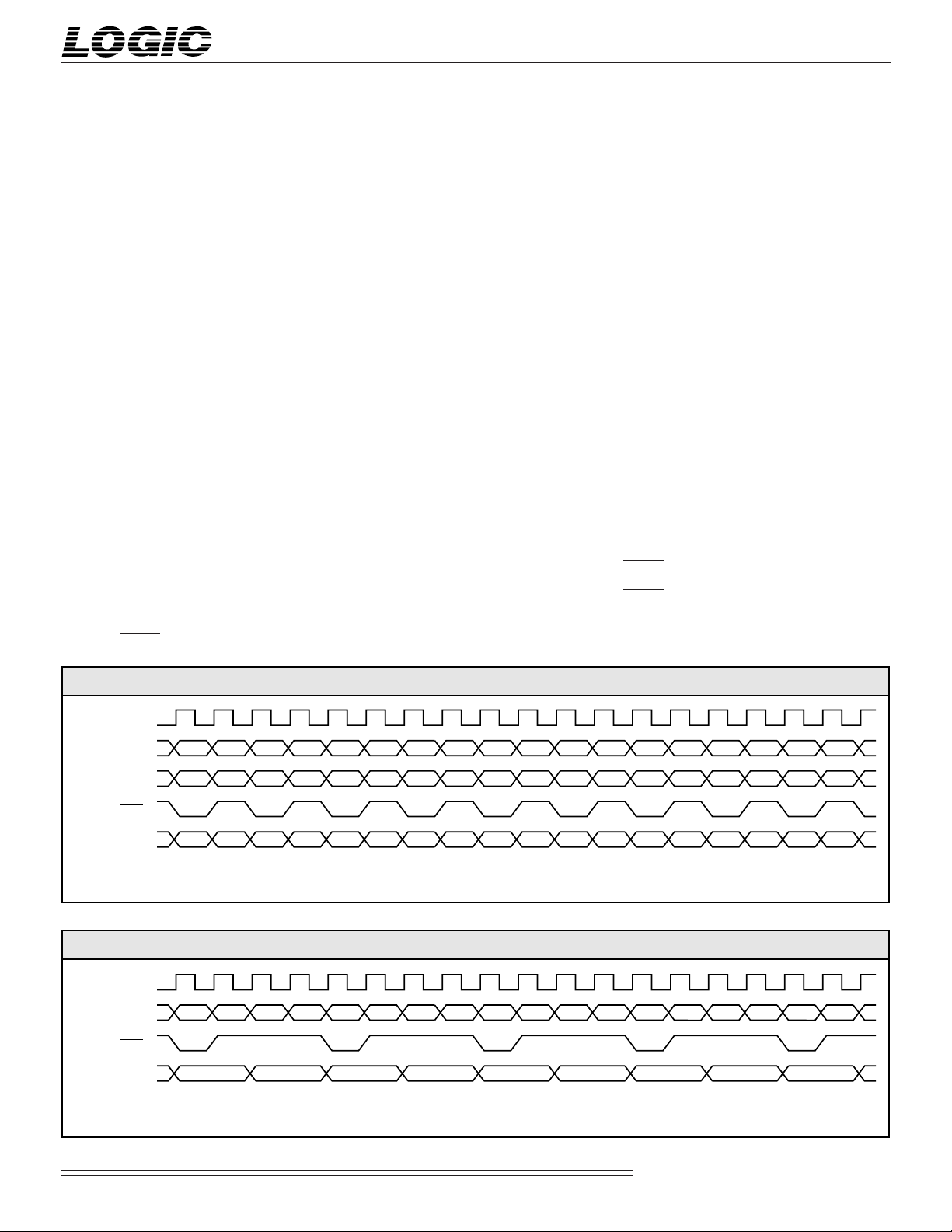
Output Multiplexer
The output multiplexer section can be
configured in various ways to accommodate the video system. Bits 2 and 3 of
Configuration Register 0 determines the
number of output channels that the
LF3370 will drive. Z12-0 is the Key
channel output port; the Key channel
simply gets passed through the output
multiplexer with a latency that matches
the other three channels.
If three separate output channels of noninterleaved video are desired, no multiplexing is performed. The three channels
are passed through the output multiplexer unmodified on the output ports
W12-0, X12-0, and Y12-0 with a delay of 2
CLK cycles. For this operation, bits 2 and
3 must both be set to 1 in Configuration
Register 0 (see Table 5).
If one channel of non-interleaved video
(i.e., Luma) and one channel of inter-
leaved video (i.e., Chroma) is desired (see
Figure 6), non-interleaved video will be
driven to the output port W12-0 and
interleaved video will be driven to the
output port X12-0 with a delay of 2 CLK
cycles. For this operation, bit 2 must be set
to 0 and bit 3 must be set to 1 in Configuration Register 0 (see Table 5).
If 4:2:2 interleaved video on one port is
desired (see Figure 7), interleaved video
will be driven to the output port W12-0
with a delay of 4 CLK cycles. For this
operation, bit 2 must be set to 1 and bit 3
must be set to 0 in Configuration Register 0
(see Table 5).
All output multiplexing operations are
initiated by the latched HIGH to LOW
transitions of SYNC which synchronizes
the multiplexed output data to the LF3370
core (see SYNC discussion).
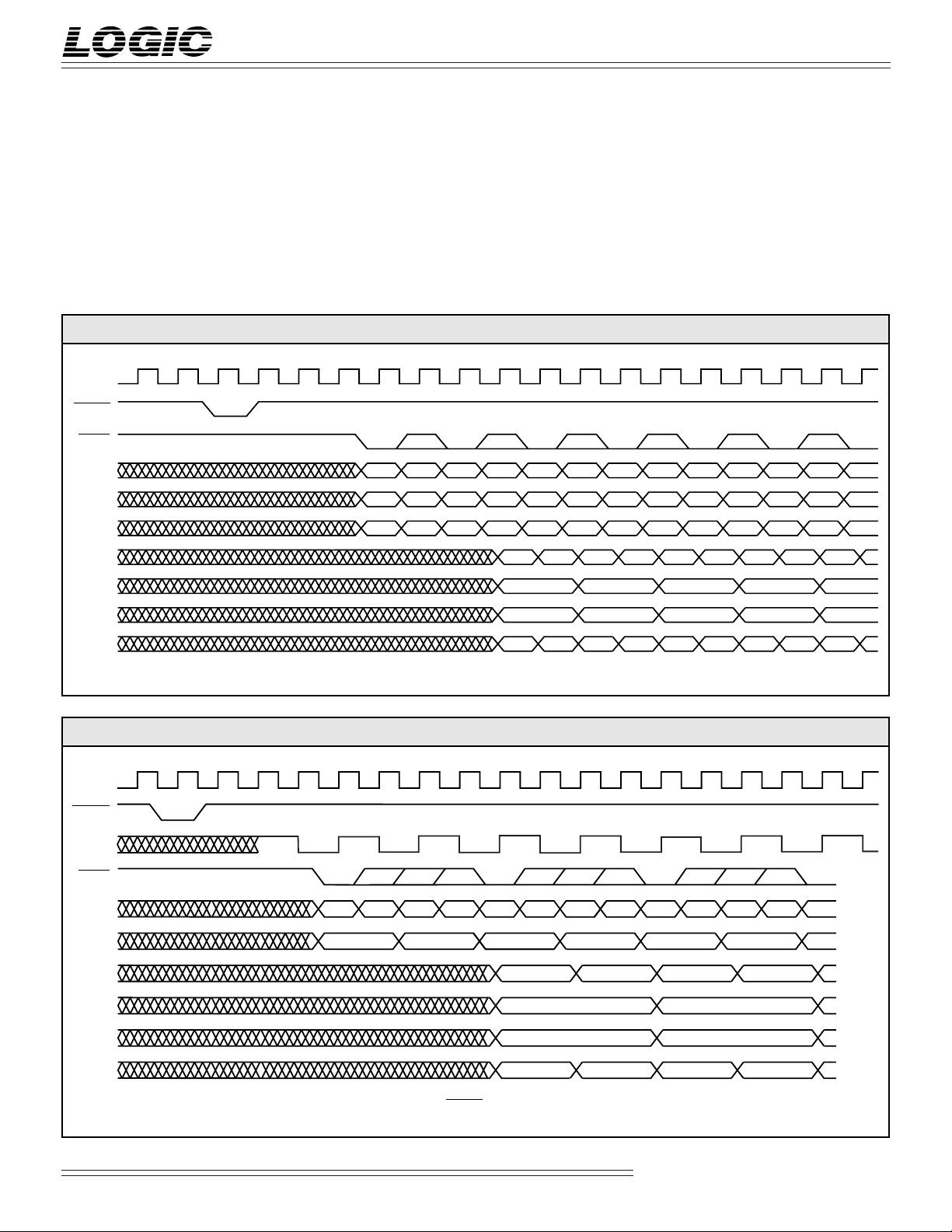
SYNC
SYNC control signal is required to
properly synchronize the input
demultiplexer, output multiplexer, and
FIGURE 6. OUTPUTTING 4:2:2:4 (INTERLEAVED CHROMA ON CHANNEL X)
CLK
Y1Y
2
Y
W
Y
0 (Output SYNC)*
12-0
X
12-0
Z
12-0
Y
0
CR0CB2CR
CB
0
K1K
K
0
There will be a HIGH to LOW transition on every Cb sample
*
3
Y
4
2
CB
2
K
3
K
4
Y
5
4
CR
4
K
5
Y
CB
K
6
6
6
Y
7
CR6CB
K
7
Y
8
Y
9
Y
10
8
CR
8
CB
10
K
8
K
9
K
10
FIGURE 7. OUTPUTTING 4:2:2:4 (INTERLEAVED LUMA/CHROMA ON CHANNEL W)
CLK
W
Y
0 (Output SYNC)*
12-0
Z
12-0
*
There will be a HIGH to LOW transition on every Cb sample
CB
0
K
Y0CR0Y
0
1
CB
2
Y
2
K
1
K
2
CR
2
Y3CB
K
3
4
Y
4
CR
4
K
K
4
5
CR
Y
Y
K
12
11
10
11
Y
5
CB
K
CB
Y
13
Y
14
12
CR
12
CB
14
12
K
13
K
14
6
Y
6
CR
6
K
K
6
7
CR
Y
16
Y
Y
15
CB
14
K
15
CR
Y
7
17
16
CR
16
K
16
K
17
8
Y
8
K
8
Video Imaging Products
7
03/13/2001–LDS.3370-F
Page 8
DEVICES INCORPORATED
LF3370
High-Definition Video Format Converter
halfband filters to the data flowing
through the LF3370. A latched HIGH to
LOW transition on SYNC control signal is
needed to initialize the device to mark the
beginning of valid data.
In addition, if 4:2:2 interleaved video data
is desired for input or output, a HIGH to
LOW transition on SYNC must be
registered by a simultaneous rising edge of
CLK and CLK/2. CLK/2 is an internal
clock that must be synchronized to CLK
by use of RESET only if the core is running
at half the rate of CLK (see RESET
discussio n and Figures 4 & 5).
Furthermore, SYNC is used to identify one
interleaved data set from another. For
example, in the case of interleaved
Chroma, Cb and Cr samples must be
properly demultiplexed and synchronized for processing.
To differentiate a Cb sample from Cr, there
needs to be a HIGH to LOW transition on
SYNC on the first Cb sample (see Figure 4
& 5); SYNC can also be toggled on every
Cb sample for re-synchronization.
In the case that Cb is the first valid data
word, SYNC may be used only once in
device initialization and kept low until re-
synchronization is desired. Therefore,
when there is a HIGH to LOW transition
on SYNC, the following is assumed: Cb
will occur on the first LOW on SYNC that
is latched, Cb will occur every two clock
cycles if interleaved Chroma is presented
to the input port B12-0, Cb will occur every
4 clock cycles if single channel 4:2:2
interleaved video is presented to the input
port A12-0.
SYNC control signal is also used to
synchronize the interpolation/decimation
output data from the Half-Band Filter to
the Output Multiplexer. This synchronization is done automatically.
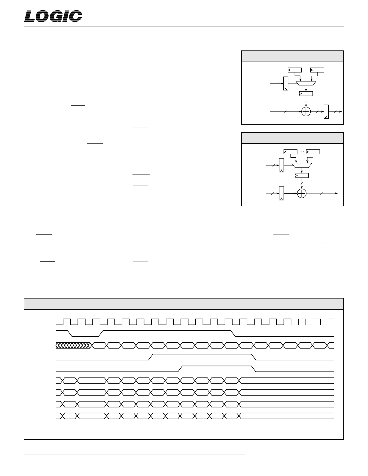
RESET
RESET should be used when initializing
the device for proper operation. It is used
to synchronize the LF3370 core clock to
the master clock. In the case that single
channel 4:2:2 interleaved video data is
desired either on the input or output, thus
using only one input or one output port
(not including Key data), the internal
clock rate will be half (CLK/2) of the
master clock rate (CLK). In this case,
RESET is needed to synchronize the rising
edge of CLK/2 to a known rising edge of
CLK (see Figure 4). For example, after
configuring the LF3370 and before
FIGURE 8. INPUT BIAS
R0R3
INBIAS
From Input Demux
2
1-0
13
13
13
13
FIGURE 9. OUTPUT BIAS
R0R3
OUTBIAS
From Core
streaming valid data through the part, a
RESET event should be used to align the
clock edges (see Figure 4 & 5).
Furthermore, RESET will clear HF0 and
HF1. A LOW state detected on RESET on a
rising edge of clock will clear flags HF0
and HF1 on the following rising edge of
clock. Please note HBLANK should be
2
1-0
13
13
13
FIGURE 10. HBLANK AND COUNTER
CLK
HBLANK
20-bit
COUNTER
HF
HF
A'
12-0*
B'
12-0*
C'
12-0*
D'
12-0*
2
1
0
0
1
D
N
HBLANK Word A
D
N
HBLANK Word B
D
N
HBLANK Word C
D
N
HBLANK Word D
Data values at output of Input LUT section
*
In this example, HF0 Count Value is set to 3 and HF1 Count Value is set to 5
41214
3
123
D
N+3DN+4DN+5
D
N+3DN+4DN+5
D
N+3DN+4DN+5
D
N+3DN+4DN+5
6
5
4
D
N+6
D
N+6
D
N+6
D
N+6
7
5
D
N+7
D
N+7
D
N+7
D
N+7
8
6
D
N+8
D
N+8
D
N+8
D
N+8
10
911
78
D
N+9DN+10
D
N+9DN+10
D
N+9DN+10
D
N+9DN+10
9
D
N+11
D
N+11
D
N+11
D
N+11
13
0
10
15
1
23
HBLANK Word A
HBLANK Word B
HBLANK Word C
HBLANK Word D
1716 18
4
5
Video Imaging Products
8
03/13/2001–LDS.3370-F
Page 9

DEVICES INCORPORATED
LF3370
High-Definition Video Format Converter
used to clear HF0 and HF1 during normal
operation (see HBLANK discussion).
are injected on the next rising clock edge
when HBLANK is LOW. In addition,
HBLANK clears flags HF0 and HF1 and
HBLANK
resets a 20-bit incrementing counter (0 1,048,575). If a HIGH to LOW transition
HBLANK is used to replace portions of the
input data with user-defined blanking
levels. When HBLANK is LOW, blanking
level words are injected into the data
stream immediately after the Input LUT
section regardless of this section being
used or not. While HBLANK is LOW,
on HBLANK is detected on a rising edge of
clock, HF0 and HF1 are cleared and the
counter is reset on the following rising
edge of clock (see Figure 10). Key Channel
blanking may be independently enabled
or disabled using Congifuration Register 1
(see Table 6).
blanking level words are continually
injected into the datapath with userdefined blanking words. Blanking words
FIGURE 11. MATRIX MULTIPLIER AND KEY SCALER
13 26
13
13
13 26
13
Coef Bank 1
13
13
Coef Bank 0
13 26
13
13 26
13
Coef Bank 2
HF0/HF1 and Counter
HF0 and HF1 are two independent flags
that are set when the pre-programmed
HF0 or HF1 count value is equal to the 20bit incrementing counter value. For each
flag, one user-defined 20-bit count value
can be programmed. When HF0 or HF1
count value is equal to the counter value,
HF0 or HF1 is set on the next rising edge
of clock. Once the flags are set, they must
be reset if they are needed again. The
counter will increment by one at the rate
of CLK and can be reset by HBLANK.
The counter will continue to loop if not
26
26 28
26
26
20(MSB)
13
LRS
’
A
13
Coef Bank 3
13 26
13
A
13
Coef Bank 6
13
D
B
13
13
13 26
13
Coef Bank 4
13 26
13
Coef Bank 7
13 26
13
Coef Bank 9
26
13 26
13
13
Coef Bank 5
13 26
13
C
13
Coef Bank 8
26
26
26
26
28
28
26
20(MSB)
20(MSB)
20(MSB)
13
’
LRS
LRS
LRS
B
13
’
C
13
’
D
Video Imaging Products
9
03/13/2001–LDS.3370-F
Page 10

DEVICES INCORPORATED
LF3370
High-Definition Video Format Converter
reset. HF0 and HF1 count value register
loading is discussed in the LF Interface™.
Please note, using HBLANK is the
recommended way of clearing HF0 and
HF1 flags but they can be cleared by
RESET, normally performed during device
initialization. RESET will not reset the
counter.
Input/Output Bias Adder
The programmable Input/Output Bias
Adders can be used to subtract or add a
13-bit offset to the data. Input and output
data formats for the two sections are
shown in Figure 3. By using INBIAS1-0,
the user may select one of four programmed Input Bias Adder values (see
Figure 8). By using OUTBIAS1-0, the user
may select one of four programmed
Output Bias Adder values (see Figure 9).
A value of 00 on INBIAS1-0/OUTBIAS1-0
selects Input/Output Bias Adder Register
0. A value of 01 selects Input/Output
Bias Adder Register 1 and so on.
INBIAS1-0/OUTBIAS1-0 may be changed
every clock cycle if desired. If a bias is not
desired, then bits 11 & 12 of Configuration
Register 1 can be set up to independently
disable the input and output bias values.
Thus, effectively zeroing the function.
The total pipeline latency from the input
to the output for each of the two sections
is one CLK cycle. Input/Output Bias
Adder Register loading is discussed in the
LF Interface™ section.
3 x 3 Matrix Multiplier
Processing almost 550 million colors, three
simultaneous 13-bit input and output
channels are utilized to implement a 3 x 3matrix multiplication (triple dot product).
Each truncated 20-bit output is the sum of
all three input words multiplied by the
appropriate coefficients (see Figure 11).
These outputs are then fed into the RSL
circuitry (see Figure 13). Input/Output
formats are shown in Figure 3.
For each of the nine multipliers, up to four
user-defined 13-bit coefficients can be
programmed and selected by CA1-0. A
value of 00 on CA1-0 selects Coefficient Set
0 on each of the 9 coefficient banks. A
value of 01 selects Coefficient Set 1 and so
on. CA1-0 may be changed every clock
cycle if desired. Coefficient bank loading is
discussed in the LF Interface™.
The total pipeline latency from the input of
the Matrix Multiplier to the output of the
RSL Circuitry is 6 CLK cycles and new
output data is subsequently available
every clock cycle thereafter.
If matrix multiplication is not desired,
using the appropriate combination of
coefficient values while keeping in mind
bit weighting, an identity matrix may be
set up to bypass the Matrix Multiplier
section (see also First Operation Select in
the Bypass Options discussion).
Key Scaler
The Key channel is equiped with a 13 x 13bit Key Scaler (see Figure 11) producing a
truncated 20-bit output which is then fed
into the RSL circuitry (see Figure 13). Up to
four user-defined 13-bit coefficients can be
programmed and selected by CA1-0.
Input/Output formats are shown in
Figure 3.
The total pipeline latency from the input of
the Key Scaler to the output of the RSL
Circuitry is 6 CLK cycles and new output
data is subsequently available every clock
cycle thereafter. If scaling is not desired,
load and select a Key Scaler Coefficient
value of 1 (see also First Operation Select in
the Bypass Options duscussion).
Half-Band Filter
There are two internal Half-Band filters in
the LF3370. These Half-Band filters can
either interpolate, decimate, or pass
through data found on channel B and
channel C. Data on channel A and
channel D in this section pass through a
programmable 127 x 13-bit delay (see
Bypass Section). The filter section (as
show in Figure 12) is a fixed-coefficient,
linear-phase half-band (low-pass)
interpolating/decimating digital filter.
The filter in this section is a 55-tap
transversal FIR with 13-bit coefficients as
shown in Table 3. The frequency response (Figure 14) is in full compliance
with SMPTE 260M. This section can be
configured for 2:1 interpolation, 1:2
decimation, or pass-through mode by
setting bits 5-8 in Configuration Register 0
(see Table 5). This section can also be
placed before or after the matrix multi-
FIGURE 12. 1:2 INTERPOLATION / 2:1 DECIMATION HALF-BAND FILTERS
VARIABLE LENGTH BYPASS DELAY
127 x 13-Bit
13
13
B
13
C
INTERPOLATION
CIRCUIT
INTERPOLATION
CIRCUIT
VARIABLE LENGTH BYPASS DELAY
55-TAP
FIR
FILTER
CONFIGURATION / CONTROL
REGISTERS
55-TAP
FIR
FILTER
127 x 13-Bit
DECIMATION
CIRCUIT
DECIMATION
CIRCUIT
LRS
LRS
13
B'
C'
Video Imaging Products
10
03/13/2001–LDS.3370-F
Page 11

DEVICES INCORPORATED
LF3370
High-Definition Video Format Converter
FIGURE 13. RSL CIRCUITRY
UL0UL3
LIMIT
LL0LL3R0R3
13
13
RSL
From Core
S0S3
2
1-0
20 13 13
20
20 13
ROUND
SELECT
TABLE 2. SELECT FORMATS
SLCT1-0 S12 S11 S10 S9 S8 S7 S6 S5 S4 S3 S2 S1 S0
00 F16 F15 F14 F13 F12 F11 F10 F9 F8 F7 F6 F5 F4
01 F17 F16 F15 F14 F13 F12 F11 F10 F9 F8 F7 F6 F5
10 F18 F17 F16 F15 F14 F13 F12 F11 F10 F9 F8 F7 F6
11 F19 F18 F17 F16 F15 F14 F13 F12 F11 F10 F9 F8 F7
plier by setting bit 4 in Configuration
Register 0 (see Table 5). The maximum
input and output clock rate this section
can operate at is the CLK rate. The total
internal pipeline latency from the input to
the output of this section (including RSL
circuitry) as shown in Figure 12 is 6 cycles.
To perform interpolation, the input data
rate of this section will be half of CLK rate.
Please note the maximum output data
rate is the CLK rate. To perform decimation, the output data rate of this section
will be half of the input data rate. One
output sample is obtained for every two
input samples.
Once an impulse is clocked into the HalfBand Filter section, the 55-value output
response begins after 8 clock cycles and
ends after 62 clock cycles. The pipeline
latency from the input of an impulse to its
corresponding output peak is 35 clock
cycles.
The input/output formats are always in
two’s complement format as shown in
Figure 3. In Interpolate Mode, the gain of
the Half-Band Filter is halved (due to half
of the input samples being padded with
zeros). A right shifted Select window is
required to maintain an overall filter gain
of 1. It is possible that ringing on the
filter’s output could cause the high order
bit (bit F18 in Figure 3 - Interpolate Filter
Output Bit Weighting) to become HIGH. If
a right shifted Select window is used, this
F18 bit becomes the sign bit of the Selected
window – and the output is erroneously
considered negative. To ensure that no
overflow conditions occur, an internal
Limiter within each Half-Band Filter
monitors its output. During Interpolate
mode, this Limiter clamps the output word
to 3FFFFH (20-bit maximum positive value
) 2) or C0000H (20-bit maximum negative
value ) 2) if a positive or negative overflow
occurs respectively. The internal 24-bits of
the Half-Band Filter are truncated to 20bits and then passed to the Round section
of the RSL circuitry; see RSL section for
further details. This section is fully
bypassable by use of programmable
delays (see Bypass Options section for
further details).
FIGURE 14. FREQUENCY RESPONSE OF FILTER
0
–10
–20
–30
–40
–50
GAIN (dB)
–60
–70
–80
0 0.1
ƒ
0.2
S
ƒ
0.3
S
ƒ
S
FREQUENCY (NORMALIZED)
0.4
Look-Up Table
Three optional programmable Input/
Output 1K x 13-bit LUTs have been
provided for Channels A, B, and C for
various uses such as Gamma Correction.
There are NOT actually two LUTs per
channel as shown in Figures 1 and 2; only
one LUT per channel can be selected for
use at any given time. The latency
through a LUT section is 2 cycles. This
latency is present on the datapath regardless of whether the LUT is in use or not.
When using a LUT, the appropriate
ƒ
0.5
S
ƒ
S
addressed value will be passed as an
Video Imaging Products
11
03/13/2001–LDS.3370-F
Page 12

DEVICES INCORPORATED
LF3370
High-Definition Video Format Converter
output of the LUT section. The Gamma
LUT address can be chosen from any of
the 4 possible10-bit words that are
‘window’ selected from the13-bit Input
data bus. Configuring the desired LUT
address selector position is accomplished
by programming bits 10 & 9 of Configuration Register 1. Once the LUT Select Data
position is programmed, it is meant to
control all three Gamma LUTs. Therefore,
the address selector positions of the three
LUTs cannot be independently controlled.
LUT loading is discussed in the LF
Interface™ section.
Rounding
The rounding circuitry found in the Matrix
Multiplier and Half-Band Filter sections
work in the same manner. The truncated
20 MSBs from the Matrix Multiplier or
Half-Band Filter output may be rounded
by being added to the contents of one of the
four Round Registers (see Figure 13). Each
round register is 20 bits wide and userprogrammable. This allows the Matrix
Multiplier’s or Half-Band Filter’s output to
be rounded to any precision required.
RSL1-0 determines which of the four
Round Registers are used in each Rounding Circuitry. A value of 00 on RSL1-0
selects Round Register 0. A value of 01
selects Round Register 1 and so on. RSL1-
0 may be changed every clock cycle if
desired. If rounding is not desired, the
user must load and select a Round
Register with value of 0. Round Register
loading is discussed in the LF Interface™
section.
Selecting
The selecting circuitry found in the Matrix
Multiplier and Half-Band Filter sections
work in the same manner. The output
word of the Matrix Multiplier and HalfBand Filter feeding the RSL circuitry is the
20 MSBs. However, only 13 bits may be
sent to the next section. Therefore, the
Select Register determines which 13-bits
are passed. There are four select registers;
RSL1-0 determines which of the four Select
Registers are used in each Select Circuitry
(see Table 2). A value of 00 on RSL1-0
selects Select Register 0. A value of 01
selects Select Register 1 and so on. RSL1-0
may be changed every clock cycle if
desired. This allows the 13-bit window to
be changed every clock cycle. Select
Register loading is discussed in the
LF Interface™ section.
Limiting
The Limiting Circuitry found in the Matrix
Multiplier and Half-Band Filter sections
work in the same manner. The Limit
Registers determine the valid range of
output values for each of these two
sections. There are four 13-bit Limit
the Limiting Circuitry is less than the
lower limit, the lower limit value is passed
as the Matrix Multiplier section’s or HalfBand filter section’s output. If the value
fed to the Limiting Circuitry is greater
than the upper limit, the upper limit value
is passed as the Matrix Multiplier section’s
or Half-Band filter section’s output.
RSL1-0 may be changed every clock cycle if
desired thus allowing the limit range to be
changed every clock cycle. When loading
limit values into the device, the upper limit
must be greater than the lower limit. The
most negative and most positive values
you can load into the Limit Registers are
0FFFH and 1000H. Limit Register loading
is discussed in the LF Interface™ section.
Registers for each section. RSL1-0 determines which of the four Limit Registers
are used in each Limiting Circuitry (see
Figure 13). A value of 00 on RSL1-0 selects
Limit Register 0. A value of 01 selects
Limit Register 1 and so on.
Each Limit Register contains an upper
and lower limit value. If the value fed to
LF Interface™
The LF Interface™ is used to load the
Configuration Registers, Matrix Multiplier/Key Scaler Coefficient Banks, LookUp Tables, Input/Output Bias registers,
RSL registers, HF0 and HF1 Count Values,
and Horizontal Blanking Levels.
TABLE 3. HALF-BAND FILTER IMPULSE RESPONSE
Impulse Response Out (Non-Interpolated Bit Weighing)
TAP 20-bit (MSB) Filter Out (HEX) Decimal Equivalent
1, 55 FFE35 –0.0008755
2, 54 0 0
3, 53 002D2 0.0013771
4, 52 0 0
5, 51 FFB5C –0.00226593
6, 50 0 0
7, 49 00725 0.0034885
8, 48 0 0
9, 47 FF508 –0.0053558
10, 46 0 0
11, 45 00F95 0.0076084
12, 44 0 0
13, 43 FEA10 –0.01071167
14, 42 0 0
15, 41 01E59 0.0148182
16, 40 0 0
17, 39 FD6A8 –0.02018738
18, 38 0 0
19, 37 0393E 0.0279503
20, 36 0 0
21, 35 FAF1B –0.0394993
22, 34 0 0
23, 33 0798D 0.05935097
24, 32 0 0
25, 31 F2BD2 –0.10360334
26, 30 0 0
27, 29 28B30 0.3179626
28 (center) 401BC 0.500846862
Video Imaging Products
12
03/13/2001–LDS.3370-F
Page 13

DEVICES INCORPORATED
FIGURE 15. BYPASS BLOCK DIAGRAM
LF3370
High-Definition Video Format Converter
A,
B,
C,
D
INPUT
DEMUX
SECTION
In this example, the Matrix-Multipler/Key Scaler Section feeds the Half-Band Filter Section. This arrangement is reversible.
INPUT
BIAS
SECTION
FIGURE 16. CORE BYPASS
CLK
DATAPASS
Core Data
Bypass Data
Output*
In this example, the Output Multiplexer is in a mode where the delay through the section is 2 CLK cycles. Only one channel is shown in this example,
*
however, the other three channels behave in the same manner. The example assumes that the bypass RAM length is set to the length of the core data path.
W1: Bypass data is output to the output port and replaces core data.
W2: Core data is output to the output port and replaces bypass data.
D
0
B
0
D1D2D
B
1
B
2
D0D
LUT
SECTION
MATRIX MULTIPLIER
3
D
B
3
B
1
D
and KEY SCALER
SECTION
4
D
5
4
B
5
2
D
3
13
13
D
6
B
6
D
4
VARIABLE LENGTH
BYPASS DELAY
(127 x 13-Bit )
VARIABLE LENGTH
BYPASS DELAY
(127 x 13-Bit )
HALF-BAND
FILTER
SECTION
W1 W2
D7D
B
D5B
8
D
9
D
7
B
8
B
9
B
6
B
7
B
13
13
LUT
SECTION
D
D
10
B
10
8
12
11
B
12
11
B
10
B
9
OUTPUT
BIAS
SECTION
D
13
D
14
B
13
B
14
B
11
B
12
OUTPUT
MUX
SECTION
D
D
B
D
16
15
B
16
15
D
14
13
W,
X,
Y,
Z
D
17
B
17
D
15
TABLE 4. CONFIGURATION/CONTROL REGISTERS ADDRESSING SUMMARY
DESCRIPTION ADDRESS RANGE (HEX)
Coefficient Registers 0000 - 0003
Configuration Registers 0200 - 020A
Look-Up Table - Channel ‘A’ 0300
Look-Up Table - Channel ‘B’ 0400
Look-Up Table - Channel ‘C’ 0500
Input Bias Registers - Channel ‘A’ 0600 - 0603
Input Bias Registers - Channel ‘B’ 0700 - 0703
Input Bias Registers - Channel ‘C’ 0800 - 0803
Output Bias Registers - Channel ‘A’ 0900 - 0903
Output Bias Registers - Channel ‘B’ 0A00 - 0A03
Output Bias Registers - Channel ‘C’ 0B00 - 0B03
HF0 Count Value 0C00
HF1 Count Value 0D00
Matrix Mult. RSL Registers - Channel ‘A’ 0E00 - 0E03
Matrix Mult. RSL Registers - Channel ‘B’ 0F00 - 0F03
Matrix Mult. RSL Registers - Channel ‘C’ 1000 - 1003
Key Scaler RSL Registers 1100 - 1103
Half-Band Filter RSL Registers - Channel ‘B’ 1200 - 1203
Half-Band Filter RSL Registers - Channel ‘C’ 1300 - 1303
LD is used to enable and disable the
LF Interface™. When LD goes LOW, the
LF Interface™ is enabled for data input.
The first value fed into the interface on
CF12-0 is an address which determines
what the interface is going to load (see
Table 4). For example, to load address
Bias Adder Register 2 of the channel B
Output Bias Adder, the first data value
into the LF Interface™ should be 0A02H.
To load RSL Register 1 for the Keyscaler
RSL, the first data value should be 1101H.
The first address value should be loaded
into the interface on the same clock cycle
that latches the HIGH to LOW transition
of LD. The next value(s) loaded into the
interface are the data value(s) which will
be stored in the bank or register defined
by the address value. When loading
coefficient banks, the interface will expect
ten values to be loaded into the device
after the address value. The ten values are
coefficients 0 through 8 and the Keyscale
coefficient. When loading Configuration
or Bias Registers, the interface will expect
one value after the address value. When
loading RSL registers, the interface will
Video Imaging Products
13
03/13/2001–LDS.3370-F
Page 14

DEVICES INCORPORATED
LF3370
High-Definition Video Format Converter
expect four values after the address value.
When loading gamma look-up tables, the
interface will expect 1024 values after the
address value. When loading HBLANK
flag counts, the interface will expect 2
values after the address value.
The coefficient banks, configuration
registers, RSL registers, etc., are not loaded
with data until all data values for the
specified address are loaded into the LF
Interface. In other words, the coefficient
banks are not written until all ten coefficients have been loaded into the LF
Interface™. A RSL register is not written to
until all four data words are loaded. After
the last data value is loaded, the interface
will expect a new address value on the
next clock cycle. After the next address
value is loaded, data loading will begin
again as previously discussed.
PAUSE allows the user to effectively slow
the rate of data loading through the
LF Interface™. When PAUSE is HIGH,
the LF Interface™ is held until PAUSE is
returned LOW. Figure 19 shows the
effects of PAUSE while loading Matrix
Multiplier/Key Scaler coefficients.
Table 28 shows an example of loading a
bias value into the Input Bias Adder
Register. In this example, a bias value of
007FH is loaded into the Channel ‘C’
Input Bias Adder Register 1 (0B01H).
Table 29 shows an example of loading a
bias value into the Output Bias Adder
Register. In this example, a bias value of
0010H is loaded into Channel ‘A’ Output
Bias Adder Register 3 (0903H).
Table 30 shows an example of loading
data into the Matrix Multiplier/Key
Scaler Coefficient Banks. In this example,
the following values are loaded into
Coefficient Register Set 2 (0002H): 0000H,
0001H, 0002H, 0003H, 0004H, 0005H,
0006H, 0007H, 0008H, and 0009H.
Table 31 shows an example of loading the
HF0 Flag Count Value. In this example, a
20-bit HF0 Flag Count Value of B3C27H is
loaded into the HF0 Flag Count Value
TABLE 5. CONFIGURATION REGISTER 0 – ADDRESS 200H
BITS FUNCTION DESCRIPTION
1-0 Video Input Format 00 : Reserved
01 : Single Channel Interleaved Video
10 : Dual Channel Interleaved Video
11 : 3 Channel Non-Interleaved Video
3-2 Video Output Format 00 : Reserved
4 Functional Arrangement 0 : Filter Feeds Matrix Multiplier
6-5 Half-Band Filter Control 00 : Pass Through Filter
Channel ‘B’ 01 : Interpolate
8-7 Half-Band Filter Control 00 : Pass Through Filter
Channel ‘C’ 01 : Interpolate
9 First Operation Select 0 : Normal Order of Operations
12-10 Reserved Must be Set to Zero
01 : Single Channel Interleaved Video
10 : Dual Channel Interleaved Video
11 : 3 Channel Non-Interleaved Video
1 : Matrix Multiplier Feeds Filter
10 : Decimate
11 : Bypass Filter
10 : Decimate
11 : Bypass Filter
1 : Select First Operation Only
TABLE 6. CONFIGURATION REGISTER 1 – ADDRESS 201H
BITS FUNCTION DESCRIPTION
1-0 Look-Up Table Control 00 : Disable Look-Up Table
3-2 Look-Up Table Control 00 : Disable Look-Up Table
5-4 Look-Up Table Control 00 : Disable Look-Up Table
6 HBLANK Control 0 : Disable Horizontal Blanking Option
8-7 Data Bypass Mode ‘W’ 00 : Output Channel ‘A’ to W
10-9 Look-Up Table Input 00 : Select Address Data [9:0]
11 Input Bias Disable 0 : Enable Input Bias
12 Output Bias Disable 0 : Enable Output Bias
Channel ‘A’ 01 : Enable Look-Up Table on Input
10 : Enable Look-Up Table on Output
11 : Reserved
Channel ‘B’ 01 : Enable Look-Up Table on Input
10 : Enable Look-Up Table on Output
11 : Reserved
Channel ‘C’ 01 : Enable Look-Up Table on Input
10 : Enable Look-Up Table on Output
11 : Reserved
‘Key’ Channel During HBLANK Period
1 : Enable Horizontal Blanking Option
During HBLANK Period
12-0
Output Channel Mux Control 01 : Output Channel ‘B’ to W12-0
10 : Output Channel ‘C’ to W12-0
11 : Output Channel ‘D’ to W12-0
Address Selection Control 01 : Sele ct Address Data [10:1]
10 : Select Address Data [11:2]
11 : Select Address Data [12:3]
1 : Disable Input Bias
1 : Disable Output Bias
Video Imaging Products
14
03/13/2001–LDS.3370-F
Page 15

DEVICES INCORPORATED
LF3370
High-Definition Video Format Converter
Register (0C00H). The HF1 Flag Count
Value is loaded in the same manner using
the appropriate address.
Table 32 shows an example of loading
Round/Select/Limit values. In this
example, Channel ‘A’ Matrix Multiplier
Register Set 0 (0E00H) is loaded with a 20bit Round value of 00020H, a 2-bit Select
value of 10H, a 13-bit Upper Limit value of
0FFFH, and a 13-bit Lower Limit value of
1001H. Other RSL registers are loaded in
the same manner using the appropriate
address.
Table 33 shows an example of loading a
Configuration Register. In this example,
Configuration Register 0 (0200H) is
loaded with 00AEH. This will setup the
Input Section to handle Luma on input
port A12-0 and interleaved Chroma on the
input port B12-0. The Output Section is
setup to output RGB on the output ports
W12-0, X12-0, Y12-0. The ‘functional
arrangement’ is setup in such a way that
the Half-Band Filter section is placed
before the Matrix Multiplier section. The
Half-Band Filters are setup for 1:2
interpolation and ‘normal order of
operations’ is selected.
Scaler Section, and Output Bias and feeds
the Output Multiplexer. Loading
Configuration Register 2 programs the
length of all four Core Bypass Delays (see
Table 7).
A LOW state detected on DATAPASS on
a rising edge of clock will output bypassed data to the output port on the
following rising edge of CLK (see Figure
X). In addition, any of the four bypassed
channels can be passed to the ‘W’ output
channel during a ‘bypass’ event. For this
operation, use bits 7 and 8 of Configuration Register 1 (see Table 6).
Half-Band Filter Bypass
At all times, while data is being fed into the
Half-Band Filter section, channels A, B, C,
and Key are fed into programmable length
delays. When the Half-Band Filter(s) are
set to filter bypass mode, that particular
channel passes through a programmable
delay and is not filtered. Since there are
only two Half-Band Filters in this section
found on channels B and C, channels A
and Key are always passed through their
respective programmable delays.
Please note, when using a single channel
video input or video output (interleaved
4:2:2), the Core Bypass Delay must be
TABLE 7. CONFIGURATION REGISTER 2 – ADDRESS 202H
BITS FUNCTION DESCRIPTION
6-0 Core Bypass Delay Length Length of Core Bypass Delay Minus 2
12-7 Reserved Must be Set to Zero
TABLE 8. CONFIGURATION REGISTER 3 – ADDRESS 203H
BITS FUNCTION DESCRIPTION
6-0 Channel ‘A’ Filter Section Length of Filter Bypass Delay Minus 2
Bypass Delay Length
12-7 Reserved Must be Set to Zero
BYPASS OPTIONS
Core Bypass
At all times during the normal operation
of the LF3370, video data on channels A,
B, C, and D are simultaneously being fed
from the output of the Input
Demultiplexer into the programmable
Core Bypass Delay (see Figure 15). This
allows users to switch between processed
video and unprocessed (bypassed) data
on-the-fly.
There is a separate Core Bypass Delay for
each channel. Each Core Bypass Delay
can be programmed for a length of 2 up to
129 CLK cycles for delay matching
between the bypass path and the core as
well as other operations. The Core Bypass
Delay bypasses the Input Bias, Input LUT,
Half-Band Filter, Matrix Multiplier/Key
TABLE 9. CONFIGURATION REGISTER 4 – ADDRESS 204H
BITS FUNCTION DESCRIPTION
6-0 Channel ‘B’ Filter Section Length of Filter Bypass Delay Minus 2
Bypass Delay Length
12-7 Reserved Must be Set to Zero
TABLE 10. CONFIGURATION REGISTER 5 – ADDRESS 205H
BITS FUNCTION DESCRIPTION
6-0 Channel ‘C’ Filter Section Length of Filter Bypass Delay Minus 2
Bypass Delay Length
12-7 Reserved Must be Set to Zero
TABLE 11. CONFIGURATION REGISTER 6 – ADDRESS 206H
BITS FUNCTION DESCRIPTION
6-0 Key Channel Filter Section Length of Filter Bypass Delay Minus 2
Bypass Delay Length
12-7 Reserved Must be Set to Zero
Video Imaging Products
15
03/13/2001–LDS.3370-F
Page 16

DEVICES INCORPORATED
LF3370
High-Definition Video Format Converter
TABLE 12. CONFIGURATION REGISTER 12 – ADDRESS 207
BITS FUNCTION DESCRIPTION
12-0 Channel ‘A’ Blanking Word Channel ‘A’ Blanking Level Word
TABLE 13. CONFIGURATION REGISTER 13– ADDRESS 208
BITS FUNCTION DESCRIPTION
12-0 Channel ‘B’ Blanking Word Channel ‘B’ Blanking Level Word
TABLE 14. CONFIGURATION REGISTER 14 – ADDRESS 209
BITS FUNCTION DESCRIPTION
12-0 Channel ‘C’ Blanking Word Channel ‘C’ Blanking Level Word
TABLE 15. CONFIGURATION REGISTER 15 – ADDRESS 20A
BITS FUNCTION DESCRIPTION
12-0 Channel ‘D’ Blanking Word Channel ‘D’ Blanking Level Word
programmed to double the length [(desired length x 2) – 2)] to properly align
data due to the core running at half the
CLK rate.
First Operation Select
‘First Operation Select’ is a bypassing
option where you select to use the first
functional block (Half-Band Filter or
Matrix Multiplier/Key Scaler) in any given
arrangement. If the device was arranged in
such a way that the Half-Band Filter section
fed the Matrix Multiplier/Key Scaler section
and ‘First Operation Select’ was enabled,
the Half-Band Filter section will be used
and the Matrix Multiplier/Key Scaler
section will be bypassed.
If the device was arranged in such a way
that the Matrix Multiplier/Key Scaler
section fed the Half-Band Filter section
and ‘First Operation Select’ was enabled,
the Matrix Multiplier/Key Scaler section
will be used - its output will be routed
directly to the output LUT section. Unlike
in other bypassing options , the total
pipeline latency of the LF3370 is reduced
by the appropriate delay. If the Half-Band
Filter section was bypassed by this method,
the overall pipeline latency should be
reduced by 35 CLK cycles. If the Matrix
Multiplier section was bypassed by this
method, the overall pipeline latency
should be reduced by 6 CLK cycles. This
function is implemented by configuring bit
9 of Configuration Register 0. The ‘Functional Arrangement’ of the device is
determined by configuring bit 4 of Configuration Register 0.
Video Imaging Products
16
03/13/2001–LDS.3370-F
Page 17

DEVICES INCORPORATED
LF3370
High-Definition Video Format Converter
TABLE 16. CHANNEL ‘A’ INPUT
BIAS REGISTERS
REGISTER ADDRESS (HEX)
0 0600
1 0601
2 0602
3 0603
TABLE 19. CHANNEL ‘A’ OUTPUT
BIAS REGISTERS
REGISTER ADDRESS (HEX)
0 0900
1 0901
2 0902
3 0903
TABLE 22. CHANNEL ‘A’ MATRIX
MULT. RSL REGISTERS
REGISTER ADDRESS (HEX)
0 0E00
1 0E01
2 0E02
3 0E03
TABLE 17. CHANNEL ‘B’ INPUT
BIAS REGISTERS
REGISTER ADDRESS (HEX)
0 0700
1 0701
2 0702
3 0703
TABLE 20. CHANNEL ‘B’ OUTPUT
BIAS REGISTERS
REGISTER ADDRESS (HEX)
0 0A00
1 0A01
2 0A02
3 0A03
TABLE 23. CHANNEL ‘B’ MATRIX
MULT. RSL REGISTERS
REGISTER ADDRESS (HEX)
0 0F00
1 0F01
2 0F02
3 0F03
TABLE 18. CHANNEL ‘C’ INPUT
BIAS REGISTERS
REGISTER ADDRESS (HEX)
0 0800
1 0801
2 0802
3 0803
TABLE 21. CHANNEL ‘C’ OUTPUT
BIAS REGISTERS
REGISTER ADDRESS (HEX)
0 0B00
1 0B01
2 0B02
3 0B03
TABLE 24. CHANNEL ‘C’ MATRIX
MULT. RSL REGISTERS
REGISTER ADDRESS (HEX)
0 1000
1 1001
2 1002
3 1003
TABLE 25. ‘K EY’ CHANNEL MATRIX
MULT. RSL REGISTERS
REGISTER ADDRESS (HEX)
0 1100
1 1101
2 1102
3 1103
TABLE 28 HF X COUNT VALUE REGISTERS
COUNT ADDRESS (HEX)
0 0C00
1 0D00
T ABLE 31.LOOK-UP TABLE ADDRESSING
CHANNEL ADDRESS (HEX)
‘A’ 0300
‘B’ 0400
‘C’ 0500
TABLE 26. CHANNEL ‘B’ HALFBAND
FILTER RSL REGISTERS
REGISTER ADDRESS (HEX)
0 1200
1 1201
2 1202
3 1203
TABLE 29. HORIZONTAL BLANKING
LEVEL ADDRESS
CHANNEL ADDRESS (HEX)
‘A’ 0207
‘B’ 0208
‘C’ 0209
‘D’ 020A
TABLE 27. CHANNEL ‘C’ HALFBAND
FILTER RSL REGISTERS
REGISTER ADDRESS (HEX)
0 1300
1 1301
2 1302
3 1303
TABLE 30. MATRIX MULT. & SCALER
COEFFICIENT REGISTERS
REGISTER ADDRESS (HEX)
0 0000
1 0001
2 0002
3 0003
Video Imaging Products
17
03/13/2001–LDS.3370-F
Page 18

LF3370
DEVICES INCORPORATED
TABLE 32. INTPUT BIAS ADDER REGISTER LOADING FORMAT
CF12 CF11 CF10 CF9 CF8 CF7 CF6 CF5 CF4 CF3 CF2 CF1 CF0
Address 0101100000001
Word 0 0000001111111
TABLE 33. OUTPUT BIAS ADDER REGISTER LOADING FORMAT
CF12 CF11 CF10 CF9 CF8 CF7 CF6 CF5 CF4 CF3 CF2 CF1 CF0
Address 0100100000011
Word 0 0000000010000
TABLE 34 MATRIX MULTIPLIER/KEY SCALER COEFFICIENT BANK LOADING FORMAT
CF12 CF11 CF10 CF9 CF8 CF7 CF6 CF5 CF4 CF3 CF2 CF1 CF0
Address 0000000000010
Coef Bank 0 0000000000000
Coef Bank 1 0000000000001
Coef Bank 2 0000000000010
High-Definition Video Format Converter
Coef Bank 3 0000000000011
Coef Bank 4 0000000000100
Coef Bank 5 0000000000101
Coef Bank 6 0000000000110
Coef Bank 7 0000000000111
Coef Bank 8 0000000001000
Coef Bank 9 0000000001001
TABLE 35. HFX COUNT VALUE LOADING FORMAT
CF12 CF11 CF10 CF9 CF8 CF7 CF6 CF5 CF4 CF3 CF2 CF1 CF0
Address 0110000000000
Word 0 R110000100111
Word 1 RRRRR10110011
HF19
HF0
TABLE 36. RSL REGISTER LOADING FORMAT
CF12 CF11 CF10 CF9 CF8 CF7 CF6 CF5 CF4 CF3 CF2 CF1 CF0
Address 0111000000000
Word 0 R000000100000
Word 1 RRR0100000000
Word 2 0111111111111
Word 3 1000000000001
UL12
LL12
S1 R 19S0
R0
UL0
LL0
TABLE 37. CONFIGURATION REGISTER LOADING FORMAT
CF12 CF11 CF10 CF9 CF8 CF7 CF6 CF5 CF4 CF3 CF2 CF1 CF0
Address 0001000000000
Word 0 0000010101110
Video Imaging Products
18
03/13/2001–LDS.3370-F
Page 19

LF3370
DEVICES INCORPORATED
FIGURE 17.C ONFIGURATION, INPUT/OUTPUT BIAS ADDER, RSL, AND HBLANK LEVEL REGISTER LOADING SEQUENCE
High-Definition Video Format Converter
CONFIG REG RSL REGISTER
IN/OUT BIAS REG
CLK
W1
LD
CF
12-0
ADDR1DATA
1
ADDR
DATA
1
ADDR
2
W1: Configuration Register updated and effective on this rising clock edge.
W2: Input or Output Bias Adder Register updated and effective on this rising clock edge.
W3: RSL Register Set updated and effective on this rising clock edge.
W4: Horizontal Blanking Level Register updated and effective on this rising clock edge.
FIGURE 18.LOOK-U P TABLE LOADING SEQUENCE
CLK
LD
CF
11-0
ADDR1N
W1: LUT updated and effective on this rising clock edge.
N
1
0
N
N
3
2
HBLANK LEVEL REGISTER
W2
3
1
DATA
DATA
2
DATA
DATA
4
3
ADDR
4
DATA
W3 W4
DATA
1
2
W1
N
4
N
1019
1020
N
1021
N
1022
N
1023
N
FIGURE 19.MATRIX MULTIPLIER/KEY SCALER COEFFICIENT BANK LOADING SEQUENCE
CLK
W1
LD
CF
12-0
ADDR1COEF
0
COEF2COEF3COEF
COEF
1
4
COEF6ADDR7COEF
COEF
5
8
COEF
9
W1: Matrix Multiplier/Key Scaler Coefficient Set updated and effective on this active rising clock edge.
FIGURE 20.MATRIX MULTIPLIER/KEY SCALER COEFFICIENT BANK LOADING SEQUENCE WITH PAUSE IMPLEMENTATION
CLK
W1
PAUSE
LD
ADDR
12-0
CF
W1: Matrix Multiplier/Key Scaler Coefficient Set updated and effective on this active rising clock edge.
1
COEF
0
COEF
1
COEF
9
Video Imaging Products
19
03/13/2001–LDS.3370-F
Page 20

DEVICES INCORPORATED
LF3370
High-Definition Video Format Converter
MAXIMUM RATINGS
Storage temperature ............................................................................................................. –65°C to +150°C
Operating ambient temperature................................................................................................... 0°C to +70°C
VCC supply voltage with respect to ground ............................................................................ –0.5 V to +4.5V
Input signal with respect to ground........................................................................................... –0.5 V to 5.5 V
Signal applied to high impedance output .................................................................................. –0.5 V to 5.5 V
Output current into low outputs ............................................................................................................. 25 mA
Latchup current................................................................................................................................ > 400 mA
OPERATING CONDITIONS
Active Operation, Commercial 0°C to +70°C 3.00 V ≤ VCC ≤ 3.60 V
Above which useful life may be impaired (Notes 1, 2, 8)
To meet specified electrical and switching characteristics
Mode Temperature Range (Ambient) Supply Voltage
ELECTRICAL CHARACTERISTICS
Symbol Parameter Test Condition Min Typ Max Unit
VOH Output High Voltage VCC = Min., IOH = –4 mA 2.4 V
VOL Output Low Voltage VCC = Min., IOL = 8.0 mA 0.4 V
VIH Input High Voltage 2.0 5.5 V
V IL Input Low Voltage 0.0 0.8 V
IIX Input Current Ground ≤ VIN ≤ 5.25 V (Note 12) ±10 µA
IOZ Output Leakage Current Ground ≤ VOUT ≤ 5.25 V (Note 12) ±10 µA
ICC1 VCC Current, Dynamic At Max Operating Frequency 100 mA
CIN Input Capacitance TA = 25°C, f = 1 MHz 1 0 pF
COUT Output Capacitance TA = 25°C, f = 1 MHz 10 pF
Over Operating Conditions (Note 4)
Video Imaging Products
20
03/13/2001–LDS.3370-F
Page 21

DEVICES INCORPORATED
SWITCHING CHARACTERISTICS
LF3370
High-Definition Video Format Converter
COMMERCIAL OPERATING RANGE (0°C to +70°C)
Notes 9, 10 (ns)
LF3370–
12
Symbol Parameter Min Max
tCYC Cycle Time 12
tPWL Clock Pulse Width Low 5
tPWH Clock Pulse Width High 5
tS Input Setup Time 4
tH Input Hold Time 0
tSCT Setup Time Control Inputs 4
tHCT Hold Time Control Inputs 0
tD Output Delay 8
tDIS Three-State Output Disable Delay (Note 11) 10
tENA Three-State Output Enable Delay (Note 11) 10
SWITCHING WAVEFORMS:DATA I/O
A, B, C, D
CLK
12-0
123456
t
H
t
S
A, B, C, D
N
A, B, C, D
N+1
t
PWH
t
CYC
t
PWL
7
CA
CONTROLS
(Except OE)
W, X, Y, Z
OE
12-0
1-0
t
SCT
CA
N
t
HCT
CA
N+1
t
t
DIS
HIGH IMPEDANCE
ENA
W, X, Y, ZN-
t
D
1
W, X, Y, Z
N
Video Imaging Products
21
03/13/2001–LDS.3370-F
Page 22

DEVICES INCORPORATED
LF3370
High-Definition Video Format Converter
COMMERCIAL OPERATING RANGE (0°C to +70°C)
Notes 9, 10 (ns)
LF3370–
12
Symbol Parameter Min Max
tCFS Configuration Input Setup 5.5
tCFH Configuration Input Hold 0
tLS Load Setup Time 4
tLH Load Hold Time 0
tPS PAUSE Setup Time 4
tPH PAUSE Hold Time 0
SWITCHING WAVEFORMS: LF INTERFACE
CLK
PAUSE
CF
11 0
t
LS
LD
t
CFS
12 453
t
PWL
t
CYC
CF
0
ADDRESS
t
PWH
t
CFH
TM
6
t
LH
t
PS
t
PH
CF
1
CF
2
Video Imaging Products
22
03/13/2001–LDS.3370-F
Page 23

DEVICES INCORPORATED
ORDERING INFORMATION
160-pin
GND
BIN6
BIN7
BIN8
BIN9
BIN10
BIN11
BIN12
AIN0
AIN1
AIN2
AIN3
AIN4
AIN5
AIN6
AIN7
AIN8
AIN9
AIN10
AIN11
AIN12
RSL1
RSL0
GND
CF0
CF1
CF2
CF3
CF4
CF5
CF6
CF7
CF8
CF9
CF10
CF11
CF12
PAUSE
LF3370
High-Definition Video Format Converter
BIN5
BIN4
BIN3
BIN2
BIN1
BIN0
CIN12
CIN11
CIN10
CIN9
CIN8
CIN7
CIN6
CIN5
CIN4
CIN3
CIN2
CIN1
CIN0
GND
DIN12
DIN11
DIN10
DIN9
DIN8
DIN7
DIN6
DIN5
DIN4
DIN3
DIN2
DIN1
DIN0
Vcc
CLK
GND
Vcc
GND
CA1
CA0
160
159
158
157
156
155
154
153
152
151
150
149
148
147
146
145
144
143
142
141
140
139
138
137
136
135
134
133
132
131
130
129
128
127
126
125
124
123
122
121
INBIAS1
1
2
3
4
5
6
7
8
9
10
11
12
13
14
15
16
17
18
19
20
21
Vcc
22
23
24
25
26
27
28
29
30
31
32
33
34
35
36
37
38
LD
39
40
4344454647484950515253545556575859606162636465666768697071727374757677
41
42
Top
View
120
INBIAS0
119
OUTBIAS1
118
OUTBIAS0
117
DATAPASS
116
HBLANK
115
RESET
114
SYNC
113
GND
112
ZOUT0
111
ZOUT1
110
ZOUT2
109
ZOUT3
108
ZOUT4
107
Vcc
106
GND
105
ZOUT5
104
ZOUT6
103
ZOUT7
102
ZOUT8
101
ZOUT9
100
Vcc
99
GND
98
ZOUT10
97
ZOUT11
96
ZOUT12
95
YOUT0
94
YOUT1
93
Vcc
92
GND
91
YOUT2
90
YOUT3
89
YOUT4
88
YOUT5
87
YOUT6
86
Vcc
85
YOUT7
84
YOUT8
83
YOUT9
82
YOUT10
81
78
79
80
Speed
12 ns
HF1
HF0
GND
WOUT12
WOUT11
WOUT10
WOUT9
0°C to +70°C — COMMERCIAL SCREENING
Vcc
GND
WOUT8
WOUT7
WOUT6
WOUT5
WOUT4
WOUT3
WOUT2
WOUT1
WOUT0
XOUT12
Plastic Quad Flatpack
LF3370QC12
Vcc
XOUT11
(Q6)
GND
XOUT9
XOUT10
XOUT8
XOUT7
XOUT6
XOUT5
Vcc
GND
XOUT4
XOUT3
XOUT2
XOUT1
XOUT0
OE
Vcc
GND
YOUT12
YOUT11
Video Imaging Products
23
03/13/2001–LDS.3370-F
Page 24

DEVICES INCORPORATED
Contact factory for additional information.
LF3370
High-Definition Video Format Converter
DEVICES INCORPORATED
1320 Orleans Drive
Sunnyvale, CA 94089
www.logicdevices.com
apps@logicdevices.com
applications hotline
800.851.0767tel.
408.542.5400
408.542.0080fax.
408.542.5446 (08:00 17:00 Pacific)
Video Imaging Products
24
03/13/2001–LDS.3370-F
 Loading...