

Page 1
DEVICES INCORPORATED
LF3347
High-Speed Image Filter with Coefficient RAM
LF3347
DEVICES INCORPORATED
High-Speed Image Filter with Coefficient RAM
FEATURES DESCRIPTION
❑❑
❑ 83 MHz Data Input and Compu-
❑❑
tation Rate
❑❑
❑ Four 12 x 12-bit Multipliers with
❑❑
Individual Data and Coefficient
Inputs
❑❑
❑ Four 256 x 12-bit Coefficient Banks
❑❑
❑❑
❑ 32-bit Accumulator
❑❑
❑❑
❑ Selectable 16-bit Data Output with
❑❑
User-Defined Rounding and Limiting
❑❑
❑ Two’s Complement Operands
❑❑
❑❑
❑ 3.3 Volt Power Supply
❑❑
❑❑
❑ 5 Volt Tolerant I/O
❑❑
❑ ❑
❑ 120-pin PQFP
❑ ❑
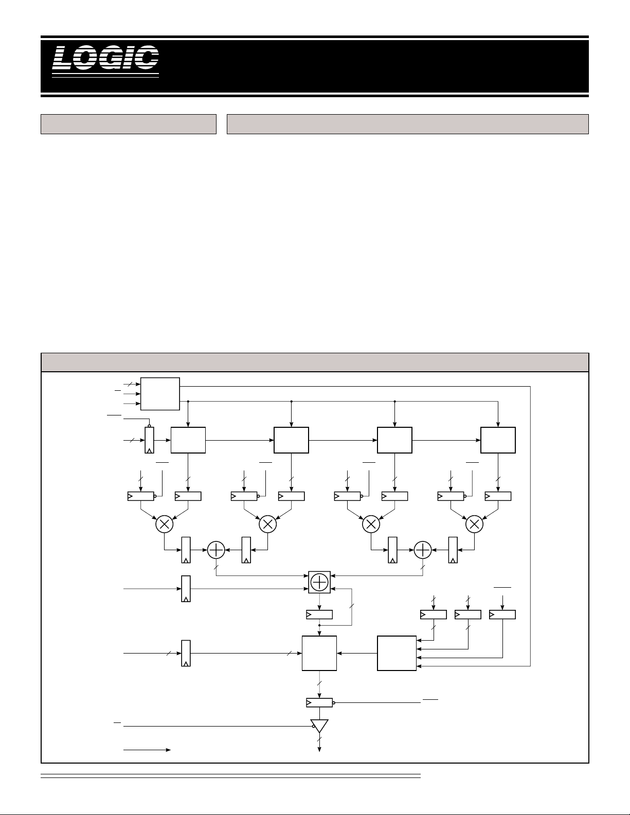
The LF3347 consists of an array of
four 12 x 12-bit registered multipliers
followed by two summers and a
32-bit accumulator. The LF3347
provides four 256 x 12-bit coefficient
banks which are capable of storing
256 different sets of filter coefficients
for the multiplier array. All multiplier data inputs are user accessible
and can be updated every clock cycle
with two’s complement data. The
pipelined architecture has fully
registered input and output ports and
an asynchronous three-state output
enable control to simplify the design
of complex systems.
LF3347 BLOCK DIAGRAM
12
CC
11-0
LD
CCCLK
ENBA
A
7-0
INTERFACE
8
LF
Coefficient
Bank 1
(256 x 12-bit)
Coefficient
Bank 2
(256 x 12-bit)
Coefficient
Bank 3
(256 x 12-bit)
A 32-bit accumulator allows cumulative word growth which may be
internally rounded to 16-bits. Output
data is updated every clock cycle and
may be held under user control. The
data inputs/outputs and control
inputs are registered on the rising
edge of CLK. The Control/Coefficient Data Input, CC11-0, is registered
on the rising edge of CCCLK.
The LF3347 is ideal for performing
pixel interpolation in image manipulation and filtering applications. The
LF3347 can perform a bilinear interpolation of an image (4-pixel kernels)
at real-time video rates when used
Coefficient
Bank 4
(256 x 12-bit)
D1
11-0
ENB
1
12 12
2222
ACC
SHIFT
4-0
OE
CLK TO ALL REGISTERS
3
5
5
25
D2
11-0
ENB
2
12 12
D3
11-0
ENB
3
12 12
32
Rounding
5
Selecting
Limiting
Circuit
16
16
S
15-0
Rounding/
Limiting
Registers
NOTE: NUMBERS IN REGISTERS INDICATE
D4
11-0
ENB
4
12 12
25
LMTENSELLMT
SELRND
3-0
4 4
466
4 4
OCEN
NUMBER OF PIPELINE DELAYS
3-0
Video Imaging Products
1
08/16/2000–LDS.3347-G
Page 2
DEVICES INCORPORATED
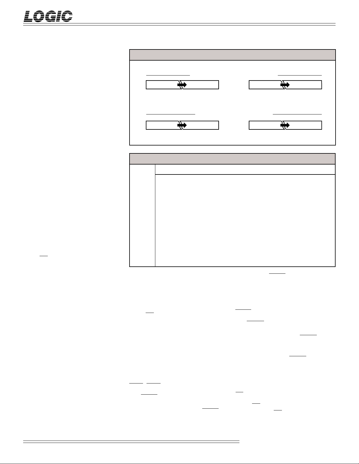
11 10 9 2 1 0
–2
0
(Sign)
2–12
–2
2–92
–102–11
11 10 9 2 1 0
–2
0
(Sign)
2–12
–2
2–92
–102–11
11 10 9 2 1 0
–2
11
(Sign)
2102
9
22212
0
11 10 9 2 1 0
–2
11
(Sign)
2102
9
22212
0
Fractional Two's Complement
Integer Two's Complement
Data Coefficient
LF3347
High-Speed Image Filter with Coefficient RAM
with an image resampling sequencer. Larger kernels or more
complex functions can be realized
by utilizing multiple devices.
Unrestricted access to all data
ports and addressable coefficient
banks provides the LF3347 with
considerable flexibility in applications such as digital filters, adaptive FIR filters, mixers, and other
similar systems requiring highspeed processing.
SIGNAL DEFINITIONS
Power
VCC and GND
+3.3 V power supply. All pins must
be connected.
Clocks
CLK — Master Clock
The rising edge of CLK strobes all
enabled registers.
FIGURE 1. INPUT FORMATS
TABLE 1. OUTPUT FORMATS
SHIFT4-0 S15 S14 S13 · · · S8 S7 · · · S2 S1 S0
00000 F15 F14 F13 · · · F8 F7 · · · F2 F1 F0
00001 F16 F15 F14 · · · F9 F8 · · · F3 F2 F1
00010 F17 F16 F15 · · · F10 F9 · · · F4 F3 F2
· ··· ·· ···
· ··· ·· ···
· ··· ·· ···
01110 F29 F28 F27 · · · F22 F21 · · · F16 F15 F14
CCCLK — Coefficient/Control Clock
When LD is LOW, the rising edge of
CCCLK latches data on CC11-0 into the
device.
Inputs
D111-0 – D411-0 — Data Input
D1–D4 are the 12-bit registered data
input ports. Data is latched on the
rising edge of CLK.
A7-0 — Row Address
A7-0 determines which row in the
coefficient banks feed data to the
multipliers. A7-0 is latched on the
rising edge of CLK. When a new
row address is loaded into the row
address register, data from the
coefficient banks will be latched into
the multiplier input registers on the
next rising edge of CLK.
01111 F30 F29 F28 · · · F23 F22 · · · F17 F16 F15
10000 F31 F30 F29 · · · F24 F23 · · · F18 F17 F16
CC11-0 — Control/Coefficient Data Input
CC11-0 is used to load data into the
coefficient banks and control registers. Data present on CC11-0 is
latched on the rising edge of CCCLK
when LD is LOW.
Outputs
S15-0 — Data Output
S15-0 is the 16-bit registered data
output port.
Controls
ENB1–ENB4 — Data Input Enables
The ENBN (N = 1, 2, 3, or 4) inputs
allow the DN registers to be updated
on each clock cycle. When ENBN is
LOW, data on DN11-0 is latched into
the DN register on the rising edge of
CLK. When ENBN is HIGH, data on
DN11-0 is not latched into the DN
register and the register contents
will not be changed.
ENBA — Row Address Input Enable
The ENBA input allows the row
address register to be updated on
each clock cycle. When ENBA is
LOW, data on A7-0 is latched into
the row address register on the rising
edge of CLK. When ENBA is HIGH,
data on A7-0 is not latched into the
row address register and the register
contents will not be changed.
OE — Output Enable
When OE is LOW, S15-0 is enabled for
output. When OE is HIGH, S15-0 is
placed in a high-impedance state.
Video Imaging Products
2
08/16/2000–LDS.3347-G
Page 3
LF3347
DEVICES INCORPORATED
TABLE 2. REGISTER FORMATS
Register Load Address Bits Register Description A7-0 SELRND3-0 SELLMT3-0
CS0 000H 11-0 Coefficient Set 0 00H
CS1 001H 11-0 Coefficient Set 1 01H
··· · ·
··· · ·
··· · ·
CS255 0FFH 11-0 Coefficient Set 255 FFH
RND0 800H 31-0 Rounding Register 0 0 0 0 0
RND1 801H 31-0 Rounding Register 1 0 0 0 1
··· · ·
··· · ·
··· · ·
RND15 80FH 31-0 Rounding Register 15 1 1 1 1
LMT0 C00H 31-16/15-0 Upper / Lower Limit Register 0 0 0 0 0
LMT1 C01H 31-16/15-0 Upper / Lower Limit Register 0 0 0 0 1
··· · ·
··· · ·
··· · ·
LMT15 C0FH 31-16/15-0 Upper / Lower Limit Register 15 1 1 1 1
High-Speed Image Filter with Coefficient RAM
OCEN — Output Clock Enable
When OCEN is LOW, the output
register is enabled for data loading.
When OCEN is HIGH, output register
loading is disabled and the register’s
contents will not change.
ACC — Accumulator Control
The ACC input determines whether
internal accumulation is performed. If
ACC is LOW, no accumulation is
performed, the prior accumulated sum
is cleared, and the current sum of
products is output. When ACC is
HIGH, the emerging product is added
to the sum of the previous products.
LD — Load Control
LD enables the loading of data into the
coefficient banks and control registers
(control registers are the round and limit
registers). When LD is LOW, data on
CC11-0 is latched into the device on the
rising edge of CCCLK. When LD is
HIGH, data cannot be loaded into the
coefficient banks and control registers.
When enabling the input circuitry for
data loading, the LF3347 requires a
HIGH to LOW transition of LD in order
to function properly. Therefore, LD
needs to be set HIGH immediately after
power up to ensure proper operation of
the input circuitry.
It takes five CCCLK clock cycles to load
one coefficient set into the four coefficient
banks or to load one control register.
When the input circuitry is enabled (LD
goes LOW), the first value loaded into the
device on CC11-0 is an address which
determines what will be loaded (see
Table 2). The next four values loaded on
CC11-0 is the data to be loaded into the
coefficient banks or control register (see
Tables 3-5). After the last data value is
loaded, another coefficient bank address
or control register may be loaded by
feeding another address into CC11-0.
When all desired coefficient banks and
control registers are loaded, the input
circuitry must be disabled by setting LD HIGH.
SELRND3-0 — Round Select
SELRND3-0 allows the user to select
which rounding register will be used
in the rounding circuit to round/offset
the data.
SHIFT4-0 — Shift
SHIFT4-0 determines which 16-bits of
the 32-bits from the accumulator are
passed to the output (see Table 1).
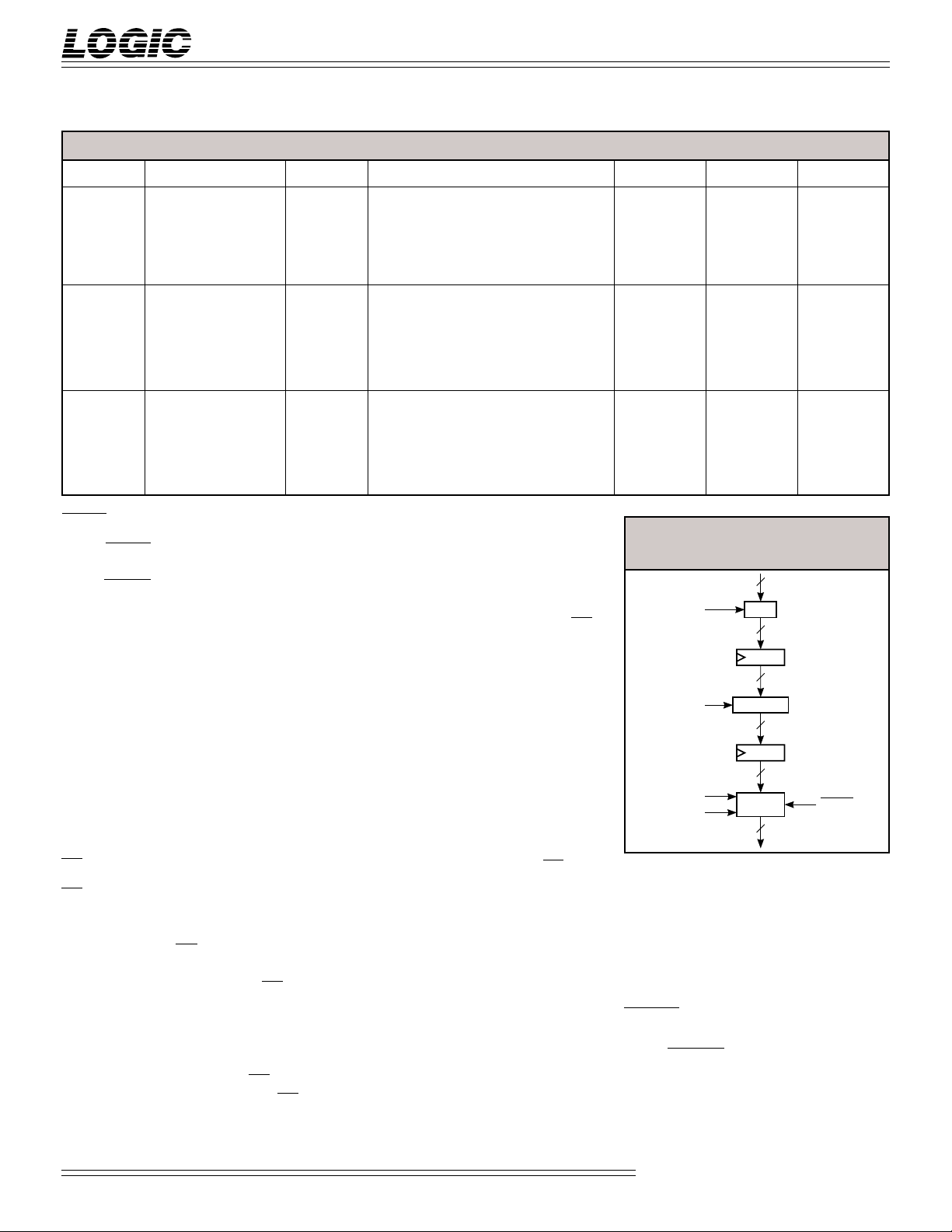
FIGURE 2. ROUNDING, SELECTING,
LIMITING CIRCUITRY
32
RND
31-0
SHIFT
4-0
ULMT
15-0
LLMT
15-0
SELLMT3-0 — Limit Select
SELLMT3-0 allows the user to control
which limiting register will be used in
the limiting circuit to set the upper
and lower limits on the data.
LMTEN — Limit Enable
When LMTEN is LOW, limiting is
enabled and the selected limit register
is used to determine the valid range of
output values for the overall filter.
When HIGH, limiting is disabled.
RND
32
32
SELECT
16
16
LIMIT
16
LMTEN
Video Imaging Products
3
08/16/2000–LDS.3347-G
Page 4

DEVICES INCORPORATED
LF3347
High-Speed Image Filter with Coefficient RAM
FUNCTIONAL DESCRIPTION
Coefficient Banks
The LF3347 has four coefficient banks
which feed coefficient values to the
multipliers. Each bank can store 256
12-bit coefficients. In the example
shown in Table 3, address 10 in coefficient banks 1 through 4 is loaded with
the following values: ABCH, 789H,
456H, 123H. The coefficient banks are
not written to until all four coefficients
have been loaded into the device.
A7-0 determines which coefficient set is
sent to the multipliers. A value of 0 on
A7-0 selects set 0. A value of 1 selects
set 1 and so on.
Rounding/Offset
The accumulator output may be rounded
before being sent to the output select
section. Rounding is user-selectable and
is accomplished by adding the contents of
a round register to the accumulator
output (see Figure 2). There are sixteen
32-bit round registers. In the example in
Table 4, round register 10 is loaded with
76543210H. A round register is not
written to until all four data values have
been loaded into the device.
registers. Each limit register contains both
an upper and lower limit value. The
lower limit is stored in bits 15-0 and the
upper limit is stored in bits 31-16. If the
value fed to the limiting circuitry is less
than the lower limit, the lower limit is
passed to the device output. If the value
fed to the limiting circuitry is greater than
the upper limit, the upper limit is passed
to the device output. When loading limit
values into the device, the upper limit must
be greater than the lower limit. In the
example shown in Table 4, limit register
15 is loaded with a lower limit of 0123H
and an upper limit of 7FEDH. A limit
register is not written to until all four data
values have been loaded into the device.
SELLMT3-0 determines which limit
register is used for limiting. A value of 0
on SELLMT3-0 selects limit register 0. A
value of 1 selects limit register 1 and so on.
TABLE 3. COEFFICIENT BANK LOADING FORMAT
CC11CC10 CC9 CC8 CC7 CC6 CC5 CC4 CC3 CC2 CC1 CC0
1st Word 0000 0000 1010
Address
2nd Word 1010 1011 1100
Bank 1
3rd Word 0111 1000 1001
Bank 2
4th Word 0100 0101 0110
Bank 3
5th Word 0001 0010 0011
Bank 4
TABLE 4. ROUND REGISTER LOADING FORMAT
CC11CC10 CC9 CC8 CC7 CC6 CC5 CC4 CC3 CC2 CC1 CC0
1st Word 1000 0000 1010
Address
2nd Word RRRR 0 0 0 1 0 0 0*0
SELRND3-0 determines which round
register is used for rounding. A value of 0
on SELRND3-0 selects round register 0. A
value of 1 selects round register 1 and so
on. If rounding is not desired, a round
register should be loaded with 0 and
selected as the register for rounding.
Output Select
The filter output word width is 32-bits.
However, only 16-bits may be sent to the
device output. SHIFT4-0 determines
which 16 bits are passed to the device
output (See Table 1).
Output Limiting
An output limiting function is provided
for the output of the filter. When limiting is
enabled (LMTEN LOW), the limit register
selected with SELLMT3-0 determines the
valid range of output values for the overall
filter. There are sixteen 32-bit limit
3rd Word RRRR 0 0 1 1 0 0 1 0
4th Word RRRR 0 1 0 1 0 1 0 0
5th Word RRRR**01 1 1 0 1 1 0
R = Reserved. Must be set to “0”.
* This bit represents the LSB of the Round Register.
** This bit represents the MSB of the Round Register.
TABLE 5. LIMIT REGISTER LOADING FORMAT
CC11CC10 CC9 CC8 CC7 CC6 CC5 CC4 CC3 CC2 CC1 CC0
1st Word 1100 0000 1111
Address
2nd Word RRRR 0 0 1 0 0 0 1 1
3rd Word RRRR *00 0 0 0 0 0 1
4th Word RRRR 1 1 1 0 1 1 0 1
5th Word RRRR**01 1 1 1 1 1 1
R = Reserved. Must be set to “0”.
* This bit represents the MSB of the Lower Limit Register.
** This bit represents the MSB of Upper Limit Register.
Video Imaging Products
4
08/16/2000–LDS.3347-G
Page 5

DEVICES INCORPORATED
LF3347
High-Speed Image Filter with Coefficient RAM
MAXIMUM RATINGS
Storage temperature ........................................................................................................... –65°C to +150°C
Operating ambient temperature........................................................................................... –55°C to +125°C
VCC supply voltage with respect to ground............................................................................ –0.5 V to +4.5V
Input signal with respect to ground .......................................................................................... –0.5 V to 5.5 V
Signal applied to high impedance output ................................................................................. –0.5 V to 5.5 V
Output current into low outputs............................................................................................................. 25 mA
Latchup current ............................................................................................................................... > 400 mA
ESD Classification (MIL-STD-883E METHOD 3015.7) ...................................................................... Class 3
OPERATING CONDITIONS
Active Operation, Commercial 0°C to +70°C 3.00 V ≤ VCC ≤ 3.60 V
Active Operation, Military –55°C to +125°C 3.00 V ≤ VCC ≤ 3.60 V
Above which useful life may be impaired (Notes 1, 2, 3, 8)
To meet specified electrical and switching characteristics
Mode Temperature Range (Ambient) Supply Voltage
ELECTRICAL CHARACTERISTICS
Symbol Parameter Test Condition Min Typ Max Unit
VOH Output High Voltage VCC = Min., IOH = –4 mA 2.4 V
VOL Output Low Voltage VCC = Min., IOL = 8.0 mA 0.4 V
VIH Input High Voltage 2.0 VCC V
VIL Input Low Voltage (Note 3) 0.0 0.8 V
IIX Input Current Ground ≤ VIN ≤ VCC (Note 12) ±10 µA
IOZ Output Leakage Current Ground ≤ VOUT ≤ VCC (Note 12) ±10 µA
ICC1 VCC Current, Dynamic (Notes 5, 6) 150 mA
ICC2 VCC Current, Quiescent (Note 7) 2mA
CIN Input Capacitance TA = 25°C, f = 1 MHz 10 pF
COUT Output Capacitance TA = 25°C, f = 1 MHz 10 pF
Over Operating Conditions (Note 4)
Video Imaging Products
5
08/16/2000–LDS.3347-G
Page 6

DEVICES INCORPORATED
1234567890123456789012345678901212345678901234
1
4
1
4
1
4
1
4
1
4
1
4
1
4
1
4
1
4
1
4
1
4
1
4
1
4
1
4
1
4
1
4
1
4
1
4
1
4
1
4
1
4
1
4
1
4
1
4
1
4
1
4
1
4
1
4
1
4
1
4
1234567890123456789012345678901212345678901234
1234567890123456
1
6
1
6
1
6
1
6
1
6
1
6
1
6
1
6
1
6
1
6
1
6
1
6
1
6
1
6
1
6
1
6
1
6
1
6
1
6
1
6
1
6
1
6
1
6
1
6
1
6
1
6
1
6
1
6
1
6
1
6
1234567890123456
4
SWITCHING CHARACTERISTICS
LF3347
High-Speed Image Filter with Coefficient RAM
COMMERCIAL OPERATING RANGE (0°C to +70°C)
Symbol Parameter Min Max Min Max Min Max
tCYC Cycle Time 25 15 12
tPWL Clock Pulse Width Low 10 7 5
tPWH Clock Pulse Width High 10 7 5
tS Input Setup Time 8 5 3
tH Input Hold Time 0 0 0
tD Output Delay 13 10 8
tDIS Three-State Output Disable Delay (Note 11) 15 12 10
tENA Three-State Output Enable Delay (Note 11) 13 11 8
MILITARY OPERATING RANGE (–55°C to +125°C)
Symbol Parameter Min Max Min Max Min Max
tCYC Cycle Time 25 15 12
tPWL Clock Pulse Width Low 10 7 5
tPWH Clock Pulse Width High 10 7 5
tS Input Setup Time 8 5 3
tH Input Hold Time 0 0 0
tD Output Delay 13 10 8
tDIS Three-State Output Disable Delay (Note 11) 15 12 10
tENA Three-State Output Enable Delay (Note 11) 13 11 8
Notes 9, 10 (ns)
23456789012345
23456789012345
23456789012345
23456789012345
23456789012345
23456789012345
23456789012345
23456789012345
23456789012345
23456789012345
23456789012345
23456789012345
23456789012345
23456789012345
23456789012345
23456789012345
23456789012345
23456789012345
23456789012345
23456789012345
23456789012345
23456789012345
23456789012345
23456789012345
23456789012345
23456789012345
23456789012345
23456789012345
23456789012345
23456789012345
Notes 9, 10 (ns)
23456789012345678901234567890121234567890123
23456789012345678901234567890121234567890123
23456789012345678901234567890121234567890123
23456789012345678901234567890121234567890123
23456789012345678901234567890121234567890123
23456789012345678901234567890121234567890123
23456789012345678901234567890121234567890123
23456789012345678901234567890121234567890123
23456789012345678901234567890121234567890123
23456789012345678901234567890121234567890123
23456789012345678901234567890121234567890123
23456789012345678901234567890121234567890123
23456789012345678901234567890121234567890123
23456789012345678901234567890121234567890123
23456789012345678901234567890121234567890123
23456789012345678901234567890121234567890123
23456789012345678901234567890121234567890123
23456789012345678901234567890121234567890123
23456789012345678901234567890121234567890123
23456789012345678901234567890121234567890123
23456789012345678901234567890121234567890123
23456789012345678901234567890121234567890123
23456789012345678901234567890121234567890123
23456789012345678901234567890121234567890123
23456789012345678901234567890121234567890123
23456789012345678901234567890121234567890123
23456789012345678901234567890121234567890123
23456789012345678901234567890121234567890123
23456789012345678901234567890121234567890123
23456789012345678901234567890121234567890123
25
25
LF3347–
*
15 12
LF3347–
*
15
*
12
*
SWITCHING WAVEFORMS:DATA I/O
CLK
D1
11-0
– D4
11-0
2345678901234567890123
*DISCONTINUED SPEED GRADE
A
CONTROLS
(Except OE)
OE
S
15-0
7-0
123456
t
H
t
S
DN DN+1
AN AN+1
t
DIS
t
PWH
t
CYC
t
ENA
HIGH IMPEDANCE
7
t
PWL
t
D
SN-1
SN
Video Imaging Products
6
08/16/2000–LDS.3347-G
Page 7

DEVICES INCORPORATED
1234567890123456789012345678901212345678901234
1
4
1
4
1
4
1
4
1
4
1
4
1
4
1
4
1
4
1
4
1
4
1
4
1
4
1
4
1
4
1
4
1
4
1
4
1
4
1
4
1
4
1
4
1
4
1
4
1
4
1
4
1234567890123456789012345678901212345678901234
7
7
7
7
7
7
7
7
7
7
7
7
7
7
7
7
7
7
7
7
7
7
7
7
7
7
7
4
LF3347
High-Speed Image Filter with Coefficient RAM
COMMERCIAL OPERATING RANGE (0°C to +70°C)
Symbol Parameter Min Max Min Max Min Max
tCCCYC Control Coefficient Interface Cycle Time 25 15 12
tCCWL Control Coefficient Clock Pulse Width Low 10 7 5
tCCWH Control Coefficient Clock Pulse Width High 10 7 5
tCCENS Control Coefficient Enable Setup Time 8 5 3
tCCENH Control Coefficient Enable Hold Time 0 0 0
tCCS Control Coefficient Data Input Setup Time 8 5 5
tCCH Control Coefficient Data Input Hold Time 0 0 0
MILITARY OPERATING RANGE (–55°C to +125°C)
Symbol Parameter Min Max Min Max Min Max
tCCCYC Control Coefficient Interface Cycle Time 25 15 12
tCCWL Control Coefficient Clock Pulse Width Low 10 7 5
tCCWH Control Coefficient Clock Pulse Width High 10 7 5
tCCENS Control Coefficient Enable Setup Time 8 5 3
tCCENH Control Coefficient Enable Hold Time 0 0 0
tCCS Control Coefficient Data Input Setup Time 8 5 5
tCCH Control Coefficient Data Input Hold Time 0 0 0
Notes 9, 10 (ns)
234567890123456
234567890123456
234567890123456
234567890123456
234567890123456
234567890123456
234567890123456
234567890123456
234567890123456
234567890123456
234567890123456
234567890123456
234567890123456
234567890123456
234567890123456
234567890123456
234567890123456
234567890123456
234567890123456
234567890123456
234567890123456
234567890123456
234567890123456
234567890123456
234567890123456
234567890123456
234567890123456
Notes 9, 10 (ns)
23456789012345678901234567890121234567890123
23456789012345678901234567890121234567890123
23456789012345678901234567890121234567890123
23456789012345678901234567890121234567890123
23456789012345678901234567890121234567890123
23456789012345678901234567890121234567890123
23456789012345678901234567890121234567890123
23456789012345678901234567890121234567890123
23456789012345678901234567890121234567890123
23456789012345678901234567890121234567890123
23456789012345678901234567890121234567890123
23456789012345678901234567890121234567890123
23456789012345678901234567890121234567890123
23456789012345678901234567890121234567890123
23456789012345678901234567890121234567890123
23456789012345678901234567890121234567890123
23456789012345678901234567890121234567890123
23456789012345678901234567890121234567890123
23456789012345678901234567890121234567890123
23456789012345678901234567890121234567890123
23456789012345678901234567890121234567890123
23456789012345678901234567890121234567890123
23456789012345678901234567890121234567890123
23456789012345678901234567890121234567890123
23456789012345678901234567890121234567890123
23456789012345678901234567890121234567890123
25
25
LF3347–
*
15 12
LF3347–
*
15
*
12
*
SWITCHING WAVEFORMS:COEFFICIENT BANK AND CONTROL REGISTER INPUT
CCCLK
t
CCENS
LD
t
CC
11–0
CCS
W: Coefficient Banks/Control Registers written to on this clock cycle.
2345678901234567890123
*DISCONTINUED SPEED GRADE
12 453
t
t
CCWL
t
CCH
ADDRESS C
CCWH
t
SCYC
C
0
6
t
CCENH
1
7
C
2
C
3
Video Imaging Products
W
08/16/2000–LDS.3347-G
Page 8

DEVICES INCORPORATED
OE
0.2 V
t
DIS
t
ENA
0.2 V
1.5 V 1.5 V
3.0V Vth
1
Z
0
Z
Z
1
Z
0
1.5 V
1.5 V
0V Vth
VOL*
V
OH
*
V
OL
*
V
OH
*
Measured V
OL
with IOH = –10mA and IOL = 10mA
Measured V
OH
with IOH = –10mA and IOL = 10mA
NOTES
LF3347
High-Speed Image Filter with Coefficient RAM
1. Maximum Ratings indicate stress
specifications only. Functional operation of these products at values beyond
those indicated in the Operating Conditions table is not implied. Exposure to
maximum rating conditions for extended periods may affect reliability.
2. The products described by this specification include internal circuitry designed to protect the chip from damaging substrate injection currents and accumulations of static charge. Nevertheless, conventional precautions
should be observed during storage,
handling, and use of these circuits in
order to avoid exposure to excessive
electrical stress values.
3. This device provides hard clamping
of transient undershoot. Input levels
below ground will be clamped beginning at –0.6 V. The device can withstand indefinite operation with inputs
or outputs in the range of –0.5 V to
+5.5 V. Device operation will not be
adversely affected, however, input current levels will be well in excess of 100
mA.
9. AC specifications are tested with
input transition times less than 3 ns,
output reference levels of 1.5 V (except
tDIS test), and input levels of nominally
0 to 3.0 V. Output loading may be a
resistive divider which provides for
specified IOH and IOL at an output
voltage of VOH min and VOL max
respectively. Alternatively, a diode
bridge with upper and lower current
sources of IOH and IOL respectively,
and a balancing voltage of 1.5 V may be
used. Parasitic capacitance is 30 pF
minimum, and may be distributed.
This device has high-speed outputs capable of large instantaneous current
pulses and fast turn-on/turn-off times.
As a result, care must be exercised in the
testing of this device. The following
measures are recommended:
a. A 0.1 µF ceramic capacitor should be
installed between VCC and Ground
leads as close to the Device Under Test
(DUT) as possible. Similar capacitors
should be installed between device VCC
and the tester common, and device
ground and tester common.
11. For the tENA test, the transition is
measured to the 1.5 V crossing point
with datasheet loads. For the tDIS test,
the transition is measured to the
±200mV level from the measured
steady-state output voltage with
±10mA loads. The balancing voltage, VTH, is set at 3.0 V for Z-to-0
and 0-to-Z tests, and set at 0 V for Zto-1 and 1-to-Z tests.
12. These parameters are only tested at
the high temperature extreme, which is
the worst case for leakage current.
FIGURE A. OUTPUT LOADING CIRCUIT
DUT
S1
I
OL
V
C
L
I
TH
OH
FIGURE B. THRESHOLD LEVELS
4. Actual test conditions may vary from
those designated but operation is guaranteed as specified.
5. Supply current for a given application can be accurately approximated
by:
2
NCV F
4
where
N = total number of device outputs
C = capacitive load per output
V = supply voltage
F = clock frequency
b. Ground and VCC supply planes
must be brought directly to the DUT
socket or contactor fingers.
c. Input voltages on a test fixture
should be adjusted to compensate for
inductive ground and VCC noise to maintain required DUT input levels relative
to the DUT ground pin.
10. Each parameter is shown as a minimum or maximum value. Input requirements are specified from the point
of view of the external system driving
the chip. Setup time, for example, is
specified as a minimum since the exter-
6. Tested with all outputs changing every cycle and no load, at a 30 MHz clock
rate.
nal system must supply at least that
much time to meet the worst-case requirements of all parts. Responses from
the internal circuitry are specified from
7. Tested with all inputs within 0.1 V of
VCC or Ground, no load.
8. These parameters are guaranteed
but not 100% tested.
the point of view of the device. Output
delay, for example, is specified as a
maximum since worst-case operation of
any device always provides data within
that time.
8
Video Imaging Products
08/16/2000–LDS.3347-G
Page 9

DEVICES INCORPORATED
ORDERING INFORMATION
120-pin
CLK
GND
SELRND3SELRND2
High-Speed Image Filter with Coefficient RAM
SELRND1
SELRND0
ACC
ENB4
D411D410
D49
D48
D47
D46
D45
D44
D43
D42
D41
D40
VCC
GND
ENB3
D311D310
D39
D38
D37
D36
D35
LF3347
SHIFT0
SHIFT1
SHIFT2
SHIFT3
SHIFT4
SELLMT0
SELLMT1
SELLMT2
SELLMT3
LMTEN
OCEN
OE
V
GND
S
S14
S13
S12
S11
S10
120
119
118
117
116
115
114
113
112
111
110
109
108
107
106
105
104
1
2
3
4
5
6
7
8
9
10
11
12
CC
13
14
15
15
16
17
18
19
20
S9
21
S8
22
S7
23
S6
24
S5
25
S4
26
S3
27
S2
28
S1
29
S0
30
3132333435363738394041424344454647484950515253545556575859
11
D19
D18
D17
VCC
GND
ENB1
D110
D1
D16
D15
D14
D13
Top
View
D12
D11
103
D10
VCC
GND
ENB2
999897969594939291
102
101
100
11
D29
D28
D27
D210
D2
90
D34
89
D33
88
D32
D31
87
D30
86
CC11
85
CC10
84
CC9
83
CC8
82
CC7
81
CC6
80
CC5
79
CC4
78
CC3
77
CC2
76
CC1
75
CC0
74
CCCLK
73
LD
72
ENBA
71
GND
70
69
68
67
66
65
64
63
62
61
60
D26
D25
D24
D23
D22
D21
D20
CC
V
A7
A6
A5
A4
A3
A2
A1
A0
Speed
15 ns
12 ns
Plastic Quad Flatpack
(Q1)
0°C to +70°C — COMMERCIAL SCREENING
LF3347QC15
LF3347QC12
Video Imaging Products
9
08/16/2000–LDS.3347-G
Page 10

DEVICES INCORPORATED
1
1
1
1
1
1
1
1
1
1
1
1
1
1
1
1
1
1
1
1
1
1
1
1
1
1
1
1
1
1
1
1
1
1
1
1
1
1
1
1
1
1
1
1
1
1
1
1
1
1
1
1
1
1
1
1
1
1
1
1
1
1
1
1
1
1
1
High-Speed Image Filter with Coefficient RAM
ORDERING INFORMATION
23456789012345678901234567890121234567890123456789012345678901212345678901234567890123456789012
23456789012345678901234567890121234567890123456789012345678901212345678901234567890123456789012
23456789012345678901234567890121234567890123456789012345678901212345678901234567890123456789012
120-pin
23456789012345678901234567890121234567890123456789012345678901212345678901234567890123456789012
23456789012345678901234567890121234567890123456789012345678901212345678901234567890123456789012
23456789012345678901234567890121234567890123456789012345678901212345678901234567890123456789012
23456789012345678901234567890121234567890123456789012345678901212345678901234567890123456789012
23456789012345678901234567890121234567890123456789012345678901212345678901234567890123456789012
23456789012345678901234567890121234567890123456789012345678901212345678901234567890123456789012
23456789012345678901234567890121234567890123456789012345678901212345678901234567890123456789012
23456789012345678901234567890121234567890123456789012345678901212345678901234567890123456789012
23456789012345678901234567890121234567890123456789012345678901212345678901234567890123456789012
23456789012345678901234567890121234567890123456789012345678901212345678901234567890123456789012
23456789012345678901234567890121234567890123456789012345678901212345678901234567890123456789012
23456789012345678901234567890121234567890123456789012345678901212345678901234567890123456789012
23456789012345678901234567890121234567890123456789012345678901212345678901234567890123456789012
23456789012345678901234567890121234567890123456789012345678901212345678901234567890123456789012
23456789012345678901234567890121234567890123456789012345678901212345678901234567890123456789012
23456789012345678901234567890121234567890123456789012345678901212345678901234567890123456789012
23456789012345678901234567890121234567890123456789012345678901212345678901234567890123456789012
23456789012345678901234567890121234567890123456789012345678901212345678901234567890123456789012
23456789012345678901234567890121234567890123456789012345678901212345678901234567890123456789012
23456789012345678901234567890121234567890123456789012345678901212345678901234567890123456789012
23456789012345678901234567890121234567890123456789012345678901212345678901234567890123456789012
23456789012345678901234567890121234567890123456789012345678901212345678901234567890123456789012
23456789012345678901234567890121234567890123456789012345678901212345678901234567890123456789012
23456789012345678901234567890121234567890123456789012345678901212345678901234567890123456789012
23456789012345678901234567890121234567890123456789012345678901212345678901234567890123456789012
23456789012345678901234567890121234567890123456789012345678901212345678901234567890123456789012
23456789012345678901234567890121234567890123456789012345678901212345678901234567890123456789012
23456789012345678901234567890121234567890123456789012345678901212345678901234567890123456789012
23456789012345678901234567890121234567890123456789012345678901212345678901234567890123456789012
23456789012345678901234567890121234567890123456789012345678901212345678901234567890123456789012
23456789012345678901234567890121234567890123456789012345678901212345678901234567890123456789012
23456789012345678901234567890121234567890123456789012345678901212345678901234567890123456789012
23456789012345678901234567890121234567890123456789012345678901212345678901234567890123456789012
23456789012345678901234567890121234567890123456789012345678901212345678901234567890123456789012
23456789012345678901234567890121234567890123456789012345678901212345678901234567890123456789012
23456789012345678901234567890121234567890123456789012345678901212345678901234567890123456789012
23456789012345678901234567890121234567890123456789012345678901212345678901234567890123456789012
23456789012345678901234567890121234567890123456789012345678901212345678901234567890123456789012
23456789012345678901234567890121234567890123456789012345678901212345678901234567890123456789012
23456789012345678901234567890121234567890123456789012345678901212345678901234567890123456789012
23456789012345678901234567890121234567890123456789012345678901212345678901234567890123456789012
23456789012345678901234567890121234567890123456789012345678901212345678901234567890123456789012
23456789012345678901234567890121234567890123456789012345678901212345678901234567890123456789012
23456789012345678901234567890121234567890123456789012345678901212345678901234567890123456789012
23456789012345678901234567890121234567890123456789012345678901212345678901234567890123456789012
23456789012345678901234567890121234567890123456789012345678901212345678901234567890123456789012
23456789012345678901234567890121234567890123456789012345678901212345678901234567890123456789012
23456789012345678901234567890121234567890123456789012345678901212345678901234567890123456789012
23456789012345678901234567890121234567890123456789012345678901212345678901234567890123456789012
23456789012345678901234567890121234567890123456789012345678901212345678901234567890123456789012
23456789012345678901234567890121234567890123456789012345678901212345678901234567890123456789012
23456789012345678901234567890121234567890123456789012345678901212345678901234567890123456789012
23456789012345678901234567890121234567890123456789012345678901212345678901234567890123456789012
23456789012345678901234567890121234567890123456789012345678901212345678901234567890123456789012
23456789012345678901234567890121234567890123456789012345678901212345678901234567890123456789012
23456789012345678901234567890121234567890123456789012345678901212345678901234567890123456789012
23456789012345678901234567890121234567890123456789012345678901212345678901234567890123456789012
23456789012345678901234567890121234567890123456789012345678901212345678901234567890123456789012
23456789012345678901234567890121234567890123456789012345678901212345678901234567890123456789012
23456789012345678901234567890121234567890123456789012345678901212345678901234567890123456789012
23456789012345678901234567890121234567890123456789012345678901212345678901234567890123456789012
23456789012345678901234567890121234567890123456789012345678901212345678901234567890123456789012
23456789012345678901234567890121234567890123456789012345678901212345678901234567890123456789012
23456789012345678901234567890121234567890123456789012345678901212345678901234567890123456789012
Speed
0°C to +70°C — COMMERCIAL SCREENING
–55°C to +125°C — COMMERCIAL SCREENING
–55°C to +125°C — MIL-STD-883 COMPLIANT
12345
A
SRND
2
CLK
SRND
B
SHIFT
1
SHIFT
GND
2
C
SHIFT
4
SLMT
SHIFT
0
D
SLMT
1
SLMT
SHIFT
3
E
LMTEN
OCEN
SLMT
F
V
CC
GND
OE
G
S
13
S
S
15
H
S
11
S
12
S
J
S
8
S
9
S
K
S
5
S
7
S
L
S
1
S
4
V
M
GND
S
3
D1
N
ENB
1
S
0
D1
6
ENB
4
D4
10
D4
1
SRND
SRND
0
3
0
3
D4
ACC
7
11
D4
8
D4
9
KEY
2
Top View
Through Package
14
(i.e., Component Side Pinout)
10
6
2
D1
11
7
D1
CC
D1
D1
8
D1
D1
6
D1
10
9
3
5
D1
2
4
D1
1
GND
Discontinued Package
Ceramic Pin Grid Array
10
7 8 9 10 11
D4
D4
6
3
D4
0
GND
D4
4
D4
2
V
CC
D3
11
D4
5
D4
1
ENB
3
D3
8
V
CC
D2
10
D2
6
D2
2
D1
0
D2
11
D2
8
D2
5
ENB
2
D2
9
D2
7
(G4)
12 13
D3
10
D3
7
D3
4
D3
9
D3
6
D3
1
D3
5
D3
3
D3
0
D3
2
CC
11
CC
9
CC
10
CC
8
CC
7
CC
6
CC
5
CC
4
CC
2
CC
1
CC
3
LD
CCCLK
CC
0
D2
D2
7
A
A
3
A
0
1
4
ENBA
GND
V
6
CC
A
A
4
A
5
A
1
A
2
D2
3
D2
0
Video Imaging Products
08/16/2000–LDS.3347-G
LF3347
 Loading...