

Page 1
DEVICES INCORPORATED
LF3320
Horizontal Digital Image Filter
LF3320
DEVICES INCORPORATED
FEATURES DESCRIPTION
❑❑
❑ 83 MHz Data Rate
❑❑
❑❑
❑ 12-bit Data or Coefficients (Expand-
❑❑
able to 24-bit)
❑❑
❑ 32-Tap FIR Filter, Cascadable for
❑❑
More Filter Taps
❑❑
❑ Over 49 K-bits of on-board Memory
❑❑
❑❑
❑ LF InterfaceTM Allows All 256
❑❑
Coefficient Sets to be Updated
Within Vertical Blanking
❑❑
❑ Various Operating Modes: Dual
❑❑
Filter, Single Filter, Double Wide
Data or Coefficient, Matrix Multiplication, and Accumulator Access.
❑❑
❑ Selectable 16-bit Data Output with
❑❑
User-Defined Rounding and Limiting
❑❑
❑ Supports Interleaved Data Streams
❑❑
❑❑
❑ Supports Decimation up to 16:1 for
❑❑
Increasing Number of Filter Taps
❑❑
❑ 3.3 Volt Supply
❑❑
❑❑
❑ 144 Lead PQFP
❑❑
The LF3320 filters digital images in the
horizontal dimension at real-time
video rates. The input and coefficient
data are both 12 bits and in two’s
complement format. The output is also
in two’s complement format and may
be rounded to 16 bits.
The LF3320 is designed to take
advantage of symmetric coefficient
sets. When symmetric coefficient sets
are used, the device can be configured
as a single 32-tap FIR filter or as two
separate 16-tap FIR filters.
When asymmetric coefficient sets are
used, the device can be configured as a
single 16-tap FIR filter or as two
separate 8-tap FIR filters. Multiple
LF3320s can be cascaded to create
larger filters.
Horizontal Digital Image Filter
Interleave/Decimation Registers (I/D
Registers) allow interleaved data to be
fed directly into the device and filtered
without separating the data into
individual data streams.
The LF3320 can handle a maximum of
sixteen data sets interleaved together.
The I/D Registers and on-chip accumulators facilitate using decimation to
increase the number of filter taps.
Decimation of up to 16:1 is supported.
The LF3320 contains enough on-board
memory to store 256 coefficient sets.
Two separate LF InterfacesTM allow all
256 coefficient sets to be updated within
vertical blanking.
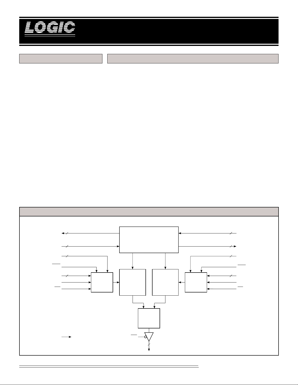
LF3320 BLOCK DIAGRAM
ROUT
CFA
PAUSEA
12 12
11-0
12
11-0
DIN
CENA
11-0
LDA
CLK
8
7-0
12
CAA
256
COEFFICIENT
SET
STORAGE
INTERLEAVE / DECIMATION
REGISTERS
16-TAP
FILTER A
ROUND
SELECT
CIRCUITRY
OED
DOUT
FILTER B
LIMIT
16
15-0
16-TAP
256
COEFFICIENT
SET
STORAGE
RIN
11-0
12
COUT
11-0
8
CAB
7-0
CENB
12
CFB
11-0
PAUSEB
LDB
2-1
Video Imaging Products
08/16/2000–LDS.3320-N
Page 2
DEVICES INCORPORATED
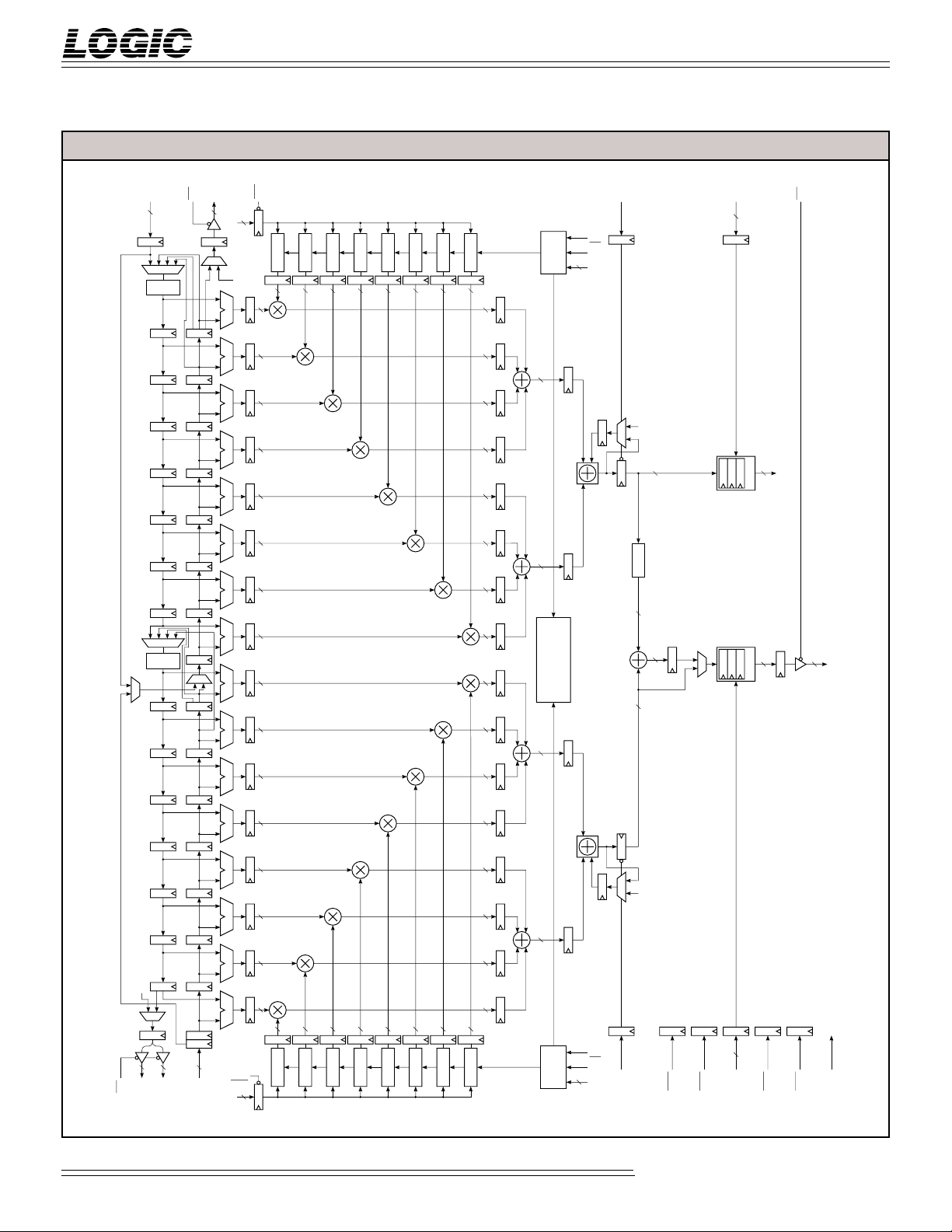
FIGURE 1. LF3320 FUNCTIONAL BLOCK DIAGRAM
LF3320
Horizontal Digital Image Filter
11-0
RIN
12
R
DATA
REVERSAL
1-16
1-16
1-16
1-16
1-16
1-16
1-16
DATA
REVERSAL
1-16
1-16
1-16
11-0
CENB
COUT
OEC
12
7-0
8
CAB
LF
Coef Bank 9
Coef Bank 11
Coef Bank 15
Coef Bank 14
Coef Bank 13
IEO
1-16
1-16
1-16
1-16
1-16
1-16
1-16
IEOS
1-16
1-16
1-16
1-16
11-0
RSLB
ALU
AB
ALU
AB
ALU
AB
ALU
AB
ALU
AB
ALU
AB
ALU
AB
ALU
AB
ALU
AB
ALU
AB
ALU
AB
OUT
12
12
13
13
13
13
13
13 13
13
13
13
13
Coef Bank 12
12
12
Coef Bank 10
12
12
Coef Bank 8
12
12
25
25
25
25
25
25
25
25
25
25
25
FILTER B
INTERFACE
27
27
CONFIGURATION AND
CONTROL REGISTERS
27
ACCB
LDB
PAUSEB
CFB
11-0
12
"0"
32
ACCM B
SCALE
32
32
32
4
ROUND
ROUND
3-0
RSLB
SELECT
SELECT
LIMIT
LIMIT
FILTER B
FILTER A
16
16
15-0
RSLB OUT
OED
15-0
16
DOUT
1-16
FILTER A I/D REGISTERS FILTER B I/D REGISTERS
1-16
1-16
15-12
1-16
RSLB OUT
4
8
3-0
OEC
ROUT
11-4
ROUT
ALU
13
AB
1-16
ALU
13
AB
1-16
ALU
13
AB
1-16
ALU
13
AB
1-16
ALU
13
AB
1-16
12
11-0
DIN
12
CENA
Coef Bank 0
7-0
8
CAA
12
Coef Bank 1
12
Coef Bank 2
12
Coef Bank 3
12
Coef Bank 4
12
Coef Bank 5
12
Coef Bank 6
12
Coef Bank 7
25
25
25
27
25
25
FILTER A
LF
INTERFACE
ACCM A
"0"
LDA
PAUSEA
CFA
11-0
ACCA
12
TXFRA
TXFRB
4
3-0
RSLA
SHENA
SHENB
CLK
Video Imaging Products
2-2
08/16/2000–LDS.3320-N
Page 3
DEVICES INCORPORATED
LF3320
Horizontal Digital Image Filter
SIGNAL DEFINITIONS
Power
VCC and GND
+3.3 V power supply. All pins must be
connected.
Clock
CLK — Master Clock
The rising edge of CLK strobes all
enabled registers.
Inputs
DIN
11-0 — Data Input
11-0 is the 12-bit data input port to
DIN
Filter A. In Dual Filter Mode, DIN11-0
can also be the 12-bit input port to
Filter B. Data is latched on the rising
edge of CLK.
RIN11-0 — Reverse Cascade Input
In Single Filter Mode, RIN11-0 is the 12bit reverse cascade input port. This
port is connected to ROUT11-0 of
another LF3320. In Dual Filter Mode,
RIN11-0 can be the 12-bit input port to
Filter B. Data is latched on the rising
edge of CLK.
CFA11-0 — Coefficient A Input
CFA11-0 is used to load data into the
Filter A coefficient banks (banks 0
through 7) and the configuration/
control registers. Data present on
CFA11-0 is latched into the Filter A LF
InterfaceTM on the rising edge of CLK
when LDA is LOW (see the LF
InterfaceTM section for a full discussion).
CAA7-0 — Coefficient Address A
CAA7-0 determines which row of data
in coefficient banks 0 through 7 is fed
to the multipliers. CAA7-0 is latched
into Coefficient Address Register A on
the rising edge of CLK when CENA is
LOW.
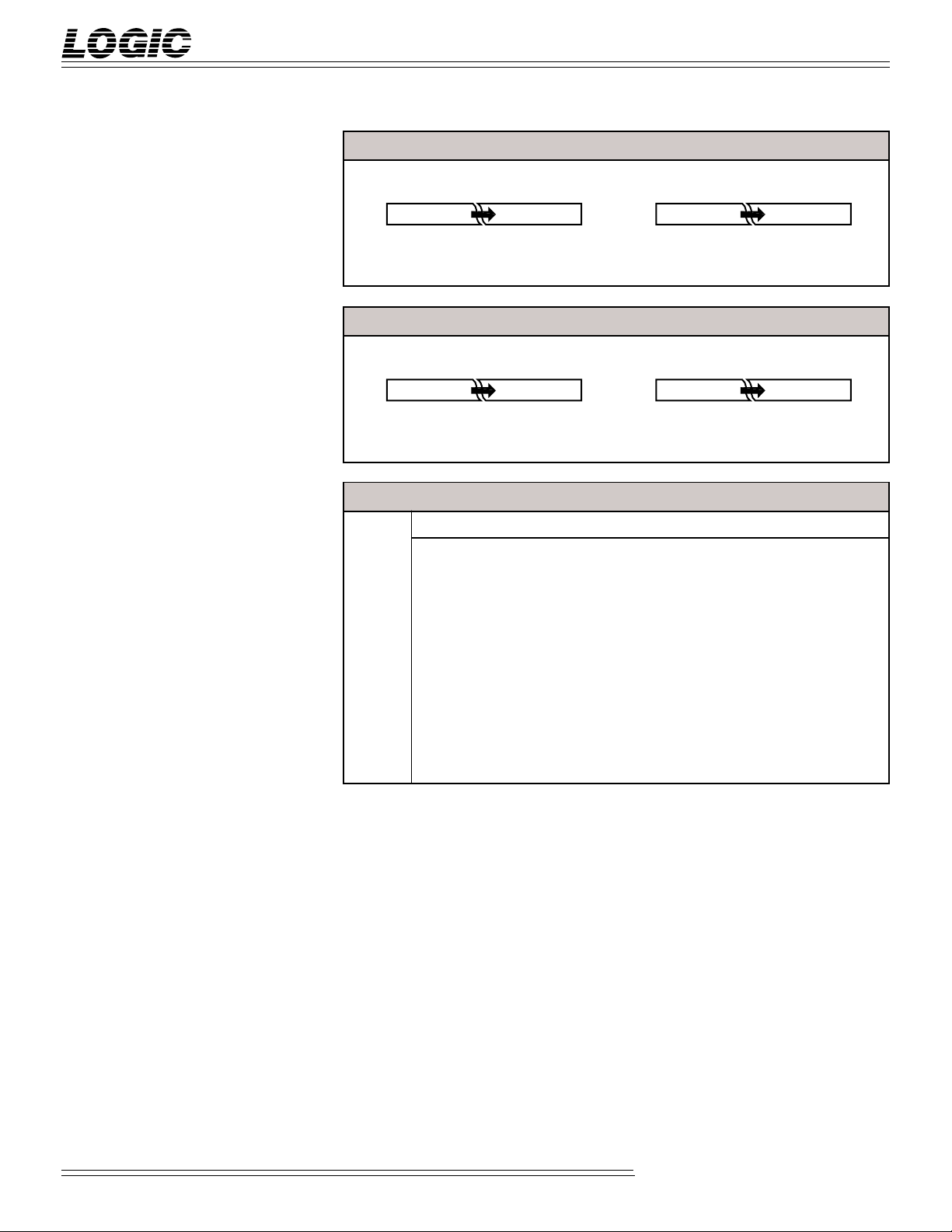
FIGURE 2. INPUT FORMATS
Input Data Coefficient Data
11 10 9 2 1 0
11
–2
(Sign)
2102
9
22212
0
11 10 9 2 1 0
–2
(Sign)
0
2–12
–2
2–92
–102–11
FIGURE 3. ACCUMULATOR OUTPUT FORMATS
Accumulator A Output Accumulator B Output
31 30 29 2 1 0
20
–2
(Sign)
2192
18
2–92
–102–11
31 30 29 2 1 0
–2
(Sign)
20
2192
18
2–92
–102–11
TABLE 1. OUTPUT FORMATS
SLCT4-0 S15 S14 S13 · · · S8 S7 · · · S2 S1 S0
00000 F15 F14 F13 · · · F8 F7 · · · F2 F1 F0
00001 F16 F15 F14 · · · F9 F8 · · · F3 F2 F1
00010 F17 F16 F15 · · · F10 F9 · · · F4 F3 F2
· ··· ·· ···
· ··· ·· ···
· ··· ·· ···
01110 F29 F28 F27 · · · F22 F21 · · · F16 F15 F14
01111 F30 F29 F28 · · · F23 F22 · · · F17 F16 F15
10000 F31 F30 F29 · · · F24 F23 · · · F18 F17 F16
CFB11-0 — Coefficient B Input
CFB11-0 is used to load data into the
Filter B coefficient banks (banks 8
through 15) and the configuration/
control registers. Data present on
CFB11-0 is latched into the Filter B LF
InterfaceTM on the rising edge of CLK
when LDB is LOW (see the LF
InterfaceTM section for a full discussion).
CAB7-0 — Coefficient Address B
CAB7-0 determines which row of data in
coefficient banks 8 through 15 is fed to the
multipliers. CAB7-0 is latched into
Coefficient Address Register B on the
rising edge of CLK when CENB is LOW.
Outputs
DOUT15-0 — Data Output
DOUT15-0 is the 16-bit registered data
output port for the overall filter (Single
Filter Mode) or Filter A (Dual Filter
Mode).
COUT11-0 — Cascade Output
In Single Filter Mode, COUT11-0 is a
12-bit registered cascade output port.
COUT11-0 should be connected to
DIN11-0 of another LF3320. In Dual
Filter Mode, COUT11-0 is a 12-bit
registered output port for the lower
twelve bits of the 16-bit Filter B output.
2-3
Video Imaging Products
08/16/2000–LDS.3320-N
Page 4

DEVICES INCORPORATED
LF3320
Horizontal Digital Image Filter
ROUT11-0 — Reverse Cascade Output
In Single Filter Mode, ROUT
11-0 is a
12-bit registered cascade output port.
ROUT11-0 on one device should be
connected to RIN11-0 of another LF3320.
In Dual Filter Mode, ROUT3-0 is a 4-bit
registered output port for the upper four
bits of the 16-bit Filter B output. In this
mode, ROUT11-4 is disabled.
Controls
LDA — Coefficient A Load
When LDA is LOW, data on CFA11-0 is
latched into the Filter A LF Interface
TM
on the rising edge of CLK. When LDA is
HIGH, data is not loaded into the Filter
A LF InterfaceTM. When enabling the LF
InterfaceTM for data input, a HIGH to
LOW transition of LDA is required in
order for the input circuitry to function
properly. Therefore, LDA must be set
HIGH immediately after power up to
ensure proper operation of the input
circuitry (see the LF Interface
TM
section
for a full discussion).
CENA — Coefficient Address Enable A
When CENA is LOW, data on CAA7-0
is latched into Coefficient Address
Register A on the rising edge of CLK.
When CENA is HIGH, data on CAA 7-0
is not latched and the register’s
contents will not be changed.
LDB — Coefficient B Load
When LDB is LOW, data on CFB11-0 is
latched into the Filter B LF Interface
TM
on the rising edge of CLK. When LDB is
HIGH, data is not loaded into the Filter
B LF InterfaceTM. When enabling the LF
InterfaceTM for data input, a HIGH to
LOW transition of LDB is required in
order for the input circuitry to function
properly. Therefore, LDB must be set
HIGH immediately after power up to
ensure proper operation of the input
circuitry (see the LF InterfaceTM section
for a full discussion).
CENB — Coefficient Address Enable B
When CENB is LOW, data on CAB7-0
is latched into Coefficient Address
Register B on the rising edge of CLK.
When CENB is HIGH, data on CAB7-0
is not latched and the register’s
contents will not be changed.
TXFRA — Filter A LIFO Transfer
Control
TXFRA is used to change which LIFO
in the data reversal circuitry sends
data to the reverse data path and
which LIFO receives data from the
forward data path in Filter A. When
TXFRA goes LOW, the LIFO sending
data to the reverse data path becomes
the LIFO receiving data from the
forward data path, and the LIFO
receiving data from the forward data
path becomes the LIFO sending data to
the reverse data path. The device must
see a HIGH to LOW transition of
TXFRA in order to switch LIFOs.
TXFRA is latched on the rising edge of
CLK.
TXFRB — Filter B LIFO Transfer
Control
TXFRB is used to change which LIFO
in the data reversal circuitry sends
data to the reverse data path and
which LIFO receives data from the
forward data path in Filter B. When
TXFRB goes LOW, the LIFO sending
data to the reverse data path becomes
the LIFO receiving data from the
forward data path, and the LIFO
receiving data from the forward data
path becomes the LIFO sending data to
the reverse data path. The device must
see a HIGH to LOW transition of
TXFRB in order to switch LIFOs.
TXFRB is latched on the rising edge of
CLK.
ACCA — Accumulator A Control
When ACCA is HIGH, Accumulator A
is enabled for accumulation and the
Accumulator A Output Register is
disabled for loading. When ACCA is
LOW, no accumulation is performed
and the Accumulator A Output Register
is enabled for loading. ACCA is latched
on the rising edge of CLK.
ACCB — Accumulator B Control
When ACCB is HIGH, Accumulator B
is enabled for accumulation and the
Accumulator B Output Register is
disabled for loading. When ACCB is
LOW, no accumulation is performed
and the Accumulator B Output Register is enabled for loading. ACCB is
latched on the rising edge of CLK.
SHENA — Filter A Shift Enable
In Dual Filter Mode, SHENA enables
or disables the loading of data into the
Input (DIN11-0) and Filter A I/D
Registers. When SHENA is LOW, data
is latched into the Input/Cascade
Registers and shifted through the I/D
Registers on the rising edge of CLK.
When SHENA is HIGH, data can not
be loaded into the Input/Cascade
Registers or shifted through the I/D
Registers and their contents will not be
changed.
In Single Filter Mode, SHENA also
enables or disables the loading of data
into the Reverse Cascade Input (RIN11-
0), Cascade Output (COUT11-0), Reverse
Cascade Output (ROUT11-0) and Filter B
I/D Registers. It is important to note
that in Single Filter Mode, both SHENA
and SHENB should be connected
together. Both must be active to enable
data loading in Single Filter Mode.
SHENA is latched on the rising edge of
CLK.
SHENB — Filter B Shift Enable
In Dual Filter Mode, SHENB enables or
disables the loading of data into the
Reverse Cascade Input (RIN11-0),
Cascade Output (COUT11-0), Reverse
Cascade Output (ROUT3-0) and Filter B
I/D Registers. When SHENB is LOW,
data is latched into the Cascade Registers and shifted through the I/D
2-4
Video Imaging Products
08/16/2000–LDS.3320-N
Page 5
DEVICES INCORPORATED
LF3320
Horizontal Digital Image Filter
Registers on the rising edge of CLK.
When SHENB is HIGH, data can not be
loaded into the Cascade Registers or
shifted through the I/D Registers and
their contents will not be changed.
In Single Filter Mode, SHENB also
enables or disables the loading of data
into the Input (DIN
11-0), Reverse
Cascade Output (ROUT11-0) and Filter
A I/D Registers. It is important to note
that in Single Filter Mode, both
SHENA and SHENB should be
connected together. Both must be
active to enable data loading in Single
Filter Mode. SHENB is latched on the
rising edge of CLK.
RSLA
3-0 — Filter A Round/Select/Limit
Control
RSLA3-0 determines which of the
sixteen user-programmable Round/
Select/Limit registers (RSL registers)
are used in the Filter A RSL circuitry.
A value of 0 on RSLA3-0 selects RSL
register 0. A value of 1 selects RSL
register 1 and so on. RSLA3-0 is
latched on the rising edge of CLK (see
the round, select, and limit sections for
a complete discussion).
RSLB3-0 — Filter B Round/Select/Limit
Control
ROUT3-0 are enabled for output. When
OEC is HIGH, COUT11-0 and ROUT3-0
are placed in a high-impedance state.
TM
PAUSEA — LF Interface
Pause
When PAUSEA is HIGH, the Filter A
LF InterfaceTM loading sequence is
halted until PAUSEA is returned to a
LOW state. This effectively allows the
user to load coefficients and control
registers at a slower rate than the
master clock (see the LF Interface
TM
section for a full discussion).
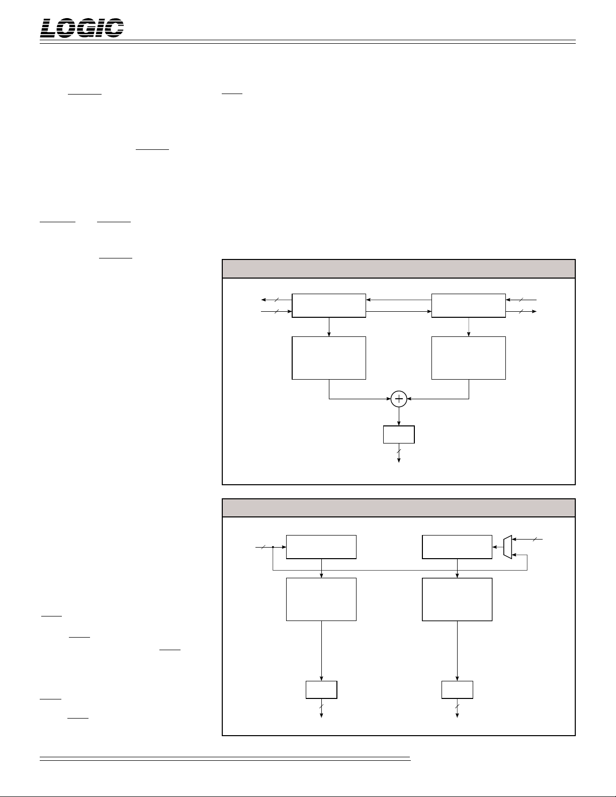
FIGURE 4. SINGLE FILTER MODE
ROUT
DIN
12
11-0
12 12
11-0
I/D
REGISTERS
FILTER
A
PAUSEB — LF Interface
TM
Pause
When PAUSEB is HIGH, the Filter B LF
TM
Interface
loading sequence is halted
until PAUSEB is returned to a LOW
state. This effectively allows the user
to load coefficients and control registers at a slower rate than the master
clock (see the LF InterfaceTM section for
a full discussion).
12
RSL
CIRCUIT
16
DOUT
15-0
I/D
REGISTERS
FILTER
B
RIN
COUT
11-0
11-0
RSLB3-0 determines which of the sixteen
user-programmable RSL registers are
used in the Filter B RSL circuitry. A
value of 0 on RSLB3-0 selects RSL
register 0. A value of 1 selects RSL
register 1 and so on. RSLB3-0 is latched
on the rising edge of CLK (see the round,
select, and limit sections for a complete
discussion).
OED — DOUT Output Enable
When OED is LOW, DOUT15-0 is
enabled for output. When OED is
HIGH, DOUT15-0 is placed in a highimpedance state.
OEC — COUT/ROUT Output Enable
When OEC is LOW, COUT11-0 and
FIGURE 5. DUAL FILTER MODE
DIN
11-0
12
I/D
REGISTERS
FILTER
A
R.S.L.
CIRCUIT
16
DOUT
2-5
15-0
12
RIN
11-0
REGISTERS
ROUT
I/D
FILTER
B
R.S.L.
CIRCUIT
16
3-0
/ COUT
11-0
Video Imaging Products
08/16/2000–LDS.3320-N
Page 6
DEVICES INCORPORATED
LF3320
Horizontal Digital Image Filter
OPERATIONAL MODES
Single Filter Mode
In this mode, the device operates as a
single FIR filter (see Figure 4). It can be
configured to have as many as 32 taps if
symmetric coefficient sets are used. If
asymmetric coefficient sets are used, the
device can be configured to have as
many as 16 taps. Cascade ports are
RIN11-0 or DIN11-0 can be the data
input for Filter B. The Filter B input is
determined by Bit 2 in Configuration
Register 5. DOUT15-0 is the data
output for Filter A. COUT11-0 and
ROUT3-0 together form the data output
for Filter B. COUT11-0 is the twelve
least significant bits and ROUT3-0 is
the four most significant bits of the
16-bit Filter B output.
provided to facilitate cascading multiple
devices to increase the number of filter
taps. Bit 1 in Configuration Register 5
determines the filter mode. In Single
Filter Mode, DIN11-0 is the data input
for the filter and DOUT15-0 is the data
output for the filter.
Dual Filter Mode
In this mode, the device operates as
two separate FIR filters (see Figure 5).
Each filter can be configured to have as
many as 16 taps if symmetric coefficient sets are used. If asymmetric
coefficient sets are used, each filter can
be configured to have as many as 8
taps. In Dual Filter Mode, DIN11-0 is
the data input for Filter A. Either
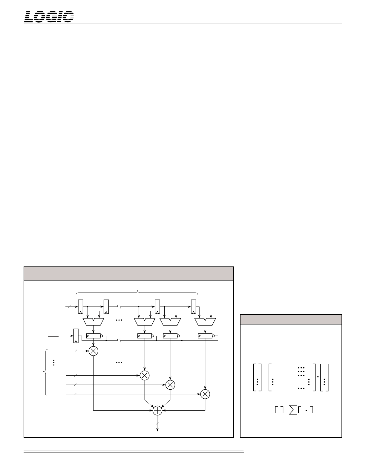
Matrix-vector Multiply Mode
In this mode, the LF3320 can be
configured to multiply a square matrix
of maximum size N (N = 8 or 16),
multiplied by a matrix-vector of
maximum size [8,1] or [16,1]. The
mathematical representation for this
operation is in Figure 7. When configured in the dual filter mode, the LF3320
can process two matrix-vector multipliers simultaneously (i.e. [8x8][8x1]). In
the single filter mode, the LF3320 can
process a single matrix-vector multiply
(i.e. [16x16][16x1]). This mode of
operation allows the user to organize
data values (e.g. pixels) into an array
(e.g. blocks). This function is useful for
any application requiring the opera-
FIGURE 6. MATRIX-VECTOR MULTIPLY MODE
N
12
DIN11-0
RIN11-0
0
tion of matrix multiplication; a function that is used when generating
Discrete Cosine Transform coefficients
(DCT) for the purpose of further
processing.
When configuring the LF3320 for an
[8x8][8x1] matrix-vector operation, the
coefficient banks will require 8 coefficient sets to be loaded into the coefficient
memory banks; each coefficient set will
have 8, 12-bit coefficients. The input
data, [8x1] column-vector, will be loaded
through DIN11-0 for Filter A; either
RIN11-0 or DIN11-0 can be the data
input for Filter B. Conversely, when
configured for a [16x16][16x1]
matrix-vector operation, the coefficient
banks will require 16 coefficient sets to
be loaded into the coefficient memory
banks; each coefficient set will have 16,
12-bit coefficients. The input data,
[16x1] column-vector, will be loaded
through DIN11-0.
To configure the LF3320 for
matrix-vector multiplication, bit 4 of
Configuration Register 5 must be set to
1 (Table 7). The configuration for
single filter mode or dual filter mode
will still apply. Writing 012H or 016H
to Configuration Register 5 will
configure the device for dual filter
mode, [8x8][8x1] matrix-vector multiplication. Subsequently, writing 014H
to Configuration Register 5 will
00
0
configure the device for single filter
N
TXFRA
TXFRB
COEF (N-1)
COEF 2
COEF 1
COEF 0
AB
ALU
12
12
12
12
Dual Filter Mode, N=8
Single FIlter Mode, N=16
AB
ALU
32
AB
ALU
2-6
AB
ALU
FIGURE 7. MATRIX EQUATION
C = COEFFICIENTS
D = DATA INPUT
R = DATA OUTPUT
C
00
0
R
R
1
R
2
R
i
C
01
C
10
C
11
C
20
C
=
21
C
i0
C
i1
R
i
For j=0,1,2,...,(N-1)
=
N=8 or 16
C
C
C
C
(N-1)
i=0
C
0j
02
12
22
i2
C
ij
D
C
C
C
0
1j
D
1
2j
D
2
ij
D
i
D
i
Video Imaging Products
08/16/2000–LDS.3320-N
Page 7
DEVICES INCORPORATED
LF3320
Horizontal Digital Image Filter
mode, [16x16][16x1] matrix-vector
multiplication.
Some functions of the LF3320 must be
disabled when configured for
matrix-vector multiplication. This will
apply to both the single filter mode and
the dual filter mode; these functions
are data reversal and
interleave/decimation. The LF3320
can be cascaded to realize larger
matrices.
Data reversal can be disabled by
setting bit 6, of Configuration Register 1 (Filter A) and Configuration
Register 3 (Filter B), both to 1. The
Odd-Tap, interleave mode will need to
be disabled. Writing a 0 to bit 0 of
Configuration Register 1 and Configuration Register 3 will disable the
odd-tap interleave mode for Filter A
and Filter B. When data is not being
interleaved or decimated, the I/D
Register length should be set to a
length of one (Table 3 and Table 5).
Therefore, writing 040H to Configuration Register 1 and 3 will disable the
data reversal and set the corresponding inherent characteristics for the
desired matrix function.
The Filter A ALU and Filter B ALU are
to be configured for A+B (Table 2 and
Table 4); so that condition A+0 is
satisfied. To accomplish this, bit 0 is to
be reset to 0, bit 1 is to be set to 1, and
bit 2 is to be reset to 0. Writing 002H to
Configuration Register 0 (Filter A) and
Configuration Register 2 (Filter B) will
set the corresponding registers to
satisfy the A+0 condition.
The timing diagrams in Figure 8 and 9
will assume that the Configuration
Registers, the coefficient sets, and the
first set of data values (data set) have
been loaded. Loading input data for an
[8x8][8x1] matrix operation requires 9
clock cycles and loading input data for a
[16x16][16x1] matrix operation requires
17 clock cycles. When configured for an
[8x8][8x1] matrix-vector operation, 8
data values are required for loading.
When configured for a [16x16][16x1]
matrix-vector operation, 16 data values
are required for loading. Each data
value is fed through the I/D Registers,
using the corresponding input.
Once the final data value, of the data
set, has been loaded TXFRA/TXFRB
should be brought LOW for one clock
cycle to complete the loading. Once
this occurs, the data set is then bank
loaded into the respective registers
ready to begin the matrix-vector
multiplication operation. The current
data set will not change until
TXFRA/TXFRB is brought LOW
again. To satisfy the matrix equation (see Figure 7), the current data set
is held for the duration of the required
matrix dimension while cycling
through each coefficient set
(CENA/CENB must be held LOW).
During this time new data values can be
loaded serially, ready for the next
activation of TXFRA/TXFRB. To
insure the correct evaluation of the
matrix-vector multiplication
equation, it is imperative that the
coefficient values are paired with
their corresponding data values.
For the [8x8][8x1] matrix-vector
configuration (dual filter mode), the
first result will appear 19 clock cycles
from the first data input, DIN15-0
(Filter A) and RIN15-0 (Filter B); device
latency for the first result is 10 clock
cycles (10+9 = 19).
The result will appear at the corresponding filter output, DOUT15-0
(Filter A) and ROUT3-0/COUT11-0
(Filter B). For the [16x16][16x1]
matrix-vector configuration (single
filter mode), the first result will appear
FIGURE 8. DUAL FILTER, MATRIX MULTIPLY TIMING SEQUENCE
CLK
DIN
11-0
RIN11-0
CAA7-0
CAB7-0
TXFRA/ TXFRB
ROUT3-0/COUT15-0
DOUT15-0
CENA / CENB
SHENA / SHENB
Data Set 1 with 8 Coefficient Sets
2
1
DATA SET 0
CF00
CF01 CF02
* 8 Clocks - End of First Data/Coefficient Set
** 10 Clocks - First Output of First Data/Coefficient Set
*** 17 Clocks - Final Output of First Data/Coefficient Set
3
CF07
Data Set 2 with 8 Coefficient Sets
9
8*
CF
10 CF11 CF12
2-7
10**
DATA SET 1
OUT
0
11
18
17***
CF20
OUT
CF17
1
OUT
7
OUT
CF21
0
OUT
1
Video Imaging Products
08/16/2000–LDS.3320-N
Page 8
DEVICES INCORPORATED
FIGURE 9. SINGLE FILTER, MATRIX MULTIPLY TIMING SEQUENCE
1 Data Set with 16 Coefficient Sets
LF3320
Horizontal Digital Image Filter
2
1
CLK
DIN
11-0
RIN
11-0
CAA
7-0
CAB
7-0
TXFRA/ TXFRB
DOUT
15-0
CENA / CENB
SHENA / SHENB
* 11 Clocks - First Output of First Data/Coefficient Set
** 16 Clocks - End of First Data/Coefficient Set
*** 26 Clocks - Final Output of First Data/Coefficient Set
CF
DATA SET 0
00
CF01CF
28 clock cycles from the first data
input, DIN15-0; device latency for the
first result is 11 clock cycles
(11+17 = 28). The result will appear at
the corresponding filter output,
DOUT15-0. Subsequently, for both dual
and single filter mode configurations,
the sum of products will continue to
appear every clock cycle thereafter
until the matrix dimension has been
realized. The total pipeline latency for
a complete [8x8][8x1] matrix-vector
operation is 26 clock cycles and the
total pipeline latency for a complete
[16x16][16x1] matrix-vector operation
is 43 clock cycles. Therefore, to process
two square matrices simultaneoulsy, of
size N=8, a total of 73 clock cycles are
all that is required. Similarly, to
process a single square matrix, of size
N=16, a total of 283 clock cycles are
required.
Once again, the timing diagrams (see
Figure 8 and 9) will assume that the
Configuration Registers, the coefficient
sets, and the data values have been
loaded. The corresponding timing
diagram loading sequence for the
coefficient banks and
Configuration/Control registers are
included in the LF3320 data sheets
12
3
02
11*
CF0BCF0CCF
CF
0A
OUT
0
OUT
1
13
DATA SET 0
OUT
2
15 17
14
0D
CF
OUT
3
0E
OUT
16**
CF
0F
OUT
10
5
OUT
6
CF
4
FIGURE 10. DOUBLE WIDE DATA/COEFFICIENT MODE
12
DIN
11-0
12
RIN
11-0
(Figure 11 and Figure 12 respectively).
Further reference to timing diagram
loading sequence for the RSL registers
are also included in the device data
sheet (Figure 15, Figure 14, and Figure
13). The Filter A and Filter B
LF InterfaceTM are used to load data
into the Filter A and Filter B Configuration Registers and coefficient banks.
The Matrix Multiplication Mode is
valid in the Double Wide
I/D
REGISTERS
FILTER
A
R.S.L.
CIRCUIT
16
DOUT
15-0
SCALE
Data/Coefficient Mode. However,
there are some special considerations
when this mode is desired. The
LF3320 must be configured for single
filter mode only, for a maximum (8x8)
matrix. The user must disable the
cascaded filter mode, the accumulator
access mode, and the data reversal
(see Table 7).
Double Wide Data/Coefficient Mode
26***
I/D
REGISTERS
FILTER
B
OUT
15
2-8
Video Imaging Products
08/16/2000–LDS.3320-N
Page 9

DEVICES INCORPORATED
LF3320
Horizontal Digital Image Filter
The LF3320 is capable of supporting
24-bit data and 12-bit coefficients or
12-bit data and 24-bit coefficients.
When configured for this mode of
operation, the Filter B output is scaled
-12
by 2
before adding it to the Filter A
output. This mode of operation is only
valid in single filter mode.
To configure the LF3320 for this mode,
bit 3 of Configuration Register 5 must
be set to 1; this will account for the
scaling function (Table 7). For 24-bit
data, DIN11-0 becomes the MSB
(Filter A) and RIN11-0 becomes the
LSB (Filter B), bit 2 of Configuration
Register 5 must be set to 0. To insure
correct results, the coefficient sets must
be aligned appropriately; that is to say,
the coefficient set used for the MSB
must be the same for the LSB. For
24-bit coefficients, the coefficient banks
for Filter A will correspond to the
coefficient MSB and the coefficient
banks for Filter B will correspond to
the coefficient LSB; therefore, bit 2 must
be set to 1.
Once again, to insure correct results,
the coefficient sets must be aligned
appropriately; that is to say, the MSB
coefficients must correspond to their
LSB coefficients. The output data will
appear at DOUT15-0; output appearing
at ROUT3-0/COUT11-0 will not be of
any value. Bit 1 is set to 0 (for single
filter mode) and bit 0 is set to 0
(cascade mode must be disabled).
Therefore, to realize 24-bit data/12-bit
coefficients the user must write 008H
to Configuration Register 5; conversely,
for 12-bit data/24-bit coefficients the
user must write 00CH to Configuration
Register 5.
The Double Wide Data/Coefficient
Mode is valid in the Matrix Multiplication Mode; however, special considerations must be observed when these
two modes are combined. The LF3320
must be configured for single filter
mode only, for a maximum (8x8)
matrix. In addition, the user must
disable the cascaded filter mode, the
accumulator access mode, and the data
FIGURE 11. ACCUMULATOR ACCESS MODE
12
DIN
11-0
reversal (Table 7). For additional
considerations, refer to the corresponding mode of operation section.
Accumulator Access Mode
Accumulator access allows the user to
accumulate the Filter A output with the
Filter B output. Therefore, this mode is
only valid when the device has been
configured for dual filter operation. To
configure the device for this mode, bit 1
and bit 5 must be set to 1; bit 5 is the
corresponding accumulator access bit
(Table 7). Writing 022H to Configuration Register 5 configures the device to
accumulate the Filter A output with the
Filter B output. All remaining Configuration Registers, 0 through 4 inclusive,
will depend on specific application
requirements (see Tables 2 through 4).
In this mode of operation, the accumulated output is realized at DOUT15-0.
The output data at
ROUT15-0/COUT15-0 is the Filter B
output that is normally expected;
however, the accumulated output data
(DOUT15-0) will be delayed by one
clock cycle, compared to the Filter B
output data.
This type of operation is useful when
two filtered data streams (i.e. I+jQ)
I/D
REGISTERS
FILTER
A
R.S.L.
CIRCUIT
16
DOUT
15-0
need to be accumulated. Such is the
requirement to satisfy the equation,
y(t) = cos(vt)+jsin(vt). The complex
data can be streamed and filtered
using a respective ‘I’ filter and
‘Q’ filter. To convert the complex result
into a real result, as seen at the LF3320
output, two multiplies and one accumulation is required. The cosine and
sine functions are realized through the
coefficient sets; consequently, multiplied by the corresponding ‘I’ and ‘Q’
data streams. To satisfy the remainder
of the equation, Filter A and Filter B
must be accumulated.
As previously stated, this mode of
operation is only valid with the dual
filter mode configuration. All modes of
operation, that are valid in the dual
filter mode, are valid with the accumulator access mode. For additional
considerations, refer to the corresponding mode of operation section.
FUNCTIONAL DESCRIPTION
ALUs
The ALUs double the number of filter
taps available, when symmetric
coefficient sets are used, by pre-adding
data values which are then multiplied
by a common coefficient (see Figure 12).
REGISTERS
CIRCUIT
ROUT
I/D
FILTER
B
R.S.L.
16
3-0
/ COUT
11-0
12
11-0
RIN
2-9
Video Imaging Products
08/16/2000–LDS.3320-N
Page 10

DEVICES INCORPORATED
FIGURE 12. SYMMETRIC COEFFICIENT SET EXAMPLES
12345678
Horizontal Digital Image Filter
5678
1234567
LF3320
1234
Even-Tap, Even-Symmetric
Coefficient Set
FIGURE 13. I/D REGISTER DATA PATHS
REVERSAL
DATA
ALU
COEF 7
COEF 6
AB
ALU
1-16
1-16
AB
1-16
1-16
EVEN-TAP MODE ODD-TAP MODE ODD-TAP INTERLEAVE MODE
Odd-Tap, Even-Symmetric
Coefficient Set
REVERSAL
1-16
1-16
AB
ALU
1-16
1-16
AB
DATA
Delay Stage N–1
Delay Stage N
ALU
COEF 7
COEF 6
Even-Tap, Odd-Symmetric
Coefficient Set
REVERSAL
ALU
DATA
COEF 7
COEF 6
2
1-16
1-16
2
1-16
AB
ALU
1-16
AB
The ALUs can perform two operations:
A+B and B–A. Bit 0 of Configuration
Register 0 determines the operation of
the ALUs in Filter A.
Bit 0 of Configuration Register 2 determines the operation of the ALUs in Filter
B. A+B is used with evensymmetric coefficient sets. B–A is used
with odd-symmetric coefficient sets.
Also, either the A or B operand may be
set to 0. Bits 1 and 2 of Configuration
Register 0 and Configuration Register 2
control the ALU inputs in
Filters A and B respectively. A+0 or B+0
are used with asymmetric coefficient
sets.
Interleave/Decimation Registers
The Interleave/Decimation Registers (I/D
Registers) feed the ALU inputs. They
allow the device to filter up to sixteen data
sets interleaved into the same data stream
without having to separate the data sets.
The I/D Registers should be set to a length
equal to the number of data sets interleaved together.
For example, if two data sets are interleaved together, the I/D Registers should
be set to a length of two. Bits 1 through 4 of
Configuration Register 1 and Configuration Register 3 determine the length of the
I/D Registers in Filters A and B respectively.
The I/D Registers also facilitate using
decimation to increase the number of filter
taps. Decimation by N is accomplished by
reading the filter’s output once every N
2-10
clock cycles. The device supports decimation up to 16:1. With no decimation, the
maximum number of filter taps is sixteen.
When decimating by N, the number of
filter taps becomes 16N because there are
N–1 clock cycles when the filter’s output is
not being read. The extra clock cycles are
used to calculate more filter taps.
When decimating, the I/D Registers
should be set to a length equal to the
decimation factor. For example, when
performing a 4:1 decimation, the I/D
Registers should be set to a length of
four. When decimation is disabled or
when only one data set (non-interleaved
data) is fed into the device, the I/D
Registers should be set to a length of
one.
Video Imaging Products
08/16/2000–LDS.3320-N
Page 11

DEVICES INCORPORATED
LF3320
Horizontal Digital Image Filter
TABLE 2. CONFIGURATION REGISTER 0 – ADDRESS 200H
BITS FUNCTION DESCRIPTION
0 ALU Mode Filter A 0 : A + B
1: B – A
1 Pass A Filter A 0: ALU Input A = 0
1: ALU Input A = Forward Register Path
2 Pass B Filter A 0: ALU Input B = 0
1: ALU Input B = Reverse Register Path
11-3 Reserved Should be set to “0”
TABLE 3. CONFIGURATION REGISTER 1 – ADDRESS 201H
BITS FUNCTION DESCRIPTION
0 Filter A Odd-Tap 0 : Odd-Tap Interleave Mode Disabled
Interleave Mode 1 : Odd-Tap Interleave Mode Enabled
4-1 Filter A I/D Register Length 0000 : 1 Register
0001 : 2 Registers
0010 : 3 Registers
0011 : 4 Registers
0100 : 5 Registers
0101 : 6 Registers
0110 : 7 Registers
0111 : 8 Registers
1000 : 9 Registers
1001 : 10 Registers
1010 : 11 Registers
1011 : 12 Registers
1100 : 13 Registers
1101 : 14 Registers
1110 : 15 Registers
1111 : 16 Registers
5 Filter A Tap Number 0: Even Number of Taps
1: Odd Number of Taps
6 Filter A Data Reversal 0: Data Reversal Enabled
1: Data Reversal Disabled
11-7 Reserved Should be set to “0”
I/D Register Data Path Control
The three multiplexers in the I/D
Register data path control how data
is routed through the forward and
reverse data paths.
The forward data path contains the
I/D Registers in which data flows
from left to right in the block diagram
in Figure 1. The reverse data path
contains the I/D Registers in which
data flows from right to left.
In Single or Dual Filter Modes, data
is fed from the forward data path to
the reverse data path as follows.
When the filter is configured for an
even number of taps, data from the
last I/D Register in the forward data
path is fed into the first I/D Register
in the reverse data path (see Figure 13).
When the filter is configured for an
odd number of taps, the data which
will appear at the output of the last
I/D Register in the forward data
path on the next clock cycle is fed
into the first I/D Register in the
reverse data path. Bit 5 in Configuration Register 1 and Configuration
Register 3 configures Filters A and B
respectively for an even or odd
number of taps.
When interleaved data is fed through
the device and an even tap filter is
desired, the filter should be configured
for an even number of taps and the I/D
Register length should match the
number of data sets interleaved together.
When interleaved data is fed through
the device and an odd tap filter is
desired, the filter should be set to
Odd-Tap Interleave Mode. Bit 0 of
Configuration Register 1 and Configuration Register 3 configures Filters A and
B respectively for Odd-Tap Interleave
Mode. When the filter is configured for
Odd-Tap Interleave Mode, data from the
next to last I/D Register in the forward
data path is fed into the first I/D
Register in the reverse data path.
When the filter is configured for an odd
number of taps (interleaved or
non-interleaved modes), the filter is
structured such that the center data
value is aligned simultaneously at the A
and B inputs of the last ALU in the
forward data path. In order to achieve
the correct result, the user must divide
the coefficient by two.
Data Reversal
Data reversal circuitry is placed after the
multiplexers which route data from the
forward data path to the reverse data
path (see Figure 14). When decimating,
the data stream must be reversed in
order for data to be properly aligned at
the inputs of the ALUs.
When data reversal is enabled, the
circuitry uses a pair of LIFOs to reverse
the order of the data sent to the reverse
data path. TXFRA and TXFRB control
the LIFOs in Filters A and B respectively.
When TXFRA/TXFRB goes LOW, the
LIFO sending data to the reverse data
path becomes the LIFO receiving data
from the forward data path, and the LIFO
receiving data from the forward data
path becomes the LIFO sending data to
2-11
Video Imaging Products
08/16/2000–LDS.3320-N
Page 12

DEVICES INCORPORATED
LF3320
Horizontal Digital Image Filter
the reverse data path. The device must
see a HIGH to LOW transition of
TXFRA/TXFR B in order to switch
LIFOs. If decimating by N,
TXFRA/TXFRB should go LOW once
every N clock cycles. When data
reversal is disabled, the circuitry
functions like an I/D Register. When
feeding interleaved data through the
filter, data reversal should be disabled.
Bit 6 of Configuration Register 1 and
FIGURE 14. DATA REVERSAL
TXFRA/TXFRB
LIFO A
LIFO B
1-16
Configuration Register 3 enables or
disables data reversal for Filters A
and B respectively.
Cascading
Three cascade ports are provided to
allow cascading of multiple devices for
more filter taps (see Figure 15).
COUT11-0 of one device should be
connected to DIN11-0 of another device.
ROUT11-0 of one device should be
connected to RIN11-0 of another device.
As many LF3320s as desired may be
cascaded together. However, the
outputs of the LF3320s must be added
together with external adders.
Bit 0 of Configuration Register 5 determines how the device will send data to
the reverse data path when multiple
LF3320s are cascaded together. If a
LF3320 is the last in the cascade chain,
Bit 0 of Configuration Register 5 should
be set to a “0”. This will cause the data
from the end of the forward data path to
be routed to the beginning of the
reverse data path based on how the
filter is configured (even/odd number
of taps or interleave mode). If a LF3320
is not the last in the cascade chain, Bit 0
of Configuration Register 5 should be set
to a “1”. This will cause RIN11-0 to feed
data to the reverse data path. When
not cascading, Bit 0 of Configuration
Register 5 should be set to a “0”.
Special data routing circuitry is used to
feed the COUT and ROUT output
registers. The data routing circuitry is
required to correctly align data in the
forward and reverse data paths as data
passes from one LF3320 to another.
The COUT and ROUT registers are
loaded with data which is two clock
cycles behind the current output of the
I/D Register just before the ROUT or
COUT register. This correctly accounts
for the extra delays added to the forward
and reverse data paths by the
input/output cascade registers.
FIGURE 15. MULTIPLE LF3320S CASCADED TOGETHER
RIN
12
DIN
I/D
REGISTERS
FILTERAFILTER
I/D
REGISTERS
B
RSL
CIRCUIT
16 16 16 16
COUT
ROUT
DIN
I/D
REGISTERS
REGISTERS
FILTERAFILTER
RSL
CIRCUIT
I/D
B
128 TAP RESULT
RIN ROUT
COUT
DIN DIN
I/D
REGISTERS
REGISTERS
FILTERAFILTER
RSL
CIRCUIT
I/D
B
LF3347
2525
RSL
CIRCUIT
16
DATA OUT
LF3320LF3320LF3320
COUT
ROUTRIN
I/D
REGISTERS
REGISTERS
FILTERAFILTER
RSL
CIRCUIT
I/D
B
LF3320
2-12
Video Imaging Products
08/16/2000–LDS.3320-N
Page 13

DEVICES INCORPORATED
LF3320
Horizontal Digital Image Filter
Output Adder
The Output Adder adds the Filter A and
B outputs together when the device is in
Single Filter Mode. If 24-bit data and 12bit coefficients or 12-bit data and 24-bit
coefficients are desired, the LF3320 can
facilitate this by scaling the Filter B
-12
output by 2
before adding it to the
Filter A output. Bit 3 in Configuration
Register 5 determines if the Filter B
output is scaled before being added to
the Filter A output.
the contents of one of the sixteen Filter
A or B round registers to the overall
filter, Filter A, or Filter B outputs (see
Figure 10). The Filter A round registers
are used for the overall filter (Single
Filter Mode) or Filter A (Dual Filter
Mode). The Filter B round registers are
used for Filter B (Dual Filter Mode).
Each round register is 32-bits wide and
user-programmable. This allows the
filter’s output to be rounded to any
precision required. Since any 32-bit
value may be programmed into the
round registers, the device can support
Rounding
The overall filter output (Single Filter
Mode) or Filter A and B outputs (Dual
Filter Mode) may be rounded by adding
complex rounding algorithms as well as
standard Half-LSB rounding. RSLA
determines which of the sixteen
Filter A round registers are used in the
FIGURE 16. FILTER A AND B ROUND/SELECT/LIMIT CIRCUITRY
RSLB
RB0RB15
3-0
4
DATA IN
32
32
RND
DATA IN
32
RND
32
RSLA
4
Filter A rounding circuitry. RSLB3-0
determines which of the sixteen Filter B
round registers are used in the Filter B
rounding circuitry. A value of 0 on
RSLA/RSLB3-0 selects Filter A/B
round register 0. A value of 1 selects
Filter A/B round register 1 and so
on. RSLA/RSLB3-0 may be changed
every clock cycle if desired. This
allows the rounding algorithm to be
changed every clock cycle. This is
useful when filtering interleaved
data. If rounding is not desired, a
round register should be loaded with 0
and selected as the register used for
3-0
rounding. Round register loading is
discussed in the LF InterfaceTM section.
Output Select
The word width of the overall filter,
Filter A, and Filter B outputs is 32-bits.
3-0
However, only 16-bits may be sent to
DOUT15-0 (Single or Dual Filter Modes)
and COUT11-0/ROUT3-0 (Dual Filter
Mode). The Filter A/B select circuitry
determines which 16-bits are passed
(see Table 1). The Filter A/B select
RA0RA15
registers control the Filter A/B select
circuitry. There are sixteen Filter A
and B select registers.
32
SB0SB15
5
SELECT
16 16
LB0LB15
32
LIMIT
FILTER B RSL FILTER A RSL
16
DATA OUT DATA OUT
32
SELECT
LIMIT
16
SA0SA15
5
LA0LA15
32
The Filter A select registers are used for
the overall filter (Single Filter Mode) or
Filter A (Dual Filter Mode). The Filter B
select registers are used for Filter B (Dual
Filter Mode). Each select register is 5 bits
wide and user-programmable. RSLA3-0
determines which of the sixteen Filter A
select registers are used in the Filter A
select circuitry. RSLB3-0 determines
which of the sixteen Filter B select
registers are used in the Filter B select
circuitry. A value of 0 on
RSLA/RSLB3-0 selects Filter A/B select
register 0. A value of 1 selects Filter A/B
select register 1 and so on.
RSLA/RSLB3-0 may be changed every
clock cycle if desired. This allows the
16-bit window to be changed every
clock cycle. This is useful when filtering
interleaved data. Select register loading is discussed in the LF Interface
TM
section.
2-13
Video Imaging Products
08/16/2000–LDS.3320-N
Page 14

DEVICES INCORPORATED
LF3320
Horizontal Digital Image Filter
TABLE 4. CONFIGURATION REGISTER 2 – ADDRESS 202H
BITS FUNCTION DESCRIPTION
0 ALU Mode Filter B 0 : A + B
1: B – A
1 Pass A Filter B 0: ALU Input A = 0
1: ALU Input A = Forward Register Path
2 Pass B Filter B 0: ALU Input B = 0
1: ALU Input B = Reverse Register Path
11-3 Reserved Must be set to “0”
TABLE 5. CONFIGURATION REGISTER 3 – ADDRESS 203H
BITS FUNCTION DESCRIPTION
0 Filter B Odd-Tap 0 : Odd-Tap Interleave Mode Disabled
Interleave Mode 1 : Odd-Tap Interleave Mode Enabled
4-1 Filter B I/D Register Length 0000 : 1 Register
0001 : 2 Registers
0010 : 3 Registers
0011 : 4 Registers
0100 : 5 Registers
0101 : 6 Registers
0110 : 7 Registers
0111 : 8 Registers
1000 : 9 Registers
1001 : 10 Registers
1010 : 11 Registers
1011 : 12 Registers
1100 : 13 Registers
1101 : 14 Registers
1110 : 15 Registers
1111 : 16 Registers
5 Filter B Tap Number 0: Even Number of Taps
1: Odd Number of Taps
6 Filter B Data Reversal 0: Data Reversal Enabled
1: Data Reversal Disabled
11-7 Reserved Must be set to “0”
Output Limiting
An output limiting function is provided for
the overall filter, Filter A, and Filter B
outputs. The Filter A limiting circuitry is
used to limit the overall filter output (Single
Filter Mode) and the Filter A output (Dual
Filter Mode). The Filter B limiting circuitry
is used to limit the Filter B output (Dual
Filter Mode). The Filter A and B limit
registers determine the valid range of
output values for the Filter A and B
limiting circuitry respectively. There are
sixteen 32-bit user-programmable limit
registers for both Filters A and B. The Filter
A limit registers are used for the overall
filter (Single Filter Mode) or Filter A (Dual
Filter Mode). The Filter B limit registers are
used for Filter B (Dual Filter Mode).
RSLA3-0 determines which of the sixteen
Filter A limit registers are used in the Filter
A limit circuitry. RSLB3-0 determines
which of the sixteen Filter B limit
registers are used in the Filter B limit
circuitry. A value of 0 on
RSLA/RSLB3-0 selects Filter A/B limit
register 0. A value of 1 selects Filter A/B
limit register 1 and so on. Each limit
register contains an upper and lower
limit value. If the value fed to the
limiting circuitry is less than the lower
limit, the lower limit value is passed as
the filter output. If the value fed to the
limiting circuitry is greater than the
upper limit, the upper limit value is
passed as the filter output. Bit 1 and 0
in Configuration Register 4 enable and
disable Filter A and B limiting respectively. RSLA/RSLB3-0 may be changed
every clock cycle if desired. This allows
the limit range to be changed every clock
cycle. This is useful when filtering
interleaved data. When loading limit
values into the device, the upper limit
must be greater than the lower limit.
Limit register loading is discussed in the
LF InterfaceTM section.
Coefficient Banks
The coefficient banks store the coefficients which feed into the multipliers
in Filters A and B. There is a separate
bank for each multiplier. Each bank
can hold 256 12-bit coefficients. The
banks are loaded using an LF
InterfaceTM. There is a separate LF
InterfaceTM for the Filter A and B
banks. Coefficient bank loading is
discussed in the LF Interface
TM
section.
Configuration and Control Registers
The configuration registers determine
how the LF3320 operates. Tables 2
through 7 show the formats of the six
configuration registers. There are three
types of control registers: round, select,
and limit. There are sixteen round
registers for Filter A and sixteen for
Filter B. Each register is 32 bits wide.
RSLA3-0 and RSLB3-0 determine which
Filter A and B round registers respectively are used for rounding.
There are sixteen select registers for
Filter A and sixteen for Filter B. Each
register is 5 bits wide. RSLA3-0 and
RSLB3-0 determine which Filter A and B
select registers respectively are used in
the select circuitry.
2-14
Video Imaging Products
08/16/2000–LDS.3320-N
Page 15

DEVICES INCORPORATED
LF3320
Horizontal Digital Image Filter
There are sixteen limit registers for Filter
A and sixteen for Filter B. Each register
is 32-bits wide and stores both an upper
and lower limit value. The lower limit is
stored in bits 15-0 and the upper limit is
stored in bits 31-16. RSLA3-0 and
RSLB3-0 determine which Filter A and B
limit registers respectively are used for
limiting when limiting is enabled.
Configuration and control register
loading is discussed in the LF
InterfaceTM section.
LF Interface
TM
The Filter A and B LF InterfacesTM are
used to load data into the Filter A and B
coefficient banks respectively. They are
also used to load data into the configuration and control registers.
The following section describes how
the Filter A LF InterfaceTM works. The
Filter A and B LF InterfacesTM are
identical in function. If LDA and
CFA11-0 are replaced with LDB and
CFB11-0, the following section will
describe how the Filter B LF Interface
TM
works.
TABLE 6. CONFIGURATION REGISTER 4 – ADDRESS 204H
BITS FUNCTION DESCRIPTION
0 Filter B Limit Enable 0: Limiting Disabled
1: Limiting Enabled
1 Filter A Limit Enable 0: Limiting Disabled
1: Limiting Enabled
11-2 Reserved Must be set to “0”
TABLE 7. CONFIGURATION REGISTER 5 – ADDRESS 205H
BITS FUNCTION DESCRIPTION
0 Cascade Mode 0: Last In Line
1: First or Middle in Line
1 Single/Dual Filter Mode 0 : Single Filter Mode
1: Dual Filter Mode
2 Filter B Input 0: RIN
1: DIN11-0
3 Output Adder Control 0: Filter A + Filter B
1 : Filter A + Filter B (Filter B Scaled by 2
4 Matrix Multiply Mode 0: Disabled
1: Enabled
5 Accumulator Access Mode 0 : Disabled
1: Enabled
11-6 Reserved Must be set to “0”
11-0
-12
)
LDA is used to enable and disable the
Filter A LF InterfaceTM. When LDA goes
LOW, the Filter A LF InterfaceTM is
enabled for data input. The first value
fed into the interface on CFA11-0 is an
address which determines what the
interface is going to load. The three
most significant bits (CFA11-9) determine if the LF InterfaceTM will load
coefficient banks or
Configuration/control registers (see
Table 8). The nine least significant bits
(CFA8-0) are the address for whatever
is to be loaded (see Tables 9 through
14). For example, to load address 15 of
the Filter A coefficient banks, the first
data value into the LF Interface
TM
should be 00FH. To load Filter A limit
register 10, the first data value should
be C0AH. The first address value
should be loaded into the interface on
the same clock cycle that latches the
HIGH to LOW transition of LDA (see
Figures 17 and 18).
The next value(s) loaded into the
interface are the data value(s) which
will be stored in the bank or register
defined by the address value. When
loading coefficient banks, the interface
will expect eight values to be loaded
into the device after the address value.
The eight values are coefficients 0
through 7. When loading configuration or select registers, the interface
will expect one value after the address
value. When loading round or limit
registers, the interface will expect four
values after the address value. Figures
11 and 12 show the data loading
sequences for the coefficient banks and
Configuration/control registers.
Both PAUSEA and PAUSEB allow the
user to effectively slow the rate of data
loading through the LF InterfaceTM.
When PAUSEA is HIGH, the LF
InterfaceTM affecting the data used for
Filter A is held until PAUSEA is
returned to a LOW. When PAUSEB is
HIGH, the LF InterfaceTM affecting the data
used for Filter B is held until PAUSEB is
returned to a LOW. Figures 19 through 22
display the effects of both PAUSEA and
PAUSEB while loading coefficient and
control data.
Table 15 shows an example of loading
data into the coefficient banks. The
following data values are written into
address 10 of coefficient banks 0
through 7: 210H, 543H, C76H, 9E3H,
701H, 832H, F20H, 143H. Table 16
shows an example of loading data into
a Configuration Register. Data value
003H is written into Configuration
Register 4. Table 17 shows an example
of loading data into a round register.
Data value 7683F4A2H is written into
Filter A round register 12.
Table 18 shows an example of loading
data into a select register. Data value
00FH is loaded into Filter A select
register 2. Table 19 shows an example
2-15
Video Imaging Products
08/16/2000–LDS.3320-N
Page 16

DEVICES INCORPORATED
LF3320
Horizontal Digital Image Filter
of loading data into Filter B limit
register 7. Data value 3B60H is loaded
as the lower limit and 72A4H is loaded
as the upper limit.
It takes 9S clock cycles to load S
coefficient sets into the device. Therefore, it takes 2304 clock cycles to load
all 256 coefficient sets. Assuming an
83 MHz clock rate, all 256 coefficient
sets can be updated in less than 27.7 µs,
which is well within vertical blanking
time. It takes 5S clock cycles to load S
round or limit registers. Therefore, it
takes 320 clock cycles to update all
round and limit registers (both Filters A
and B). Assuming an 83 MHz clock
rate, all Filter A and B round/limit
registers can be updated in 3.84 µs.
FIGURE 17. COEFFICIENT BANK LOADING SEQUENCE
COEFFICIENT SET 1 COEFFICIENT SET 2 COEFFICIENT SET 3
CLK
LDA/LDB
CFA/CFB
11-0
W1: Coefficient Set 1 written to coefficient banks during this clock cycle.
W2: Coefficient Set 2 written to coefficient banks during this clock cycle.
W3: Coefficient Set 3 written to coefficient banks during this clock cycle.
ADDR1COEF
0
COEF7ADDR2COEF
W1
The coefficient banks and
Configuration/Control registers are not
loaded with data until all data values
for the specified address are loaded into
the LF InterfaceTM. In other words, the
coefficient banks are not written to until
all eight coefficients have been loaded
into the LF InterfaceTM. A round register is
not written to until all four data values
are loaded.
W2 W3
0
COEF7ADDR3COEF
0
COEF
7
FIGURE 18. CONFIGURATION/CONTROL REGISTER LOADING SEQUENCE
LDA/LDB
CFA/CFB
CONFIG REG ROUND REGISTER LIMIT REGISTER
CLK
11-0
W1: Configuration Register loaded with new data on this rising clock edge.
W2: Select Register loaded with new data on this rising clock edge.
W3: Round Register loaded with new data on this rising clock edge.
W4: Limit Register loaded with new data on this rising clock edge.
ADDR1DATA
SELECT REG
W1
ADDR
1
W2
ADDR
3
2
DATA
1
DATA
1
DATA
2
W3 W4
DATA
DATA
4
3
ADDR
4
DATA
DATA
1
FIGURE 19. COEFFICIENT BANK LOADING SEQUENCE WITH PAUSE IMPLEMENTATION
COEFFICIENT SET 1
CLK
PAUSEA/PAUSEB
LDA/LDB
2
DATA
DATA
4
3
W1
CFA/CFB
ADDR
11-0
W1: Coefficient Set 1 written to coefficient banks during this clock cycle.
1
COEF
0
COEF
2-16
1
COEF
7
Video Imaging Products
08/16/2000–LDS.3320-N
Page 17

DEVICES INCORPORATED
LF3320
Horizontal Digital Image Filter
After the last data value is loaded, the
interface will expect a new address
value on the next clock cycle. After the
next address value is loaded, data
loading will begin again as previously
discussed. As long as data is loaded
into the interface, LDA must remain
LOW. After all desired coefficient banks
and Configuration/Control registers are
loaded with data, the LF Interface
TM
must be disabled. This is done by
setting LDA HIGH on the clock cycle
after the clock cycle which latches the
last data value. It is important that the
LF InterfaceTM remain disabled when
not loading data into it.
The Filter A coefficient banks may only be
loaded with the Filter A LF InterfaceTM and
the Filter B coefficient banks may only be
loaded with the Filter B LF InterfaceTM.
The Configuration and Control
registers may be loaded with either the
Filter A or B LF InterfacesTM.
TM
Since both LF Interfaces
operate
independently of each other, both LF
InterfacesTM can load data into their
respective coefficient banks at the same
time. Or, one LF InterfaceTM can load
the Configuration/Control registers
while the other loads it’s respective
coefficient banks. If both LF
InterfacesTM are used to load a Configuration or Control register at the same
time, the Filter B LF InterfaceTM will be
given priority over the Filter A LF
Interface
TM
. For example, if the Filter A
LF InterfaceTM attempts to load data
into a configuration register at the
same time that the Filter B LF
InterfaceTM attempts to load a Filter A
round register, the Filter B LF
InterfaceTM will be allowed to load the
round register while the Filter A LF
InterfaceTM will not be allowed to load
the configuration register. However,
the Filter A LF InterfaceTM will
continue to function as if the write
occurred.
TABLE 8. CFA/CFB11-9 DECODE
11 10 9 DESCRIPTION
0 0 0 Coefficient Banks
0 0 1 Configuration Registers
0 1 0 Filter A Select Registers
0 1 1 Filter B Select Registers
1 0 0 Filter A Round Registers
1 0 1 Filter B Round Registers
1 1 0 Filter A Limit Registers
1 1 1 Filter B Limit Registers
FIGURE 20. CONFIGURATION AND SELECT REGISTER LOADING SEQUENCE WITH PAUSE IMPLEMENTATION
CONFIGURATION REGISTER
SELECT REGISTER
CLK
W1
PAUSEA/PAUSEB
LDA/LDB
ADDR
CFA/CFB
11-0
W1: Configuration Register loaded with new data on this rising clock edge.
W2: Select Register loaded with new data on this rising clock edge.
1
DATA
1
ADDR
2
FIGURE 21. ROUND REGISTER LOADING SEQUENCE WITH PAUSE IMPLEMENTATION
ROUND REGISTER
CLK
PAUSEA/PAUSEB
LDA/LDB
ADDR
CFA/CFB
11-0
W1: Round Register loaded with new data on this rising clock edge.
1
DATA
1
DATA
2
DATA
3
DATA
1
DATA
W2
W1
4
2-17
Video Imaging Products
08/16/2000–LDS.3320-N
Page 18

DEVICES INCORPORATED
Horizontal Digital Image Filter
FIGURE 22. LIMIT REGISTER LOADING SEQUENCE WITH PAUSE IMPLEMENTATION
LIMIT REGISTER
CLK
PAUSEA/PAUSEB
LDA/LDB
ADDR
CFA/CFB
11-0
W1: Limit Register loaded with new data on this rising clock edge.
1
DATA
1
DATA
2
DATA
LF3320
W1
3
DATA
4
TABLE 9. FLTR. A ROUND REGISTERS
REGISTER ADDRESS (HEX)
0 800
1 801
14 80E
15 80F
TABLE 12. FLTR. B ROUND REGISTERS
REGISTER ADDRESS (HEX)
0 A00
1 A01
14 A0E
15 A0F
TABLE 10. FLTR.A SELECT REGISTERS
REGISTER ADDRESS (HEX)
0 400
1 401
14 40E
15 40F
TABLE 13. FLTR.B SELECT REGISTERS
REGISTER ADDRESS (HEX)
0 600
1 601
14 60E
15 60F
TABLE 11. FLTR. A LIMIT REGISTERS
REGISTER ADDRESS (HEX)
0 C00
1 C01
14 C0E
15 C0F
TABLE 14. FLTR. B LIMIT REGISTERS
REGISTER ADDRESS (HEX)
0 E00
1 E01
14 E0E
15 E0F
2-18
Video Imaging Products
08/16/2000–LDS.3320-N
Page 19

LF3320
DEVICES INCORPORATED
TABLE 15. COEFFICIENT BANK LOADING FORMAT
CFA/B11 CFA/B10 CFA/B9 CFA/B8 CFA/B7 CFA/B6 CFA/B5 CFA/B4 CFA/B3 CFA/B2 CFA/B1 CFA/B0
1st Word - Address 0 0 0000001010
2nd Word - Bank 0 0 0 1000010000
3rd Word - Bank 1 0 1 0101000011
4th Word - Bank 2 1 1 0001110110
5th Word - Bank 3 1 0 0111100011
6th Word - Bank 4 0 1 1100000001
7th Word - Bank 5 1 0 0000110010
8th Word - Bank 6 1 1 1100100000
9th Word - Bank 7 0 0 0101000011
TABLE 16. CONFIGURATION REGISTER LOADING FORMAT
CFA/B11 CFA/B10 CFA/B9 CFA/B8 CFA/B7 CFA/B6 CFA/B5 CFA/B4 CFA/B3 CFA/B2 CFA/B1 CFA/B0
1st Word - Address 0 0 1000000100
Horizontal Digital Image Filter
2nd Word - Data 0 0 0000000011
TABLE 17. ROUND REGISTER LOADING FORMAT
CFA/B11 CFA/B10 CFA/B9 CFA/B8 CFA/B7 CFA/B6 CFA/B5 CFA/B4 CFA/B3 CFA/B2 CFA/B1 CFA/B0
1st Word - Address 1 0 0000001100
2nd Word - Data R RRR10100010*
3rd Word - Data R RRR11110100
4th Word - Data R RRR10000011
5th Word - Data R RRR0**1110110
TABLE 18. SELECT REGISTER LOADING FORMAT
CFA/B11 CFA/B10 CFA/B9 CFA/B8 CFA/B7 CFA/B6 CFA/B5 CFA/B4 CFA/B3 CFA/B2 CFA/B1 CFA/B0
1st Word - Address 0 1 0000000010
2nd Word - Data 0 0 0000001111
TABLE 19. LIMIT REGISTER LOADING FORMAT
CFA/B11 CFA/B10 CFA/B9 CFA/B8 CFA/B7 CFA/B6 CFA/B5 CFA/B4 CFA/B3 CFA/B2 CFA/B1 CFA/B0
1st Word - Address 1 1 1000000111
2nd Word - Data R RRR01100000
3rd Word - Data R RRR0*0111011
4th Word - Data R RRR10100100
5th Word - Data R RRR0**1110010
R = Reserved. Must be set to “0”.
* This bit represents the MSB of the Lower Limit.
** This bit represents the MSB of the Upper Limit.
Video Imaging Products
2-19
08/16/2000–LDS.3320-N
Page 20

DEVICES INCORPORATED
Horizontal Digital Image Filter
MAXIMUM RATINGS Above which useful life may be impaired (Notes 1, 2, 3, 8)
Storage temperature .............................................................................................................. –65°C to +150°C
Operating ambient temperature .............................................................................................. –55°C to +125°C
CC supply voltage with respect to ground.............................................................................. –0.5 V to +4.5 V
V
Input signal with respect to ground ............................................................................................. –0.5 V to 5.5 V
Signal applied to high impedance output .................................................................................... –0.5V to 5.5 V
Output current into low outputs............................................................................................................... 25 mA
Latchup current ................................................................................................................................. > 400 mA
ESD Classification (MIL-STD-883E METHOD 3015.7) ......................................................................... Class 3
OPERATING CONDITIONS To meet specified electrical and switching characteristics
Mode Temperature Range (Ambient) Supply Voltage
Active Operation, Commercial 0°C to +70°C 3.00 V ≤ VCC ≤ 3.60 V
Active Operation, Military –55°C to +125°C 3.00 V ≤ VCC ≤ 3.60 V
LF3320
ELECTRICAL CHARACTERISTICS Over Operating Conditions (Note 4)
Symbol Parameter Test Condition Min Typ Max Unit
VOH Output High Voltage VCC = Min., IOH = –4 mA 2.4 V
VOL Output Low Voltage VCC = Min., IOL = 8.0 mA 0.4 V
VIH Input High Voltage 2. 0 5.5 V
VIL Input Low Voltage (Note 3) 0.0 0.8 V
IIX Input Current Ground ≤ VIN ≤ VCC (Note 12) ±10 µA
IOZ Output Leakage Current Ground ≤ VOUT ≤ VCC (Note 12) ±10 µA
ICC1 VCC Current, Dynamic (Notes 5, 6) 140 mA
ICC2 VCC Current, Quiescent (Note 7) 2mA
CIN Input Capacitance TA = 25°C, f = 1 MHz 1 0 pF
COUT Output Capacitance TA = 25°C, f = 1 MHz 10 pF
2-20
Video Imaging Products
08/16/2000–LDS.3320-N
Page 21

LF3320
7
7
7
7
7
7
7
7
7
7
7
7
7
7
7
7
7
7
7
7
7
7
7
7
7
7
7
7
7
7
7
7
7
7
7
7
7
7
7
7
7
7
7
7
7
7
4
4
DEVICES INCORPORATED
SWITCHING CHARACTERISTICS
COMMERCIAL OPERATING RANGE (0°C to +70°C) Notes 9, 10 (ns)
2345678901234567890123456
2345678901234567890123456
2345678901234567890123456
Symbol Parameter Min Max Min Max Min Max Min Max
tCYC Cycle Time 25 18 15 12
tPWL Clock Pulse Width Low 1 0 8 7 5
tPWH Clock Pulse Width High 10 8 7 5
tS Input Setup Time 8 6 5 4
tH Input Hold Time 0 0 0 0
tSCT Setup Time Control Inputs 8 6 5 4
tHCT Hold Time Control Inputs 0 0 0 0
tSCC Setup Time Coefficient Control Inputs 8 6 5 4
tHCC Hold Time Coefficient Control Inputs 0 0 0 0
tD Output Delay 1 3 11 9 7
tDCC Cascade Output Delay 1 3 11 9 7.5
tDIS Three-State Output Disable Delay (Note 11) 15 13 12 10
tENA Three-State Output Enable Delay (Note 11) 15 13 12 10
2345678901234567890123456
2345678901234567890123456
2345678901234567890123456
2345678901234567890123456
2345678901234567890123456
2345678901234567890123456
2345678901234567890123456
2345678901234567890123456
2345678901234567890123456
2345678901234567890123456
2345678901234567890123456
2345678901234567890123456
2345678901234567890123456
2345678901234567890123456
2345678901234567890123456
2345678901234567890123456
2345678901234567890123456
2345678901234567890123456
2345678901234567890123456
2345678901234567890123456
2345678901234567890123456
2345678901234567890123456
2345678901234567890123456
2345678901234567890123456
2345678901234567890123456
2345678901234567890123456
2345678901234567890123456
2345678901234567890123456
2345678901234567890123456
2345678901234567890123456
2345678901234567890123456
2345678901234567890123456
2345678901234567890123456
2345678901234567890123456
2345678901234567890123456
2345678901234567890123456
2345678901234567890123456
2345678901234567890123456
2345678901234567890123456
2345678901234567890123456
2345678901234567890123456
2345678901234567890123456
2345678901234567890123456
25
*
Horizontal Digital Image Filter
LF3320–
*
18
15 12
SWITCHING WAVEFORMS:DATA I/O
CLK
11-0
DIN
RIN
11-0
CAA
7-0
CAB
7-0
CONTROLS
(Except OED & OEC)
OED
OEC
15-0
DOUT
11-0/
COUT
ROUT
2345678901234567890123
2345678901234567890123
*DISCONTINUED SPEED GRADE
11-0
123456
t
H
t
S
DIN/RIN
N
t
HCC
t
SCC
CAA/CAB
N
t
HCT
t
SCT
DIN/RIN
CAA/CAB
7
t
PWH
t
CYC
t
t
ENA
ENA
PWL
OUTPUTN-
OUTPUTN-
1
1
tD
tDCC
OUTPUT
OUTPUT
N
N
N+1
N+1
t
DIS
t
DIS
t
HIGH IMPEDANCE
HIGH IMPEDANCE
Video Imaging Products
2-21
08/16/2000–LDS.3320-N
Page 22

LF3320
7
7
7
7
7
7
7
7
7
7
7
7
7
7
7
7
7
7
7
7
7
7
7
7
4
4
DEVICES INCORPORATED
COMMERCIAL OPERATING RANGE (0°C to +70°C) Notes 9, 10 (ns)
2345678901234567890123456
2345678901234567890123456
2345678901234567890123456
2345678901234567890123456
Symbol Parameter Min Max Min Max Min Max Min Max
tCFS Coefficient Input Setup Time 8 6 6 5.5
tCFH Coefficient Input Hold Time 0 0 0 0
tLS Load Setup Time 8 7 6 4
tLH Load Hold Time 0 0 0 0
tPS PAUSE Setup Time 8 6 5 4
tPH PAUSE Hold Time 0 0 0 0
2345678901234567890123456
2345678901234567890123456
2345678901234567890123456
2345678901234567890123456
2345678901234567890123456
2345678901234567890123456
2345678901234567890123456
2345678901234567890123456
2345678901234567890123456
2345678901234567890123456
2345678901234567890123456
2345678901234567890123456
2345678901234567890123456
2345678901234567890123456
2345678901234567890123456
2345678901234567890123456
2345678901234567890123456
2345678901234567890123456
2345678901234567890123456
2345678901234567890123456
25
*
Horizontal Digital Image Filter
LF3320–
*
18
15 12
SWITCHING WAVEFORMS: LF INTERFACE
CLK
LDA
LDB
PAUSEA
PAUSEB
CFA
11–0
11–0
CFB
t
LS
t
CFS
12 453
t
t
CYC
CF
PWL
0
ADDRESS
t
PWH
t
CFH
TM
6
t
LH
t
PS
t
PH
CF
1
CF
2
2345678901234567890123
2345678901234567890123
*DISCONTINUED SPEED GRADE
2-22
Video Imaging Products
08/16/2000–LDS.3320-N
Page 23

DEVICES INCORPORATED
OE
0.2 V
t
DIS
t
ENA
0.2 V
1.5 V 1.5 V
3.0V Vth
1
Z
0
Z
Z
1
Z
0
1.5 V
1.5 V
0V Vth
VOL*
V
OH*
V
OL*
V
OH*
Measured V
OL with IOH = –10mA and IOL = 10mA
Measured V
OH with IOH = –10mA and IOL = 10mA
NOTES
LF3320
Horizontal Digital Image Filter
1. Maximum Ratings indicate stress
specifications only. Functional operation of these products at values beyond
those indicated in the Operating Conditions table is not implied. Exposure to
maximum rating conditions for extended periods may affect reliability.
2. The products described by this specification include internal circuitry designed to protect the chip from damaging
substrate injection currents and accumulations of static charge. Nevertheless, conventional precautions should
be observed during storage, handling,
and use of these circuits in order to avoid
exposure to excessive electrical stress
values.
3. This device provides hard clamping
of transient undershoot. Input levels
below ground will be clamped beginning at –0.6 V. The device can withstand
indefinite operation with inputs or outputs in the range of –0.5 V to +5.5 V.
Device operation will not be adversely
affected, however, input current levels
will be well in excess of 100 mA.
input transition times less than 3 ns,
output reference levels of 1.5 V (except
DIS test), and input levels of nominally
t
0 to 3.0 V. Output loading may be a
resistive divider which provides for
specified IOH and IOL at an output
voltage of VOH min and VOL max
respectively. Alternatively, a diode
bridge with upper and lower current
sources of IOH and IOL respectively,
and a balancing voltage of 1.5 V may be
used. Parasitic capacitance is 30 pF
minimum, and may be distributed.
This device has high-speed outputs capable of large instantaneous current
pulses and fast turn-on/turn-off times.
As a result, care must be exercised in the
testing of this device. The following
measures are recom mended:
a. A 0.1 µF ceramic capacitor should be
installed between V
CC and Ground
leads as close to the Device Under Test
(DUT) as possible. Similar capacitors
should be installed between device VCC
and the tester common, and device
ground and tester common.
measured to the 1.5 V crossing point with
datasheet loads. For the t
DIS test, the
transition is measured to the ±200mV
level from the measured steady-state
output voltage with ±10mA loads.
The balancing voltage, V
TH, is set at
3.0 V for Z-to-0 and 0-to-Z tests, and
set at 0 V for Z-to-1 and 1-to-Z tests.
12. These parameters are only tested at
the high temperature extreme, which is
the worst case for leakage current.
FIGURE A. OUTPUT LOADING CIRCUIT
DUT
S1
I
OL
V
C
L
I
TH
OH
FIGURE B. THRESHOLD LEVELS
4. Actual test conditions may vary from
those designated but operation is guaranteed as specified.
5. Supply current for a given application can be accurately approximated
by:
b. Ground and VCC supply planes must
be brought directly to the DUT socket or
contactor fingers.
c. Input voltages on a test fixture should
be adjusted to compensate for inductive
ground and VCC noise to maintain re-
quired DUT input levels relative to the
2
NCV F
where
N = total number of device outputs
C = capacitive load per output
V = supply voltage
F = clock frequency
4
DUT ground pin.
10. Each parameter is shown as a minimum or maximum value. Input requirements are specified from the point of view
of the external system driving the chip.
Setup time, for example, is specified as a
minimum since the external system must
6. Tested with outputs changing every
cycle and no load, at a 40 MHz clock rate.
supply at least that much time to meet the
worst-case requirements of all parts.
Responses from the internal circuitry are
7. Tested with all inputs within 0.1 V of
VCC or Ground, no load.
8. These parameters are guaranteed but
not 100% tested.
9. AC specifications are tested with
specified from the point of view of the
device. Output delay, for example, is
specified as a maximum since worstcase operation of any device always provides data within that time.
11. For the tENA test, the transition is
2-23
Video Imaging Products
08/16/2000–LDS.3320-N
Page 24

DEVICES INCORPORATED
ORDERING INFORMATION
LF3320
Horizontal Digital Image Filter
144-pin
VCC
DIN
DIN
DIN
DIN
DIN
DIN
DIN
DIN
DIN
DIN
DIN
DIN
GND
VCC
CENA
CAA
CAA
CAA
CAA
CAA
CAA
CAA
CAA
CFA
CFA
CFA
CFA
CFA
CFA
CFA
CFA
CFA
CFA
CFA
CFA
GND
ROUT11ROUT10ROUT9ROUT8ROUT7ROUT6ROUT5ROUT4ROUT3ROUT2ROUT1ROUT0GND
144
143
142
141
140
139
138
137
136
1
11
2
10
3
9
4
8
5
7
6
6
7
5
8
4
9
3
10
2
11
1
12
0
13
14
15
16
7
17
6
18
5
19
4
20
3
21
2
22
1
23
0
24
11
25
10
26
9
27
8
28
7
29
6
30
5
31
4
32
3
33
2
34
1
35
0
36
135
3738394041424344454647484950515253545556575859606162636465666768697071
134
133
132
131
VCC
SHENA
TXFRA
GND
130
129
128
127
Top
View
CLK
VCC
TXFRB
SHENB
RIN0RIN1RIN2RIN3RIN4RIN5RIN6RIN7RIN8RIN9RIN10RIN11OEC
126
125
124
123
122
121
120
119
118
117
116
115
114
113
112
111
110
VCC
109
108
107
106
105
104
103
102
101
100
72
GND
11
COUT
COUT
10
COUT
9
COUT
8
COUT
7
COUT
6
COUT
5
COUT
4
COUT
COUT
COUT
COUT
GND
VCC
CENB
CAB
CAB
CAB
CAB
CAB
CAB
CAB
CAB
CFB
CFB
CFB
CFB
CFB
CFB
CFB
CFB
CFB
CFB
CFB
CFB
3
2
1
0
7
6
5
4
3
2
1
0
11
10
9
8
7
6
5
4
3
2
1
0
99
98
97
96
95
94
93
92
91
90
89
88
87
86
85
84
83
82
81
80
79
78
77
76
75
74
73
Speed
15 ns
12 ns
3
LDA
ACCA
RSLA2RSLA1RSLA
RSLA
PAUSEA
0°C to +70°C — COMMERCIAL SCREENING
0
VCC
15
GND
DOUT14DOUT13DOUT12DOUT11DOUT
DOUT
10
DOUT9DOUT
8
GND
Plastic Quad Flatpack
(Q5)
LF3320QC15
LF3320QC12
7
OED
DOUT
DOUT6DOUT5DOUT4DOUT3DOUT2DOUT1DOUT
0
0
3
GND
VCC
RSLB1RSLB2RSLB
RSLB
ACCB
PAUSEB
LDB
2-24
Video Imaging Products
08/16/2000–LDS.3320-N
 Loading...