

Page 1
DEVICES INCORPORATED
LF3310
Horizontal / Vertical Digital Image Filter
LF3310
DEVICES INCORPORATED
Horizontal / Vertical Digital Image Filter
FEATURES DESCRIPTION
❑❑
❑ 83 MHz Data Rate
❑❑
❑❑
❑ 12-bit Data and Coefficients
❑❑
❑❑
❑ On-board Memory for 256 Horizontal
❑❑
and Vertical Coefficient Sets
❑❑
❑ LF InterfaceTM Allows All 512
❑❑
Coefficient Sets to be Updated
Within Vertical Blanking
❑❑
❑ Selectable 12-bit Data Output with
❑❑
User-Defined Rounding and
Limiting
❑❑
❑ Seven 3K x 12-bit, Programmable
❑❑
Two-Mode Line Buffers
❑❑
❑ 16 Horizontal Filter Taps
❑❑
❑❑
❑ 8 Vertical Filter Taps
❑❑
❑❑
❑ Two Operating Modes: Dimension-
❑❑
ally Separate and Orthogonal
❑❑
❑ Supports Interleaved Data Streams
❑❑
❑❑
❑ Horizontal Filter Supports Decima-
❑❑
tion up to 16:1 for Increasing
Number of Filter Taps
❑❑
❑ 3.3 Volt Power Supply
❑❑
❑❑
❑ 5 Volt Tolerant I/O
❑❑
❑❑
❑ 144 Lead PQFP
❑❑
The LF3310 is a two-dimensional digital
image filter capable of filtering data at
real-time video rates. The device
contains both a horizontal and a
vertical filter which may be cascaded or
used concurrently for two-dimensional
filtering. The input, coefficient, and
output data are all 12-bits and in two’s
complement format.
The horizontal filter is designed to take
advantage of symmetric coefficient sets.
When symmetric coefficient sets are
used, the horizontal filter can be
configured as a 16-tap FIR filter. When
asymmetric coefficient sets are used, it
can be configured as an 8-tap FIR filter.
The vertical filter is an 8-tap FIR filter
with all required line buffers contained
on-chip. The line buffers can store
video lines with lengths from 4 to 3076
pixels.
Horizontal filter Interleave/Decimation Registers (I/D Registers) and the
vertical filter line buffers allow
interleaved data to be fed directly into
the device and filtered without
separating the data into individual
data streams. The horizontal filter
can handle a maximum of sixteen
data sets interleaved together. The
vertical filter can handle interleaved
video lines which contain 3076 or less
data values. The I/D Registers and
horizontal accumulator facilitate
using decimation to increase the
number of filter taps in the horizontal
filter. Decimation of up to 16:1 is
supported.
The device has on-chip storage for 256
horizontal coefficient sets and 256
vertical coefficient sets. Each filter’s
coefficients are loaded independently
of each other allowing one filter’s
coefficients to be updated without
affecting the other filter’s coefficients.
In addition, a horizontal or vertical
coefficient set can be updated independently from the other coefficient
sets in the same filter.
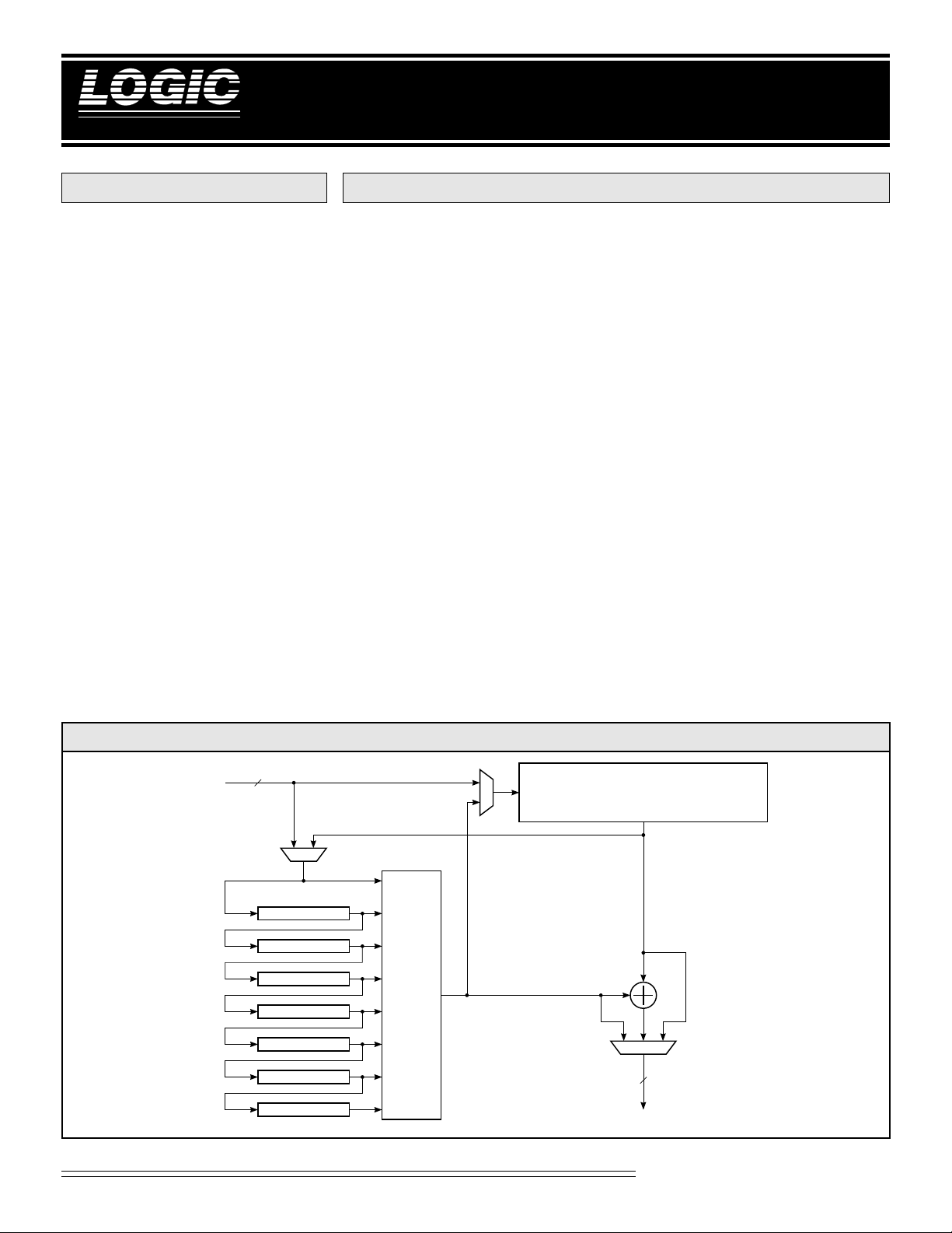
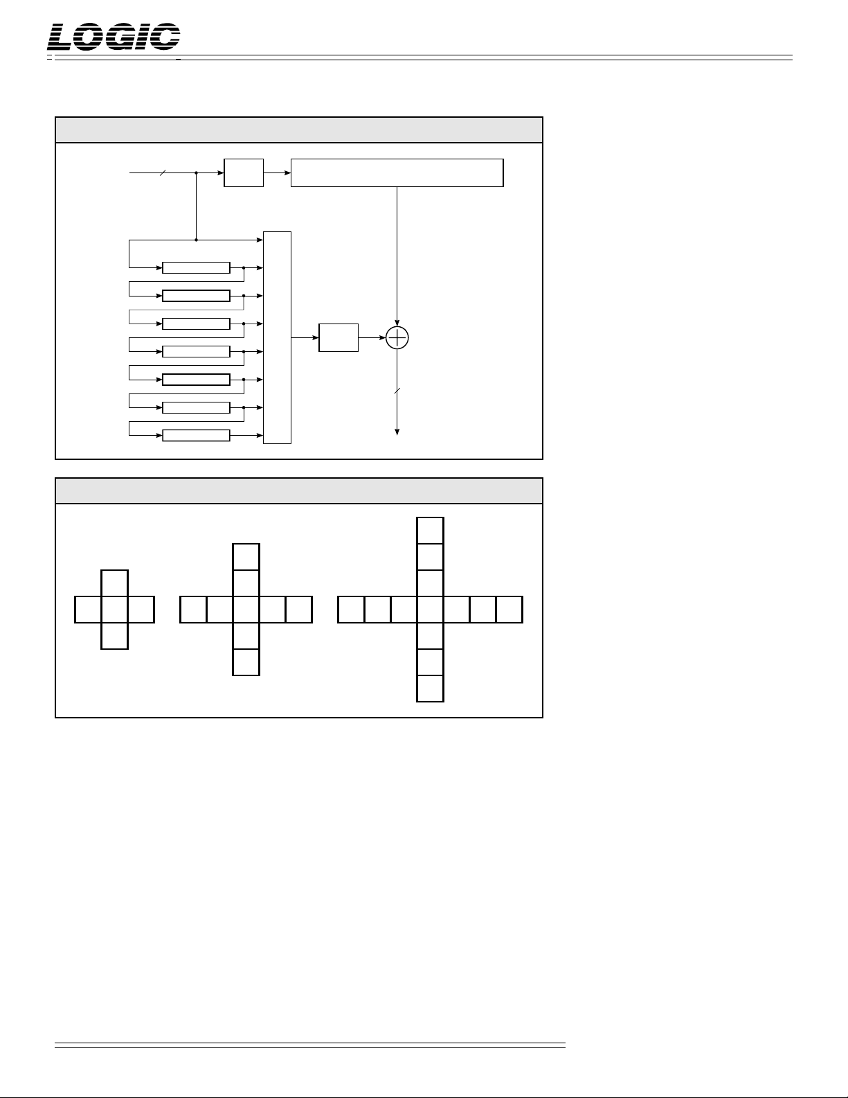
LF3310 BLOCK DIAGRAM
DIN
11-0
12
3K LINE BUFFER
3K LINE BUFFER
3K LINE BUFFER
3K LINE BUFFER
3K LINE BUFFER
3K LINE BUFFER
3K LINE BUFFER
8-TAP VERTICAL FILTER
256 COEFFICIENT SET STORAGE
1
16-TAP HORIZONTAL FILTER
256 COEFFICIENT SET STORAGE
12
DOUT
11-0
Video Imaging Products
11/08/2001-LDS.3310-H
Page 2
DEVICES INCORPORATED
FIGURE 1. LF3310 FUNCTIONAL BLOCK DIAGRAM
LF3310
Horizontal / Vertical Digital Image Filter
IEO
DATA
REVERSAL
1-16
1-16
1-16
1-16
I/D REGISTERS
1-16
1-16
1-16
1-16
1-16
1-16
1-16
1-16
1-16
1-16
1-16
ALU
AB
ALU
AB
ALU
AB
ALU
AB
ALU
AB
ALU
AB
ALU
13 13 13 13 13 13 13
AB
ALU
13
AB
H Coef Bank 7
12
12
H Coef Bank 612H Coef Bank 5
12
12
12
H Coef Bank 4
12
12
3-0
HACC
"0"
32
32
DATA
DELAY
27 27
25 25 25 25 25 25 25 25
26
HRSL
4
LIMIT
3232
ROUND
SELECT
HORIZONTAL
12
LIMIT
ROUND
SELECT
VERTICAL
"0"
26
OE
11-0
12
DOUT
3-0
4
VRSL
VACC
TXFR
DATA
DELAY
H Coef Bank 0
H Coef Bank 1
CONFIGURATION AND
CONTROL REGISTERS
LF
LF
VERTICAL
INTERFACE
HORIZONTAL
12
12
11-0
11-0
DIN
HCF
HPAUSE
INTERFACE
12
11-0
VLD
HLD
VCF
VPAUSE
HCEN
H Coef Bank 2
8
7-0
HCA
H Coef Bank 3
8
VCEN
7-0
VCA
V Coef Bank 7 V Coef Bank 6 V Coef Bank 5 V Coef Bank 4
24
24
24
24
24
24
24
24
12
V Coef Bank 3
12
V Coef Bank 2
12
V Coef Bank 1
12 12 12 12
12
12
12
12
12
12
12
3K Line Buffer
3K Line Buffer
3K Line Buffer
3K Line Buffer
3K Line Buffer
3K Line Buffer
12
3K Line Buffer
12
V Coef Bank 0
CLK
VSHEN
HSHEN
Video Imaging Products
2
11/08/2001-LDS.3310-H
Page 3
DEVICES INCORPORATED
31 30 29 2 1 0
–2
20
(Sign)
2192
18
2–92
–102–11
31 30 29 2 1 0
–2
20
(Sign)
2192
18
2–92
–102–11
Horizontal Accumulator Output Vertical Accumulator Output
LF3310
Horizontal / Vertical Digital Image Filter
SIGNAL DEFINITIONS
Power
VCC and GND
+3.3 V power supply. All pins must
be connected.
Clock
CLK — Master Clock
The rising edge of CLK strobes all
enabled registers.
Inputs
DIN11-0 — Data Input
DIN11-0 is the 12-bit registered data
input port. Data is latched on the
rising edge of CLK.
HCF11-0 — Horizontal Coefficient Input
HCF11-0 is used to load data into the
horizontal coefficient banks and the
Configuration/Control Registers.
Data present on HCF11-0 is latched
into the Horizontal LF InterfaceTM on
the rising edge of CLK when HLD is
LOW (see the LF InterfaceTM section
for a full discussion).
FIGURE 2. INPUT FORMATS
Input Data Coefficient Data
11 10 9 2 1 0
11
–2
(Sign)
2102
9
22212
0
11 10 9 2 1 0
–2
(Sign)
0
2–12
–2
2–92
–102–11
FIGURE 3. HORIZONTAL AND VERTICAL ACCUMULATOR FORMATS
TABLE 1. OUTPUT FORMATS
SLCT4-0 S11 S10 S9 · · · S6 S5 · · · S2 S1 S0
00000 F11 F10 F9 · · · F6 F5 · · · F2 F1 F0
00001 F12 F11 F10 · · · F7 F6 · · · F3 F2 F1
00010 F13 F12 F11 · · · F8 F7 · · · F4 F3 F2
· ··· ·· ···
· ··· ·· ···
· ··· ·· ···
10010 F29 F28 F27 · · · F24 F23 · · · F20 F19 F18
HCA7-0 — Horizontal Coefficient
Address
10011 F30 F29 F28 · · · F25 F24 · · · F21 F20 F19
10100 F31 F30 F29 · · · F26 F25 · · · F22 F21 F20
HCA7-0 determines which row of data
in the horizontal coefficient banks is
fed to the multipliers in the horizontal
filter. HCA7-0 is latched into the
Horizontal Coefficient Address
Register on the rising edge of CLK
when HCEN is LOW.
VCF11-0 — Vertical Coefficient Input
VCA7-0 — Vertical Coefficient Address
VCA7-0 determines which row of data
in the vertical coefficient banks is fed
to the multipliers in the vertical filter.
VCA7-0 is latched into the Vertical
Coefficient Address Register on the
rising edge of CLK when VCEN is
LOW.
VCF11-0 is used to load data into the
vertical coefficient banks and the
Configuration/Control Registers.
Data present on VCF11-0 is latched
into the Vertical LF InterfaceTM on the
rising edge of CLK when VLD is
Outputs
DOUT11-0 — Data Output
DOUT11-0 is the 12-bit registered data
output port.
LOW (see the LF InterfaceTM section
for a full discussion).
3
Controls
HLD — Horizontal Coefficient Load
When HLD is LOW, data on HCF11-0
is latched into the Horizontal LF
InterfaceTM on the rising edge of CLK.
When HLD is HIGH, data can not be
latched into the Horizontal LF
InterfaceTM. When enabling the LF
InterfaceTM for data input, a HIGH to
LOW transition of HLD is required in
order for the input circuitry to function properly. Therefore, HLD must
be set HIGH immediately after power
up to ensure proper operation of the
input circuitry (see the LF Interface
TM
section for a full discussion).
Video Imaging Products
11/08/2001-LDS.3310-H
Page 4

DEVICES INCORPORATED
LF3310
Horizontal / Vertical Digital Image Filter
HCEN —Horizontal Coefficient
Address Enable
When HCEN is LOW, data on HCA7-0
is latched into the Horizontal Coefficient Address Register on the rising
edge of CLK. When HCEN is HIGH,
data on HCA7-0 is not latched and the
register’s contents will not be
changed.
VLD — Vertical Coefficient Load
When VLD is LOW, data on VCF11-0
is latched into the Vertical LF
InterfaceTM on the rising edge of CLK.
When VLD is HIGH, data can not be
latched into the Vertical LF
InterfaceTM. When enabling the LF
InterfaceTM for data input, a HIGH to
LOW transition of VLD is required in
order for the input circuitry to function properly. Therefore, VLD must
be set HIGH immediately after power
up to ensure proper operation of the
input circuitry (see the LF Interface
TM
section for a full discussion).
VCEN — Vertical Coefficient Address
Enable
When VCEN is LOW, data on VCA7-0
is latched into the Vertical Coefficient
Address Register on the rising edge of
CLK. When VCEN is HIGH, data on
VCA7-0 is not latched and the
register’s contents will not be
changed.
TXFR — Horizontal Filter LIFO
Transfer Control
TXFR is used to change which LIFO in
the data reversal circuitry sends data to
the reverse data path and which LIFO
receives data from the forward data
path. When TXFR goes LOW, the LIFO
sending data to the reverse data path
becomes the LIFO receiving data from
the forward data path, and the LIFO
receiving data from the forward data
path becomes the LIFO sending data to
the reverse data path. The device must
see a HIGH to LOW transition of TXFR
in order to switch LIFOs.
HACC —Horizontal Accumulator
Control
When HACC is HIGH, the horizontal
accumulator is enabled for accumulation and the accumulator output
register is disabled for loading. When
HACC is LOW, no accumulation is
performed and the accumulator
output register is enabled for loading.
HACC is latched on the rising edge of
CLK.
VACC — Vertical Accumulator Control
When VACC is HIGH, the vertical
accumulator is enabled for accumulation and the accumulator output
register is disabled for loading. When
VACC is LOW, no accumulation is
performed and the accumulator
output register is enabled for loading.
VACC is latched on the rising edge of
CLK.
HSHEN — Horizontal Shift Enable
HSHEN enables or disables the
loading of data into the forward and
reverse I/D Registers in the horizontal filter when the device is in Dimensionally Separate Mode. If the device
is configured such that the horizontal
filter feeds the vertical filter, HSHEN
also enables or disables the loading of
data into the input register (DIN11-0).
If the device is configured such that
the vertical filter feeds the horizontal
filter and the vertical limit register is
under shift control, HSHEN also
enables or disables the loading of data
into the vertical limit register in the
vertical Round/Select/Limit circuitry.
In Orthogonal Mode, HSHEN also
enables or disables the loading of data
into the input register (DIN11-0) and
the line buffers in the vertical filter. It
is important to note that in Orthogonal Mode, either HSHEN or VSHEN
can disable data loading. Both must
be active to enable data loading in
Orthogonal Mode. Also in Orthogonal Mode, the horizontal and vertical
limit registers can not be disabled.
When HSHEN is LOW, data is loaded
into and shifted through the registers
HSHEN controls and the forward and
reverse I/D Registers on the rising
edge of CLK. When HSHEN is
HIGH, data is not loaded into or
shifted through the registers HSHEN
controls and the I/D Registers, and
their contents will not be changed.
HSHEN is latched on the rising edge
of CLK.
VSHEN — Vertical Shift Enable
VSHEN enables or disables the
loading of data into the line buffers in
the vertical filter when the device is in
Dimensionally Separate Mode. If the
device is configured such that the
vertical filter feeds the horizontal
filter, VSHEN also enables or disables
the loading of data into the input
register (DIN11-0). If the device is
configured such that the horizontal
filter feeds the vertical filter and the
horizontal limit register is under shift
control, VSHEN also enables or
disables the loading of data into the
horizontal limit register in the horizontal Round/Select/Limit circuitry.
In Orthogonal Mode, VSHEN also
enables or disables the loading of data
into the input register (DIN11-0) and
the forward and reverse I/D Registers
in the horizontal filter. It is important
to note that in Orthogonal Mode,
either HSHEN or VSHEN can disable
data loading. Both must be active to
enable data loading in Orthogonal
Mode. Also in Orthogonal Mode, the
horizontal and vertical limit registers
can not be disabled.
When VSHEN is LOW, data is loaded
into and shifted through the registers
VSHEN controls and the line buffers
on the rising edge of CLK. When
VSHEN is HIGH, data is not loaded
into or shifted through the registers
VSHEN controls and the line buffers,
and their contents will not be
changed. VSHEN is latched on the
rising edge of CLK.
Video Imaging Products
4
11/08/2001-LDS.3310-H
Page 5
DEVICES INCORPORATED
DIN
11-0
HORIZONTAL FILTER
VERTICAL FILTER
LINE BUFFER
12
LINE BUFFER
LINE BUFFER
LINE BUFFER
LINE BUFFER
LINE BUFFER
LINE BUFFER
DOUT
11-0
12
12
LF3310
Horizontal / Vertical Digital Image Filter
HRSL3-0 — Horizontal Round/Select/
Limit Control
HRSL3-0 determines which of the
sixteen user-programmable Round/
Select/Limit registers (RSL registers)
are used in the horizontal Round/
Select/Limit circuitry (RSL circuitry).
A value of 0 on HRSL3-0 selects
RSL register 0. A value of 1 selects
round/select/limit register 1 and so
on. HRSL3-0 is latched on the rising
edge of CLK (see the horizontal
round, select, and limit sections for a
complete discussion).
VRSL3-0 —Vertical Round/Select/Limit
Control
VRSL3-0 determines which of the
sixteen user-programmable
RSL registers are used in the vertical
RSL circuitry. A value of 0 on
VRSL3-0 selects RSL register 0. A
value of 1 selects RSL register 1 and
so on. VRSL3-0 is latched on the rising
edge of CLK (see the vertical round,
select, and limit sections for a complete discussion).
FIGURE 4. DIMENSIONALLY SEPARATE MODE: H TO V
DIN
11-0
12
LINE BUFFER
LINE BUFFER
LINE BUFFER
LINE BUFFER
LINE BUFFER
LINE BUFFER
LINE BUFFER
HORIZONTAL FILTER
12
12
VERTICAL FILTER
FIGURE 5. DIMENSIONALLY SEPARATE MODE: V TO H
DOUT
11-0
OE — Output Enable
When OE is LOW, DOUT11-0 is
enabled for output. When OE is
HIGH, DOUT11-0 is placed in a
high-impedance state.
HPAUSE — LF InterfaceTM Pause
When HPAUSE is HIGH, the Horizontal LF InterfaceTM loading
sequence is halted until HPAUSE is
returned to a LOW state. This
effectively allows the user to load
coefficients and Control Registers at a
slower rate than the master clock (see
the LF InterfaceTM section for a full
discussion).
VPAUSE — LF InterfaceTM Pause
When VPAUSE is HIGH, the Vertical
LF InterfaceTM loading sequence is
halted until VPAUSE is returned to a
LOW state. This effectively allows the
user to load coefficients and Control
Registers at a slower rate than the
master clock (see the LF Interface
TM
section for a full discussion).
OPERATIONAL MODES
Dimensionally Separate
In Dimensionally Separate Mode, the
horizontal and vertical filters are
cascaded together to form a
two-dimensional image filter (see
Figures 4 and 5). Bit 1 in Configuration Register 4 determines the cascade
order. If this bit is set to “0”, data on
5
DIN11-0 is fed into the horizontal filter
first. The horizontal filter then feeds
data into the vertical filter. If this bit
is set to “1”, data on DIN11-0 is fed
into the vertical filter first. The
vertical filter then feeds data into the
horizontal filter.
Orthogonal
In Orthogonal Mode, the horizontal
and vertical filters are used concurrently to implement an orthogonal
kernel on the input data (see Figure 6).
Video Imaging Products
11/08/2001-LDS.3310-H
Page 6
DEVICES INCORPORATED
LF3310
Horizontal / Vertical Digital Image Filter
FIGURE 6. ORTHOGONAL MODE
DIN
11-0
12
LINE BUFFER
LINE BUFFER
LINE BUFFER
LINE BUFFER
LINE BUFFER
LINE BUFFER
LINE BUFFER
DATA
DELAY
HORIZONTAL FILTER
DATA
DELAY
VERTICAL FILTER
12
DOUT
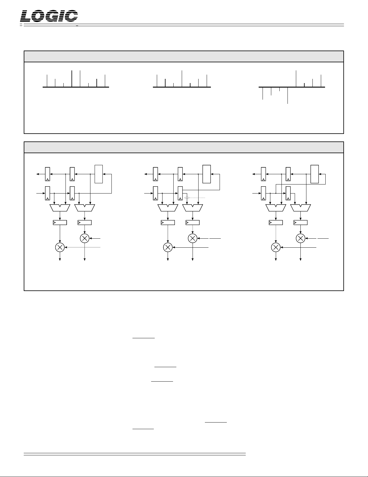
FIGURE 7. 3-3, 5-5, AND 7-7 ORTHOGONAL KERNELS
V
1
V
V
1
H
HV
2
H
1
H
3
V
3
1
The HV Filter can handle kernel sizes
of 3-3, 5-5, and 7-7 (see Figure 7).
Data delay elements at the input of
the horizontal filter and the output of
the vertical filter are used to properly
align data so that the orthogonal
kernel is implemented correctly. The
data delays are automatically set to
the correct lengths based on the
programmed length of the line buffers
and the kernel size.
Kernel sizes of 3-3, 5-5, and 7-7
require that the horizontal filter’s
output be delayed by LB – 2, 2(LB) – 3,
and 3(LB) – 4 clock cycles respectively
before being added to the vertical
filter’s output (LB is the programmed
2
H
2
H
HV
3
H
2
H
4
H
5
V
4
V
5
1
line buffer length). The data delay at
the input of the horizontal filter
handles the LB, 2(LB), and 3(LB)
delays. The data delay at the output
of the vertical filter handles the – 2, – 3,
and – 4 delays. For example, if the line
buffers are programmed for a length of
720 and a 5–5 kernel is selected, the
horizontal filter input data delay will
be 1440 clock cycles and the vertical
filter output data delay will be 3 clock
cycles.
It is important to note that the first 3,
5, or 7 multipliers of the horizontal
and vertical filters must be used in
Orthogonal Mode. If other multipliers are used, data from the horizontal
and vertical filters will not line up
correctly because the data delays are
calculated assuming that the first 3, 5,
or 7 multipliers are used. Also, the
ALUs in the horizontal filter should
be configured to accept data from the
forward I/D Register path into ALU
Input A and force ALU Input B to 0.
FUNCTIONAL DESCRIPTION
Horizontal Filter
The horizontal filter is designed to
filter a digital image in the horizontal
dimension. This FIR filter can be
configured to have as many as 16-taps
when symmetric coefficient sets are
used and 8-taps when asymmetric
coefficient sets are used.
11-0
ALUs
The ALUs double the number of filter
taps available, when symmetric
V
1
V
2
V
3
HV
4
H
3
H
5
H
6
H
7
coefficient sets are used, by
pre-adding data values which are
then multiplied by a common coefficient (see Figure 8). The ALUs can
perform two operations: A+B and
B–A. Bit 0 of Configuration Register 0 determines the ALU operation.
V
5
V
6
V
7
A+B is used with even-symmetric
coefficient sets. B–A is used with
odd-symmetric coefficient sets. Also,
either the A or B operand may be set
to 0. Bits 1 and 2 of Configuration
Register 0 control the ALU inputs.
A+0 or B+0 are used with asymmetric
coefficient sets.
Interleave/Decimation Registers
The Interleave/Decimation Registers
(I/D Registers) feed the ALU inputs.
They allow the device to filter up to
sixteen data sets interleaved into the
same data stream without having to
separate the data sets. The I/D
Registers should be set to a length
equal to the number of data sets
interleaved together. For example, if
two data sets are interleaved together,
the I/D Registers should be set to a
length of two. Bits 1 through 4 of
Configuration Register 1 determine
Video Imaging Products
6
11/08/2001-LDS.3310-H
Page 7
DEVICES INCORPORATED
FIGURE 8. SYMMETRIC COEFFICIENT SET EXAMPLES
12345678
LF3310
Horizontal / Vertical Digital Image Filter
5678
1234567
1234
Even-Tap, Even-Symmetric
Coefficient Set
FIGURE 9. I/D REGISTER DATA PATHS
REVERSAL
DATA
ALU
COEF 7
COEF 6
ALU
1-16
1-16
AB
1-16
1-16
AB
EVEN-TAP MODE ODD-TAP MODE ODD-TAP INTERLEAVE MODE
Odd-Tap, Even-Symmetric
Coefficient Set
REVERSAL
1-16
1-16
AB
ALU
1-16
1-16
AB
ALU
DATA
Delay Stage N–1
Delay Stage N
COEF 7
COEF 6
Even-Tap, Odd-Symmetric
Coefficient Set
REVERSAL
ALU
DATA
COEF 7
COEF 6
2
1-16
1-16
2
1-16
AB
ALU
1-16
AB
the I/D Register length.
The I/D Registers also facilitate using
decimation to increase the number of
filter taps. Decimation by N is
accomplished by reading the horizontal filter’s output once every N clock
cycles. The device supports decimation up to 16:1. With no decimation,
the maximum number of filter taps is
sixteen. When decimating by N, the
number of filter taps becomes 16N
because there are N–1 clock cycles
when the horizontal filter’s output is
not being read. The extra clock cycles
are used to calculate more filter taps.
When decimating, the I/D Registers
should be set to a length equal to the
decimation factor. For example,
when performing a 4:1 decimation,
the I/D Registers should be set to a
length of four. When not decimating
or when only one data set
(non-interleaved data) is fed into the
device, the I/D Registers should be
set to a length of one.
HSHEN enables or disables the
loading of data into the forward and
reverse I/D Registers when the device
is in Dimensionally Separate Mode
(see the HSHEN section for a full
discussion). When in Orthogonal
Mode, HSHEN also enables or
disables the loading of data into the
input register (DIN11-0) and the line
buffers.
It is important to note that in
Orthogonal Mode, either HSHEN or
VSHEN can disable the loading of
data into the input register (DIN11-0),
7
I/D Registers, and line buffers. Both
must be active to enable data loading
in Orthogonal Mode.
I/D Register Data Path Control
The multiplexer in the middle of the
I/D Register data path controls how
data is fed to the reverse data path.
The forward data path contains
the I/D Registers in which data
flows from left to right in the
block diagram in Figure 1. The
reverse data path contains the I/D
Registers in which data flows from
right to left. When the filter is
configured for an even number of
taps, data from the last I/D Register in the forward data path is fed
into the first I/D Register in the
reverse data path (see Figure 9).
Video Imaging Products
11/08/2001-LDS.3310-H
Page 8

DEVICES INCORPORATED
LF3310
Horizontal / Vertical Digital Image Filter
FIGURE 10. DATA REVERSAL
TXFR
LIFO A
LIFO B
1-16
When the filter is configured for an
odd number of taps, the data which
will appear at the output of the last
I/D Register in the forward data path
on the next clock cycle is fed into the
first I/D Register in the reverse data
path. Bit 5 in Configuration Register
1 configures the filter for an even or
odd number of taps.
Data Reversal
Data reversal circuitry is placed after
the multiplexer which routes data
from the forward data path to the
reverse data path (see Figure 10).
When decimating, the data stream
must be reversed in order for data to
be properly aligned at the inputs of
the ALUs. When data reversal is
enabled, the circuitry uses a pair of
LIFOs to reverse the order of the data
sent to the reverse data path. When
TXFR goes LOW, the LIFO sending
data to the reverse data path becomes
the LIFO receiving data from the
forward data path, and the LIFO
receiving data from the forward data
path becomes the LIFO sending data
to the reverse data path. The device
must see a HIGH to LOW transition
of TXFR in order to switch LIFOs. If
decimating by N, TXFR should go low
once every N clock cycles. When data
reversal is disabled, the circuitry
functions like an I/D Register. When
feeding interleaved data through the
filter, data reversal should be
disabled. Bit 6 of Configuration
Register 1 enables or disables data
reversal.
Horizontal Rounding
The horizontal filter output may be
rounded by adding the contents of
one of the sixteen horizontal round
registers to the horizontal filter output
FIGURE 11. HORIZONTAL AND VERTICAL ROUND/SELECT/LIMIT CIRCUITRY
VRSL
4
3-0
DATA IN
32
DATA IN
32
HRSL
4
3-0
When interleaved data is fed through
the device and an even tap filter is
desired, the filter should be configured for an even number of taps (Bit 5
of CR1 set to “0”) and the I/D Register length should match the number
of data sets interleaved together.
When interleaved data is to be fed
through the device and an odd tap
filter is desired, the filter should be
set to Odd-Tap Interleave Mode. Bit 0
of Configuration Register 1 configures
the filter for Odd-Tap Interleave
Mode. When the filter is configured
for Odd-Tap Interleave Mode, data
from the next to last I/D Register in
the forward data path is fed into the
first I/D Register in the reverse data
path.
When the filter is configured for an
odd number of taps (interleaved or
non-interleaved modes), the filter is
structured such that the center data
value is aligned simultaneously at the
A and B inputs of the last ALU in the
forward data path. In order to
achieve the correct result, the user
must divide the coefficient by two.
RV0RV15
32
RND
32
SV0SV15
5
SELECT
12 12
LV0LV15
24
LIMIT
VERTICAL RSL HORIZONTAL RSL
12
DATA OUT DATA OUT
RND
32
SELECT
LIMIT
12
32
5
24
RH0RH15
SH0SH15
LH0LH15
Video Imaging Products
8
11/08/2001-LDS.3310-H
Page 9

DEVICES INCORPORATED
LF3310
Horizontal / Vertical Digital Image Filter
TABLE 2. CONFIGURATION REGISTER 0 – ADDRESS 200H
BITS FUNCTION DESCRIPTION
0 ALU Mode 0 : A + B
1: B – A
1 Pass A 0: ALU Input A = 0
1: ALU Input A = Forward Register Path
2 Pass B 0: ALU Input B = 0
1: ALU Input B = Reverse Register Path
11-3 Reserved Must be set to “0”
TABLE 3. CONFIGURATION REGISTER 1 – ADDRESS 201H
BITS FUNCTION DESCRIPTION
0 Odd-Tap Interleave Mode 0 : Odd-Tap Interleave Mode Disabled
1: Odd-Tap Interleave Mode Enabled
4-1 I/D Register Length 0000: 1 Register
0001: 2 Registers
0010: 3 Registers
0011: 4 Registers
0100: 5 Registers
0101: 6 Registers
0110: 7 Registers
0111: 8 Registers
1000: 9 Registers
1001: 10 Registers
1010: 11 Registers
1011: 12 Registers
1100: 13 Registers
1101: 14 Registers
1110: 15 Registers
1111: 16 Registers
5 Horizontal Tap Number 0 : Even Number of Taps
1: Odd Number of Taps
6 Horizontal Data Reversal 0 : Data Reversal Enabled
1: Data Reversal Disabled
11-7 Reserved Must be set to “0”
(see Figure 11). Each round register is
32-bits wide and user-programmable.
This allows the filter’s output to be
rounded to any precision required.
Since any 32-bit value may be
programmed into the round registers,
the device can support complex
rounding algorithms as well as
standard Half-LSB rounding. HRSL3-
0 determines which of the sixteen
horizontal round registers are used in
the rounding operation. A value of 0
on HRSL3-0 selects horizontal round
register 0. A value of 1 selects horizontal round register 1 and so on.
HRSL3-0 may be changed every clock
cycle if desired. This allows the
rounding algorithm to be changed
every clock cycle. This is useful when
filtering interleaved data. If rounding
is not desired, a round register should
be loaded with 0 and selected as the
register used for rounding. Round
register loading is discussed in the LF
InterfaceTM section.
Horizontal Select
The word width of the horizontal
filter output is 32-bits. However, only
12-bits may be sent to the filter
output. The horizontal filter select
circuitry determines which 12-bits are
passed (see Table 1). The horizontal
select registers control the horizontal
select circuitry. There are sixteen
horizontal select registers. Each select
register is 5-bits wide and userprogrammable. HRSL3-0 determines
which of the sixteen horizontal select
registers are used in the horizontal
select circuitry. A value of 0 on
HRSL3-0 selects horizontal select
register 0. A value of 1 selects horizontal select register 1 and so on.
HRSL3-0 may be changed every clock
cycle if desired. This allows the 12-bit
window to be changed every clock
cycle. This is useful when filtering
interleaved data. Select register
loading is discussed in the LF
InterfaceTM section.
Horizontal Limiting
An output limiting function is
provided for the output of the
horizontal filter. The horizontal limit
registers determine the valid range of
output values when limiting is
enabled (Bit 1 in Configuration
Register 5). There are sixteen 24-bit
horizontal limit registers. HRSL3-0
determines which horizontal limit
register is used during the limit
operation. A value of 0 on HRSL3-0
selects horizontal limit register 0. A
value of 1 selects horizontal limit
register 1 and so on. Each limit
register contains both an upper and
lower limit value. If the value fed to
the limiting circuitry is less than the
lower limit, the lower limit value is
passed as the filter output. If the
value fed to the limiting circuitry is
greater than the upper limit, the
upper limit value is passed as the
filter output. HRSL3-0 may be
changed every clock cycle if desired.
This allows the limit range to be
Video Imaging Products
9
11/08/2001-LDS.3310-H
Page 10

DEVICES INCORPORATED
LF3310
Horizontal / Vertical Digital Image Filter
changed every clock cycle. This is
useful when filtering interleaved
data. When loading limit values into
the device, the upper limit must be
greater than the lower limit. Limit
register loading is discussed in the LF
InterfaceTM section.
Vertical Filter
The vertical filter is designed to filter
a digital image in the vertical dimension. It is a FIR filter which can be
configured to have as many as 8-taps.
Line Buffers
There are seven on-chip line buffers.
The maximum delay length of each
line buffer is 3076 cycles and the
minimum is 4 cycles. Configuration
Register 2 (CR2) determines the delay
length of the line buffers. The line
buffer length is equal to the value of
CR2 plus 4. A value of 0 for CR2 sets
the line buffer length to 4. A value of
3072 for CR2 sets the line buffer
length to 3076. Any values for CR2
greater than 3072 are not valid.
section for a full discussion). When in
Orthogonal Mode, VSHEN also
enables or disables the loading of data
into the input register (DIN11-0) and
the forward and reverse I/D Registers.
It is important to note that in Orthogonal Mode, either HSHEN or
VSHEN can disable the loading of
data into the input register (DIN11-0),
I/D Registers, and line buffers. Both
Interleaved Data
The vertical filter is capable of
handling interleaved data. The
number of data sets it can handle is
determined by the number of data
values contained in a video line. If
the interleaved video line has 3076
data values or less, the vertical filter
can handle it no matter how many
data sets are interleaved together.
must be active to enable data loading
in Orthogonal Mode.
TABLE 4. CONFIGURATION REGISTER 2 – ADDRESS 202H
BITS FUNCTION DESCRIPTION
11-0 Line Buffer Length See Line Buffer Description Section
TABLE 5. CONFIGURATION REGISTER 3 – ADDRESS 203H
BITS FUNCTION DESCRIPTION
0 Line Buffer Mode 0 : Delay Mode
1: Recirculate Mode
1 Line Buffer Load 0 : Normal Load
1: Parallel Load
11-2 Reserved Must be set to “0”
The line buffers have two modes of
operation: delay mode and recirculate
mode. Bit 0 of Configuration Register
3 determines which mode the line
buffers are in. In delay mode, the
data input to the line buffer is delayed
by an amount determined by CR2. In
recirculate mode, the output of the
line buffer is routed back to the input
of the line buffer allowing the line
buffer contents to be read multiple
times.
Bit 1 of Configuration Register 3
allows the line buffers to be loaded in
parallel. When Bit 1 is “1”, the input
register (DIN11-0) loads all seven line
buffers in parallel. This allows all the
line buffers to be preloaded with data
in the amount of time it normally
takes to load a single line buffer.
VSHEN enables or disables the
loading of data into the line buffers
when the device is in Dimensionally
Separate Mode (see the VSHEN
TABLE 6. CONFIGURATION REGISTER 4 – ADDRESS 204H
BITS FUNCTION DESCRIPTION
0 HV Filter Mode 0: Orthogonal Mode
1: Dimensionally Separate
1 HV Direction 0: Horizontal to Vertical
1: Vertical to Horizontal
3-2 Orthogonal Kernel Size 00: 3-3 Kernel
01: 5-5 Kernel
10: 7-7 Kernel
11: Not Used
4 Limit Register Load Control 0 : Limit Registers Always Enabled
1 : Limit Registers Under Shift Enable Control
11-5 Reserved Must be set to “0”
TABLE 7. CONFIGURATION REGISTER 5 – ADDRESS 205H
BITS FUNCTION DESCRIPTION
0 Vertical Limit Enable 0 : Vertical Limiting Disabled
1: Vertical Limiting Enabled
1 Horizontal Limit Enable 0 : Horizontal Limiting Disabled
1: Horizontal Limiting Enabled
11-2 Reserved Must be set to “0”
Video Imaging Products
10
11/08/2001-LDS.3310-H
Page 11

DEVICES INCORPORATED
LF3310
Horizontal / Vertical Digital Image Filter
TABLE 8. HCF/VCF11-9 DECODE
11 10 9 DESCRIPTION
0 0 0 Coefficient Banks
0 0 1 Configuration Registers
0 1 0 Horizontal Select Registers
0 1 1 Vertical Select Registers
1 0 0 Horizontal Round Registers
1 0 1 Vertical Round Registers
1 1 0 Horizontal Limit Registers
1 1 1 Vertical Limit Registers
Vertical Rounding
The vertical filter output may be
rounded by adding the contents of
one of the sixteen vertical round
registers to the vertical filter output
(see Figure 11). Each round register is
32-bits wide and user-programmable.
This allows the filter’s output to be
rounded to any precision required.
Since any 32-bit value may be
programmed into the round registers,
the device can support complex
rounding algorithms as well as
standard Half-LSB rounding.
VRSL3-0 determines which of the
sixteen vertical round registers are
used in the rounding operation. A
value of 0 on VRSL3-0 selects vertical
round register 0. A value of 1 selects
vertical round register 1 and so on.
VRSL3-0 may be changed every clock
cycle if desired. This allows the
rounding algorithm to be changed
every clock cycle. This is useful when
filtering interleaved data. If rounding
is not desired, a round register should
be loaded with 0 and selected as the
register used for rounding. Round
register loading is discussed in the LF
InterfaceTM section.
Vertical Select
The word width of the vertical filter
output is 32-bits. However, only
12-bits may be sent to the filter
output. The vertical filter select
circuitry determines which 12-bits are
passed (see Table 1). The vertical
select registers control the vertical
select circuitry. There are sixteen
vertical select registers. Each select
TABLE 9. HRZ. ROUND REGISTERS
REGISTER ADDRESS (HEX)
0 800
1 801
14 80E
15 80F
TABLE 10. HRZ. SELECT REGISTERS
REGISTER ADDRESS (HEX)
0 400
1 401
14 40E
15 40F
TABLE 11. HRZ. LIMIT REGISTERS
REGISTER ADDRESS (HEX)
0 C00
1 C01
14 C0E
15 C0F
register is 5-bits wide and
user-programmable. VRSL3-0 determines which of the sixteen vertical
select registers are used in the vertical
select circuitry. A value of 0 on
VRSL3-0 selects vertical select register
0. A value of 1 selects vertical select
register 1 and so on. VRSL3-0 may be
changed every clock cycle if desired.
This allows the 12-bit window to be
changed every clock cycle. This is
useful when filtering interleaved
data. Select register loading is
discussed in the LF Interface
section.
Vertical Limiting
An output limiting function is provided for the output of the vertical
filter. The vertical limit registers
determine the valid range of output
values when limiting is enabled (Bit 0
in Configuration Register 5). There
TM
TABLE 12. VRT. ROUND REGISTERS
REGISTER ADDRESS (HEX)
0 A00
1 A01
14 A0E
15 A0F
TABLE 13. VRT. SELECT REGISTERS
REGISTER ADDRESS (HEX)
0 600
1 601
14 60E
15 60F
TABLE 14. VRT. LIMIT REGISTERS
REGISTER ADDRESS (HEX)
0 E00
1 E01
14 E0E
15 E0F
are sixteen 24-bit vertical limit
registers. VRSL3-0 determines which
vertical limit register is used during
the limit operation. A value of 0 on
VRSL3-0 selects vertical limit register
0. A value of 1 selects vertical limit
register 1 and so on. Each limit
register contains both an upper and
lower limit value. If the value fed to
the limiting circuitry is less than the
lower limit, the lower limit value is
passed as the filter output. If the
value fed to the limiting circuitry is
greater than the upper limit, the upper
limit value is passed as the filter output.
VRSL3-0 may be changed every clock
cycle if desired. This allows the limit
range to be changed every clock cycle.
This is useful when filtering interleaved
data. When loading limit values into
the device, the upper limit must be
greater than the lower limit. Limit
register loading is discussed in the LF
InterfaceTM section.
Video Imaging Products
11
11/08/2001-LDS.3310-H
Page 12

DEVICES INCORPORATED
FIGURE 12. COEFFICIENT BANK LOADING SEQUENCE
COEFFICIENT SET 1 COEFFICIENT SET 2 COEFFICIENT SET 3
CLK
HLD/VLD
W1
LF3310
Horizontal / Vertical Digital Image Filter
W2 W3
HCF/VCF
11-0
W1: Coefficient Set 1 written to coefficient banks during this clock cycle.
W2: Coefficient Set 2 written to coefficient banks during this clock cycle.
W3: Coefficient Set 3 written to coefficient banks during this clock cycle.
ADDR1 COEF0 COEF7 ADDR2 COEF0 COEF7 ADDR3 COEF0 COEF7
FIGURE 13. CONFIGURATION/CONTROL REGISTER LOADING SEQUENCE
CONFIG REG ROUND REGISTER LIMIT REGISTER
CLK
HLD/VLD
HCF/VCF
11-0
W1: Configuration Register loaded with new data on this rising clock edge.
W2: Select Register loaded with new data on this rising clock edge.
W3: Round Register loaded with new data on this rising clock edge.
W4: Limit Register loaded with new data on this rising clock edge.
ADDR1DATA
Coefficient Banks
The coefficient banks store the
coefficients which feed into the
multipliers in the horizontal and
vertical filters. There is a separate
bank for each multiplier. Each bank
can hold 256 12-bit coefficients. The
banks are loaded using an LF
InterfaceTM. There is a separate LF
InterfaceTM for the horizontal and
vertical banks. Coefficient bank
loading is discussed in the LF
InterfaceTM section.
Configuration and Control Registers
The Configuration Registers determine how the HV Filter operates.
Tables 2 through 7 show the formats
of the six configuration registers.
There are three types of control
registers: round, select, and limit.
There are sixteen round registers for
SELECT REG
W1
ADDR
1
W2
ADDR
3
2
DATA
1
DATA
1
DATA
DATA
2
the horizontal filter and sixteen for the
vertical filter. Each register is 32-bits
wide. HRSL3-0 and VRSL3-0 determine
which horizontal and vertical round
registers respectively are used for
rounding.
There are sixteen select registers for
the horizontal filter and sixteen for
the vertical filter. Each register is
5-bits wide. HRSL3-0 and VRSL3-0
determine which horizontal and
vertical select registers respectively
are used in the select circuitry.
There are sixteen limit registers for
the horizontal filter and sixteen for
the vertical filter. Each register is
24-bits wide and stores both an upper
and lower limit value. The lower
limit is stored in bits 11-0 and the
upper limit is stored in bits 23-12.
HRSL3-0 and VRSL3-0 determine
which horizontal and vertical limit
registers respectively are used for
W3 W4
DATA
4
3
ADDR
4
DATA
DATA
2
1
limiting when limiting is enabled.
Configuration and Control Register
loading is discussed in the LF
InterfaceTM section.
LF Interface
TM
The Horizontal and Vertical
LF InterfacesTM are used to load data
into the horizontal and vertical
coefficient banks respectively. They
are also used to load data into the
Configuration and Control Registers.
The following section describes how
the Horizontal LF InterfaceTM works.
The Horizontal and Vertical
LF InterfacesTM are identical in
function. If HLD and HCF11-0 are
replaced with VLD and VCF11-0, the
following section will describe how
the Vertical LF InterfaceTM works.
HLD is used to enable and disable the
Horizontal LF InterfaceTM. When
Video Imaging Products
12
11/08/2001-LDS.3310-H
Page 13

DEVICES INCORPORATED
LF3310
Horizontal / Vertical Digital Image Filter
HLD goes LOW, the Horizontal LF
InterfaceTM is enabled for data input.
The first value fed into the interface
on HCF11-0 is an address which
determines what the interface is going
to load. The three most significant
bits (HCF11-9) determine if the LF
InterfaceTM will load coefficient banks
or Configuration/Control Registers
(see Table 8). The nine least significant bits (HCF8-0) are the address for
whatever is to be loaded (see
Tables 9-14). For example, to load
address 15 of the horizontal coefficient
banks, the first data value into the
LF InterfaceTM should be 00FH. To
load horizontal limit register 10, the
first data value should be C0AH. Th e
first address value should be loaded into
the interface on the same clock cycle that
latches the HIGH to LOW transition of
HLD (see Figures 12 and 13).
The next value(s) loaded into the
interface are the data value(s) which
will be stored in the bank or register
defined by the address value. When
loading coefficient banks, the interface will expect eight values to be
loaded into the device after the
address value. The eight values are
coefficients 0 through 7. When
loading select or Configuration
Registers, the interface will expect one
value after the address value. When
loading round registers, the interface
will expect four values after the
address value. When loading limit
registers, the interface will expect two
values after the address value.
Figures 12 and 13 show the data
loading sequences for the coefficient
banks and Configuration/Control
Registers.
Both HPAUSE and VPAUSE allow the
user to effectively slow the rate of data
loading through the LF InterfaceTM.
When HPAUSE is HIGH, the LF
InterfaceTM affecting the data used for
the Horizontal Filter is held until
HPAUSE is returned to a LOW.
When VPAUSE is HIGH, the LF
InterfaceTM affecting the data used for
the Vertical Filter is held until
VPAUSE is returned to a LOW.
Figures 14 through 17 display the
effects of both HPAUSE and VPAUSE
while loading coefficient and control
data.
Table 15 shows an example of loading
data into the coefficient banks. The
following data values are written into
address 10 of coefficient banks 0
through 7: 210H, 543H, C76H, 9E3H,
701H, 832H, F20H, 143H. Table 16
FIGURE 14. COEFFICIENT BANK LOADING SEQUENCE WITH HPAUSE AND VPAUSE IMPLEMENTATION
COEFFICIENT SET 1
CLK
W1
HPAUSE/VPAUSE
HLD/VLD
HCF/VCF
11-0
W1: Coefficient Set 1 written to coefficient banks during this clock cycle.
ADDR1 COEF0 COEF1
COEF7
FIGURE 15. CONFIGURATION AND SELECT REGISTER LOADING SEQUENCE WITH HPAUSE AND VPAUSE IMPLEMENTATION
CLK
HPAUSE/VPAUSE
HLD/VLD
11-0
HCF/VCF
CONFIGURATION REGISTER
ADDR
1
DATA
W1
1
ADDR
SELECT REGISTER
2
DATA
W2
1
W1: Configuration Register loaded with new data on this rising clock edge.
W2: Select Register loaded with new data on this rising clock edge.
13
Video Imaging Products
11/08/2001-LDS.3310-H
Page 14

DEVICES INCORPORATED
LF3310
Horizontal / Vertical Digital Image Filter
shows an example of loading data
into a Configuration Register. Data
value 003H is written into Configuration Register 4. Table 17 shows an
example of loading data into a round
register. Data value 7683F4A2H is
written into horizontal round register
12. Table 18 shows an example of
loading data into a select register.
Data value 00FH is loaded into
horizontal select register 2. Table 19
shows an example of loading data
into vertical limit register 7. Data
value 390H is loaded as the lower
limit and 743H is loaded as the upper
limit.
FIGURE 16. ROUND REGISTER LOADING SEQUENCE WITH HPAUSE AND VPAUSE IMPLEMENTATION
ROUND REGISTER
CLK
HPAUSE/VPAUSE
HLD/VLD
HCF/VCF
11-0
W1: Round Register loaded with new data on this rising clock edge.
ADDR
1
DATA
1
DATA
2
DATA
3
DATA
FIGURE 17. LIMIT REGISTER LOADING SEQUENCE WITH HPAUSE AND VPAUSE IMPLEMENTATION
W1
4
LIMIT REGISTER
CLK
W1
HPAUSE/VPAUSE
HLD/VLD
HCF/VCF
11-0
W1: Limit Register loaded with new data on this rising clock edge.
ADDR
1
DATA
1
DATA
2
TABLE 15. COEFFICIENT BANK LOADING FORMAT
H/VCF11 H/VCF10 H/VCF9 H/VCF8 H/VCF7 H/VCF6 H/VCF5 H/VCF4 H/VCF3 H/VCF2 H/VCF1 H/VCF0
1st Word - Address 0 0 0000001010
2nd Word - Bank 0 0 0 1000010000
3rd Word - Bank 1 0 1 0101000011
4th Word - Bank 2 1 1 0001110110
5th Word - Bank 3 1 0 0111100011
6th Word - Bank 4 0 1 1100000001
7th Word - Bank 5 1 0 0000110010
8th Word - Bank 6 1 1 1100100000
9th Word - Bank 7 0 0 0101000011
Video Imaging Products
14
11/08/2001-LDS.3310-H
Page 15

DEVICES INCORPORATED
LF3310
Horizontal / Vertical Digital Image Filter
It takes 9S clock cycles to load S
coefficient sets into the device.
Therefore, it takes 2304 clock cycles to
load all 256 coefficient sets. Assuming
an 83 MHz clock rate, all 256 coefficient sets can be updated in 28.8 µs,
which is well within vertical blanking
time. It takes 5S or 3S clock cycles to
load S round or limit registers respectively. Therefore, it takes 256 clock
cycles to update all round and limit
registers (both horizontal and vertical). Assuming an 83 MHz clock rate,
all horizontal and vertical Round/
Limit registers can be updated in
3.08 µs.
The coefficient banks and Configura-
tion/Control Registers are not loaded
with data until all data values for the
specified address are loaded into the
LF InterfaceTM. In other words, the
coefficient banks are not written to
until all eight coefficients have been
loaded into the LF InterfaceTM. A
round register is not written to until
all four data values are loaded.
After the last data value is loaded, the
interface will expect a new address
value on the next clock cycle. After
the next address value is loaded, data
loading will begin again as previously
discussed. As long as data is loaded
into the interface, HLD must remain
LOW. After all desired coefficient
banks and Configuration/Control
Registers are loaded with data, the LF
InterfaceTM must be disabled. This is
TABLE 16. CONFIGURATION REGISTER LOADING FORMAT
H/VCF11 H/VCF10 H/VCF9 H/VCF8 H/VCF7 H/VCF6 H/VCF5 H/VCF4 H/VCF3 H/VCF2 H/VCF1 H/VCF0
1st Word - Address 0 0 1000000100
2nd Word - Data 0 0 0000000011
TABLE 17. ROUND REGISTER LOADING FORMAT
H/VCF11 H/VCF10 H/VCF9 H/VCF8 H/VCF7 H/VCF6 H/VCF5 H/VCF4 H/VCF3 H/VCF2 H/VCF1 H/VCF0
1st Word - Address 1 0 0000001100
2nd Word- Data R RRR10100010*
3rd Word - Data R RRR11110100
4th Word - Data R RRR10000011
5th Word - Data R RRR0**1110110
R = Reserved. Must be set to “0”.
* This bit represents the LSB of the Round Register.
** This bit represents the MSB of the Round Register.
Video Imaging Products
15
11/08/2001-LDS.3310-H
Page 16

DEVICES INCORPORATED
LF3310
Horizontal / Vertical Digital Image Filter
done by setting HLD HIGH on the
clock cycle after the clock cycle which
latches the last data value. It is
important that the LF Interface
TM
remain disabled when not loading
data into it.
The horizontal coefficient banks may
only be loaded with the Horizontal
LF InterfaceTM and the vertical coefficient banks may only be loaded with
the Vertical LF InterfaceTM. The
Configuration and Control Registers
may be loaded with either the Hori-
zontal or Vertical LF InterfacesTM.
Since both LF InterfacesTM operate
independently of each other, both
LF InterfacesTM can load data into
their respective coefficient banks at
the same time. Or, one LF Interface
TM
can load the Configuration/Control
Registers while the other loads it’s
respective coefficient banks. If both
LF InterfacesTM are used to load a
configuration or control register at the
same time, the Vertical LF Interface
TM
will be given priority over the Hori-
zontal LF InterfaceTM. For example, if
the Horizontal LF InterfaceTM at-
tempts to load data into a Configura-
tion Register at the same time that the
Vertical LF InterfaceTM attempts to
load a horizontal round register, the
Vertical LF InterfaceTM will be allowed
to load the round register while the
Horizontal LF InterfaceTM will not be
allowed to load the Configuration
Register. However, the Horizontal
LF InterfaceTM will continue to func-
tion as if the write occurred.
TABLE 18. SELECT REGISTER LOADING FORMAT
H/VCF11 H/VCF10 H/VCF9 H/VCF8 H/VCF7 H/VCF6 H/VCF5 H/VCF4 H/VCF3 H/VCF2 H/VCF1 H/VCF0
1st Word - Address 0 1 0000000010
2nd Word - Data 0 0 0000001111
TABLE 19. LIMIT REGISTER LOADING FORMAT
H/VCF11 H/VCF10 H/VCF9 H/VCF8 H/VCF7 H/VCF6 H/VCF5 H/VCF4 H/VCF3 H/VCF2 H/VCF1 H/VCF0
1st Word - Address 1 1 1000000111
2nd Word- Data 0* 0 1110010000
3rd Word - Data 0**1 1101000011
* This bit represents the MSB of the Lower Limit.
** This bit represents the MSB of the Upper Limit.
Video Imaging Products
16
11/08/2001-LDS.3310-H
Page 17

DEVICES INCORPORATED
LF3310
Horizontal / Vertical Digital Image Filter
MAXIMUM RATINGS
Storage temperature ........................................................................................................... –65°C to +150°C
Operating ambient temperature........................................................................................... –55°C to +125°C
VCC supply voltage with respect to ground............................................................................ –0.5 V to +4.5V
Input signal with respect to ground .......................................................................................... –0.5 V to 5.5 V
Signal applied to high impedance output ................................................................................. –0.5 V to 5.5 V
Output current into low outputs............................................................................................................. 25 mA
Latchup current ............................................................................................................................... > 400 mA
ESD Classification (MIL-STD-883E METHOD 3015.7) ...................................................................... Class 3
OPERATING CONDITIONS
Active Operation, Commercial 0ºC to +70ºC 3.00 V ≤ VCC ≤ 3.60 V
Active Operation, Military –55ºC to +125ºC 3.00 V ≤ VCC ≤ 3.60 V
Above which useful life may be impaired (Notes 1, 2, 3, 8)
To meet specified electrical and switching characteristics
Mode Temperature Range (Ambient) Supply Voltage
ELECTRICAL CHARACTERISTICS
Symbol Parameter Test Condition Min Typ Max Unit
VOH Output High Voltage VCC = Min., IOH = –4 mA 2.4 V
VOL Output Low Voltage VCC = Min., IOL = 8.0 mA 0.4 V
VIH Input High Voltage 2.0 5.5 V
VIL Input Low Voltage (Note 3) 0.0 0.8 V
IIX Input Current Ground ≤ VIN ≤ VCC (Note 12) ±10 µA
IOZ Output Leakage Current Ground ≤ VOUT ≤ VCC (Note 12) ±10 µA
ICC1 VCC Current, Dynamic (Notes 5, 6) 250 mA
ICC2 VCC Current, Quiescent (Note 7) 2mA
CIN Input Capacitance TA = 25°C, f = 1 MHz 1 0 pF
COUT Output Capacitance TA = 25°C, f = 1 MHz 10 pF
Over Operating Conditions (Note 4)
Video Imaging Products
17
11/08/2001-LDS.3310-H
Page 18

DEVICES INCORPORATED
9
9
9
9
9
9
9
9
9
9
9
9
9
9
9
9
9
9
9
9
9
9
9
9
9
9
9
9
9
9
9
9
9
9
9
9
4
4
SWITCHING CHARACTERISTICS
LF3310
Horizontal / Vertical Digital Image Filter
COMMERCIAL OPERATING RANGE (0°C to +70°C)
Symbol Parameter Min Max Min Max Min Max Min Max
tCYC Cycle Time 25 18 15 12
tPWL Clock Pulse Width Low 1 0 8 7 5
tPWH Clock Pulse Width High 10 8 7 5
tS0 Input Setup Time 8654
tS1 Input Setup Time (xCEN, xRSL)* 8654
tH0 Input Hold Time 1111
tH1 Input Hold Time (xCEN, xRSL)* 1. 5 1. 5 1.5 1. 5
tD Output Delay 13 11 10 8
tDIS Three-State Output Disable Delay (Note 11) 15 13 12 10
tENA Three-State Output Enable Delay (Note 11) 15 13 12 10
Notes 9, 10 (ns)
234567890123456789012345678
234567890123456789012345678
234567890123456789012345678
234567890123456789012345678
234567890123456789012345678
234567890123456789012345678
234567890123456789012345678
234567890123456789012345678
234567890123456789012345678
234567890123456789012345678
234567890123456789012345678
234567890123456789012345678
234567890123456789012345678
234567890123456789012345678
234567890123456789012345678
234567890123456789012345678
234567890123456789012345678
234567890123456789012345678
234567890123456789012345678
234567890123456789012345678
234567890123456789012345678
234567890123456789012345678
234567890123456789012345678
234567890123456789012345678
234567890123456789012345678
234567890123456789012345678
234567890123456789012345678
234567890123456789012345678
234567890123456789012345678
234567890123456789012345678
234567890123456789012345678
234567890123456789012345678
234567890123456789012345678
234567890123456789012345678
234567890123456789012345678
234567890123456789012345678
25
*
18
LF3310–
*
15 12
SWITCHING WAVEFORMS:DATA I/O
CLK
DIN
11-0
HCA
VCA
CONTROLS
(Except OE)
xCEN, xRSL
123456
t
H0
t
S0
DIN
N
7-0
7-0
HCA/VCA
t
S1
N
t
H1
DIN
HCA/VCA
N+1
N+1
t
PWH
t
CYC
t
PWL
7
OE
t
ENA
DOUT
15-0
t
DIS
HIGH IMPEDANCE
* The ‘x’ represents both horizontal and vertical signals for each case.
2345678901234567890123
2345678901234567890123
*DISCONTINUED SPEED GRADE
18
t
D
OUTPUTN-
1
OUTPUT
N
Video Imaging Products
11/08/2001-LDS.3310-H
Page 19

DEVICES INCORPORATED
9
9
9
9
9
9
9
9
9
9
9
9
9
9
9
9
9
9
9
9
9
9
9
9
4
4
LF3310
Horizontal / Vertical Digital Image Filter
COMMERCIAL OPERATING RANGE (0°C to +70°C)
Symbol Parameter Min Max Min Max Min Max Min Max
tCFS Coefficient Input Setup Time 8655
tCFH Coefficient Input Hold Time 1 1 1 1.5
tLS Load Setup Time 8654
tLH Load Hold Time 1 1 1 1.5
tPS PAUSE Setup Time 8654
tPH PAUSE Hold Time 1 .5 1.5 1.5 1.5
SWITCHING WAVEFORMS: LF INTERFACE
12 453
TM
Notes 9, 10 (ns)
234567890123456789012345678
234567890123456789012345678
234567890123456789012345678
234567890123456789012345678
234567890123456789012345678
234567890123456789012345678
234567890123456789012345678
234567890123456789012345678
234567890123456789012345678
234567890123456789012345678
234567890123456789012345678
234567890123456789012345678
234567890123456789012345678
234567890123456789012345678
234567890123456789012345678
234567890123456789012345678
234567890123456789012345678
234567890123456789012345678
234567890123456789012345678
234567890123456789012345678
234567890123456789012345678
234567890123456789012345678
234567890123456789012345678
234567890123456789012345678
25
*
18
LF3310–
*
15 12
6
CLK
t
HLD
VLD
HPAUSE
VPAUSE
HCF
11–0
VCF
11–0
t
LS
t
CFS
ADDRESS
t
CFH
t
PWH
t
CYC
CF
t
PWL
t
PS
0
t
PH
LH
CF
1
CF
2
2345678901234567890123
2345678901234567890123
*DISCONTINUED SPEED GRADE
Video Imaging Products
19
11/08/2001-LDS.3310-H
Page 20

DEVICES INCORPORATED
NOTES
LF3310
Horizontal / Vertical Digital Image Filter
1. Maximum Ratings indicate stress
specifications only. Functional operation of these products at values beyond
those indicated in the Operating Conditions table is not implied. Exposure to
maximum rating conditions for extended periods may affect reliability.
2. The products described by this specification include internal circuitry designed to protect the chip from damaging substrate injection currents and accumulations of static charge. Nevertheless, conventional precautions
should be observed during storage,
handling, and use of these circuits in
order to avoid exposure to excessive
electrical stress values.
3. This device provides hard clamping
of transient undershoot. Input levels
below ground will be clamped beginning at –0.6 V. The device can withstand indefinite operation with inputs
or outputs in the range of –0.5 V to
+5.5 V. Device operation will not be
adversely affected, however, input current levels will be well in excess of 100
mA.
4. Actual test conditions may vary from
those designated but operation is guaranteed as specified.
5. Supply current for a given application can be accurately approximated
by:
2
NCV F
4
where
N = total number of device outputs
C = capacitive load per output
V = supply voltage
F = clock frequency
6. Tested with outputs changing every
cycle and no load, at a 40 MHz clock
rate.
7. Tested with all inputs within 0.1 V of
VCC or Ground, no load.
8. These parameters are guaranteed
but not 100% tested.
9. AC specifications are tested with
input transition times less than 3 ns,
output reference levels of 1.5 V (except
tDIS test), and input levels of nominally
0 to 3.0 V. Output loading may be a
resistive divider which provides for
specified IOH and IOL at an output
voltage of VOH min and VOL max
respectively. Alternatively, a diode
bridge with upper and lower current
sources of IOH and IOL respectively,
and a balancing voltage of 1.5 V may be
used. Parasitic capacitance is 30 pF
minimum, and may be distributed.
This device has high-speed outputs capable of large instantaneous current
pulses and fast turn-on/turn-off times.
As a result, care must be exercised in the
testing of this device. The following
measures are recommended:
a. A 0.1 µF ceramic capacitor should be
installed between VCC and Ground
leads as close to the Device Under Test
(DUT) as possible. Similar capacitors
should be installed between device VCC
and the tester common, and device
ground and tester common.
b. Ground and VCC supply planes
must be brought directly to the DUT
socket or contactor fingers.
c. Input voltages on a test fixture
should be adjusted to compensate for
inductive ground and VCC noise to maintain required DUT input levels relative
to the DUT ground pin.
10. Each parameter is shown as a minimum or maximum value. Input requirements are specified from the point
of view of the external system driving
the chip. Setup time, for example, is
specified as a minimum since the external system must supply at least that
much time to meet the worst-case requirements of all parts. Responses from
the internal circuitry are specified from
the point of view of the device. Output
delay, for example, is specified as a
maximum since worst-case operation of
any device always provides data within
that time.
11. For the tENA test, the transition is
measured to the 1.5 V crossing point
with datasheet loads. For the tDIS test,
the transition is measured to the
±200mV level from the measured
steady-state output voltage with
±10mA loads. The balancing volt-
age, VTH, is set at 3.0 V for Z-to-0
and 0-to-Z tests, and set at 0 V for Z-
to-1 and 1-to-Z tests.
12. These parameters are only tested at
the high temperature extreme, which is
the worst case for leakage current.
FIGURE A. OUTPUT LOADING CIRCUIT
DUT
S1
I
OL
V
C
L
I
TH
OH
FIGURE B. THRESHOLD LEVELS
t
VOL*
V
DIS
0.2 V
0.2 V
OH
*
3.0V Vth
0
Z
Z
1
0V Vth
t
ENA
OE
1.5 V 1.5 V
Z
0
Z
1
V
OL
*
OH
*
V
Measured V
Measured V
1.5 V
1.5 V
OL
with IOH = –10mA and IOL = 10mA
OH
with IOH = –10mA and IOL = 10mA
Video Imaging Products
20
11/08/2001-LDS.3310-H
Page 21

DEVICES INCORPORATED
ORDERING INFORMATION
144-pin
VCC
GND
GND
GND
GND
VCC
GND
DIN11
DIN10
DIN9
DIN8
DIN7
DIN6
GND
VCC
DIN5
DIN4
DIN3
DIN2
DIN1
DIN0
GND
VCC
VCA7
VCA6
VCA5
VCA4
VCA3
VCA2
VCA1
VCA0
VCEN
VSHEN
VCC
VCC
VCC
Horizontal / Vertical Digital Image Filter
GND
GND
GND
GND
GND
HCF11
HCF10
HCF9
HCF8
HCF7
HCF6
HCF5
HCF4
HCF3
HCF2
HCF1
HCF0
GND
CLK
VCC
HLD
GND
VCC
HPAUSE
GND
VCC
HSHEN
GND
VCC
TXFR
144
143
142
141
140
139
138
137
136
135
134
133
132
131
130
129
128
127
126
125
124
123
122
121
120
119
118
117
116
1
2
3
4
5
6
7
8
9
10
11
12
13
14
15
16
17
18
19
20
21
22
23
24
25
26
27
28
29
30
31
32
33
34
35
36
3738394041424344454647484950515253545556575859606162636465666768697071
Top
View
115
VCC
114
GND
113
GND
112
VCC
111
VCC
110
VCC
109
108
107
106
105
104
103
102
101
100
72
LF3310
GND
GND
HCA7
HCA6
HCA5
HCA4
HCA3
HCA2
HCA1
HCA0
99
VCC
98
GND
97
HCEN
96
GND
95
VCC
94
GND
93
GND
92
GND
91
GND
90
89
88
87
86
85
84
83
82
81
80
79
78
77
76
75
74
73
11
VCF
VCF10
VCF9
VCF8
VCF7
VCF6
VCF5
VCF4
VCF3
VCF2
VCF1
VCF0
VLD
VPAUSE
VCC
VCC
VCC
Speed
15 ns
12 ns
NCNCNC
GND
GND
VACC
VCC
GND
VRSL2
VRSL1
VRSL0
VRSL3
Plastic Quad Flatpack
(Q5)
0°C to +70°C — COMMERCIAL SCREENING
LF3310QC15
LF3310QC12
–55°C to +125°C — COMMERCIAL SCREENING
–55°C to +125°C — MIL-STD-883 COMPLIANT
NC
DOUT11
OE
GND
DOUT7
DOUT9
DOUT8
DOUT6
DOUT5
DOUT4
DOUT10
DOUT3
VCC
GND
GND
DOUT2
DOUT1
HRSL3
DOUT0
GND
HACC
HRSL2
HRSL1
HRSL0
Video Imaging Products
21
11/08/2001-LDS.3310-H
 Loading...