

Page 1
August 2000
LF147/LF347
Wide Bandwidth Quad JFET Input Operational Amplifiers
LF147/LF347 Wide Bandwidth Quad JFET Input Operational Amplifiers
General Description
The LF147 is a low cost, high speed quad JFET input
operational amplifier with an internally trimmed input offset
voltage (BI-FET II
supply current and yet maintains a large gain bandwidth
product and a fast slew rate. In addition, well matched high
voltage JFET input devices provide very low input bias and
offset currents. The LF147 is pin compatible with the standard LM148. This feature allows designers to immediately
upgrade the overall performance of existing LF148 and
LM124 designs.
The LF147 may be used in applications such as high speed
integrators, fast D/A converters, sample-and-hold circuits
and many other circuits requiring low input offset voltage,
low input bias current, high input impedance, high slew rate
and wide bandwidth. The device has low noise and offset
voltage drift.
™
technology). The device requires a low
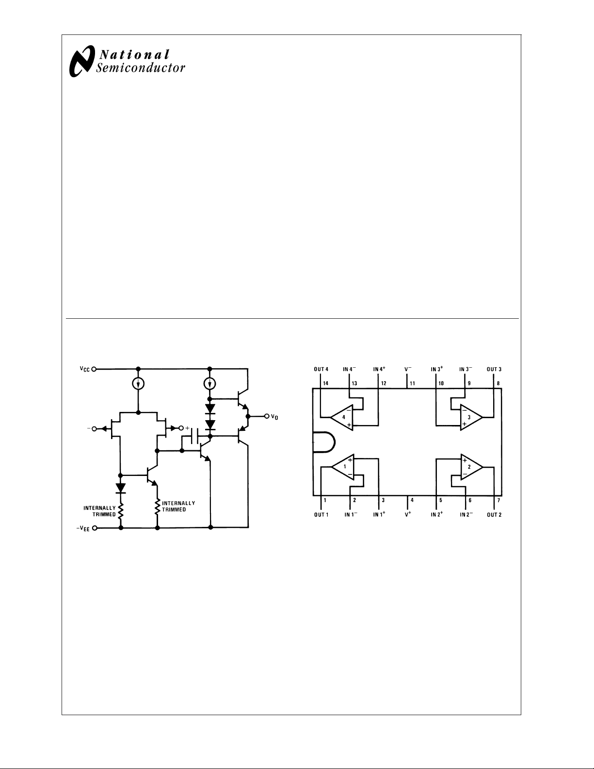
Simplified Schematic
1
⁄4Quad
Features
n Internally trimmed offset voltage: 5 mV max
n Low input bias current: 50 pA
n Low input noise current: 0.01 pA/
n Wide gain bandwidth: 4 MHz
n High slew rate: 13 V/µs
n Low supply current: 7.2 mA
n High input impedance: 10
n Low total harmonic distortion: ≤0.02%
n Low 1/f noise corner: 50 Hz
n Fast settling time to 0.01%: 2 µs
√
Hz
12
Connection Diagram
Dual-In-Line Package
Ω
00564713
BI-FET II™is a trademark of National Semiconductor Corporation.
© 2004 National Semiconductor Corporation DS005647 www.national.com
Note 1: LF147 available as per JM38510/11906.
Top View
Order Number LF147J, LF147J-SMD, LF347M,
LF347BN, LF347N, LF147J/883,
or JL147 BCA (Note 1)
See NS Package Number J14A, M14A or N14A
00564701
Page 2
Absolute Maximum Ratings (Note 2)
If Military/Aerospace specified devices are required,
please contact the National Semiconductor Sales Office/
Distributors for availability and specifications.
LF147/LF347
Supply Voltage
Differential Input Voltage
Input Voltage Range
(Note 3)
Output Short Circuit Continuous Continuous
Duration (Note 4)
Power Dissipation 900 mW 1000 mW
(Notes 5, 11)
T
max 150˚C 150˚C
j
θ
jA
Ceramic DIP (J) Package 70˚C/W
Plastic DIP (N) Package 75˚C/W
LF147 LF347B/LF347
±
22V
±
38V
±
19V
±
±
±
18V
30V
15V
Operating Temperature (Note 6) (Note 6)
Range
Storage Temperature
Range −65˚C≤T
Lead Temperature
(Soldering, 10 sec.) 260˚C 260˚C
Soldering Information
Dual-In-Line Package
Soldering (10 seconds) 260˚C
Small Outline Package
Vapor Phase (60 seconds) 215˚C
Infrared (15 seconds) 220˚C
See AN-450 “Surface Mounting Methods and Their Effect
on Product Reliability” for other methods of soldering
surface mount devices.
ESD Tolerance (Note 12) 900V
LF147 LF347B/LF347
≤150˚C
A
Surface Mount Narrow (M) 100˚C/W
Surface Mount Wide (WM) 85˚C/W
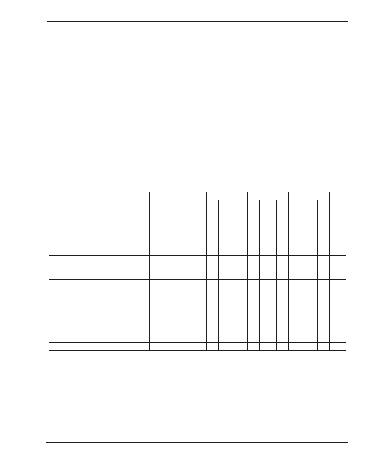
DC Electrical Characteristics (Note 7)
Symbol Parameter Conditions LF147 LF347B LF347 Units
Min Typ Max Min Typ Max Min Typ Max
V
OS
∆V
I
OS
I
B
R
IN
A
VOL
V
O
V
CM
CMRR Common-Mode Rejection Ratio R
PSRR Supply Voltage Rejection Ratio (Note 9) 80 100 80 100 70 100 dB
I
S
Input Offset Voltage RS=10 kΩ,TA=25˚C 1 5 3 5 5 10 mV
Over Temperature 8 7 13 mV
/∆T Average TC of Input Offset RS=10 kΩ 10 10 10 µV/˚C
OS
Voltage
Input Offset Current Tj=25˚C, (Notes 7, 8) 25 100 25 100 25 100 pA
Over Temperature 25 4 4 nA
Input Bias Current Tj=25˚C, (Notes 7, 8) 50 200 50 200 50 200 pA
Over Temperature 50 8 8 nA
Input Resistance Tj=25˚C 10
12
10
12
10
12
Large Signal Voltage Gain VS=±15V, TA=25˚C 50 100 50 100 25 100 V/mV
V
=±10V, RL=2 kΩ
O
Over Temperature 25 25 15 V/mV
Output Voltage Swing VS=±15V, RL=10 kΩ
Input Common-Mode Voltage VS=±15V
±12±
±
11 +15
13.5
±12±
±
11 +15
13.5
±12±
13.5 V
±
11 +15 V
Range −12 −12 −12 V
≤10 kΩ 80 100 80 100 70 100 dB
S
Supply Current 7.2 11 7.2 11 7.2 11 mA
Ω
www.national.com 2
Page 3
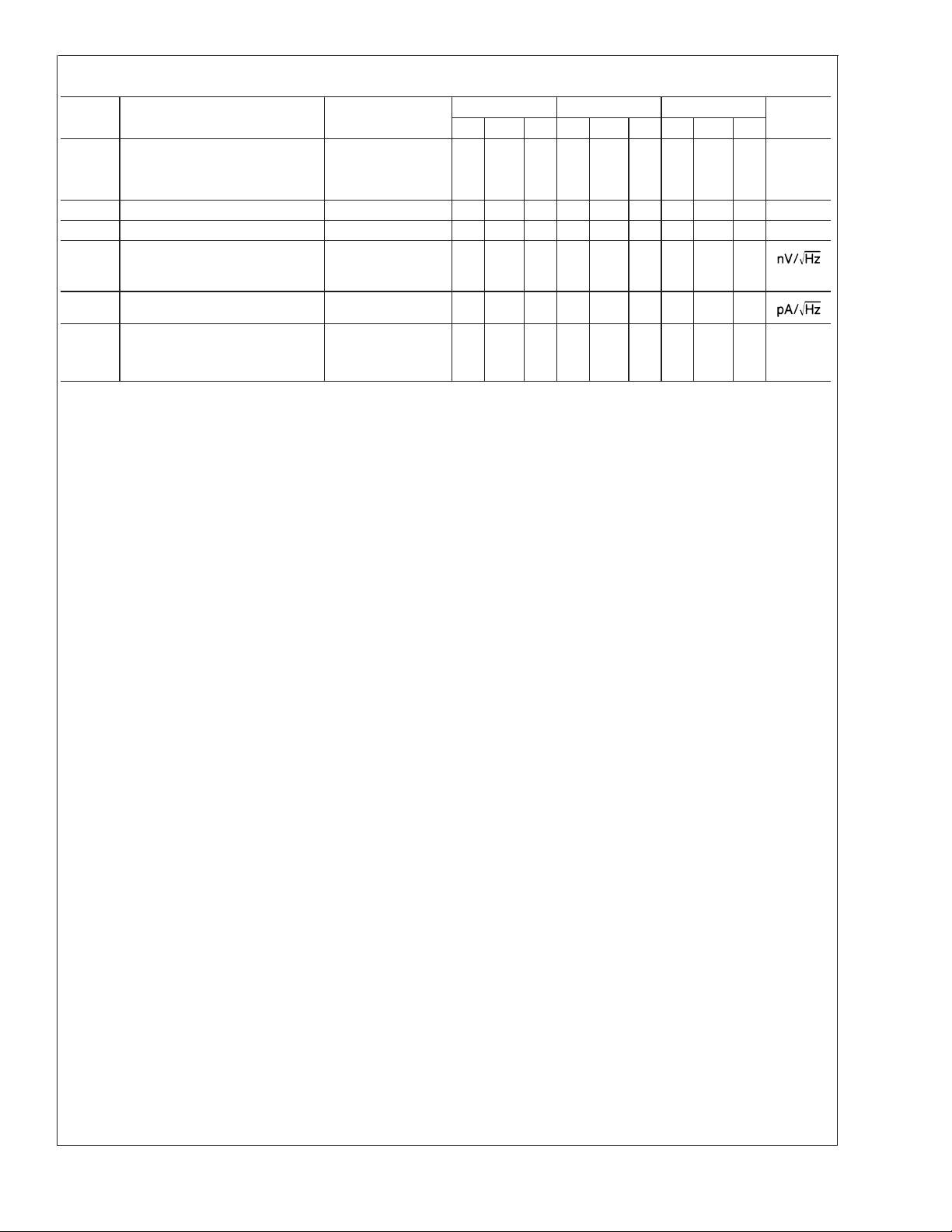
AC Electrical Characteristics (Note 7)
Symbol Parameter Conditions LF147 LF347B LF347 Units
Min Typ Max Min Typ Max Min Typ Max
Amplifier to Amplifier Coupling T
SR Slew Rate V
GBW Gain-Bandwidth Product V
e
n
i
n
Equivalent Input Noise Voltage TA=25˚C, RS=100Ω,202020
Equivalent Input Noise Current Tj=25˚C, f=1000 Hz 0.01 0.01 0.01
=25˚C, −120 −120 −120 dB
A
f=1 Hz−20 kHz
(Input Referred)
=±15V, TA=25˚C 8 13 8 13 8 13 V/µs
S
=±15V, TA=25˚C 2.2 4 2.2 4 2.2 4 MHz
S
f=1000 Hz
LF147/LF347
THD Total Harmonic Distortion AV=+10, RL=10k,
=20 Vp-p,
V
O
<
0.02
<
0.02
<
0.02 %
BW=20 Hz−20 kHz
Note 2: Absolute Maximum Ratings indicate limits beyond which damage to the device may occur. Operating Ratings indicate conditions for which the device is
functional, but do not guarantee specific performance limits.
Note 3: Unless otherwise specified the absolute maximum negative input voltage is equal to the negative power supply voltage.
Note 4: Any of the amplifier outputs can be shorted to ground indefinitely, however, more than one should not be simultaneously shorted as the maximum junction
temperature will be exceeded.
Note 5: For operating at elevated temperature, these devices must be derated based on a thermal resistance of θ
Note 6: The LF147 is available in the military temperature range −55˚C≤T
range 0˚C≤T
Note 7: Unless otherwise specified the specifications apply over the full temperature range and for V
V
OS,IB
Note 8: The input bias currents are junction leakage currents which approximately double for every 10˚C increase in the junction temperature, T
production test time, the input bias currents measured are correlated to junction temperature. In normal operation the junction temperature rises above the ambient
temperature as a result of internal power dissipation, P
recommended if input bias current is to be kept to a minimum.
Note 9: Supply voltage rejection ratio is measured for both supply magnitudes increasing or decreasing simultaneously in accordance with common practice from
V
=±5V to±15V for the LF347 and LF347B and from VS=±20V to±5V for the LF147.
S
Note 10: Refer to RETS147X for LF147D and LF147J military specifications.
Note 11: Max. Power Dissipation is defined by the package characteristics. Operating the part near the Max. Power Dissipation may cause the part to operate
outside guaranteed limits.
Note 12: Human body model, 1.5 kΩ in series with 100 pF.
≤70˚C. Junction temperature can rise to Tjmax = 150˚C.
A
, and IOSare measured at VCM=0.
D.Tj=TA+θjAPD
≤125˚C, while the LF347B and the LF347 are available in the commercial temperature
A
=±20V for the LF147 and for VS=±15V for the LF347B/LF347.
S
where θjAis the thermal resistance from junction to ambient. Use of a heat sink is
.
jA
. Due to limited
j
www.national.com3
Page 4
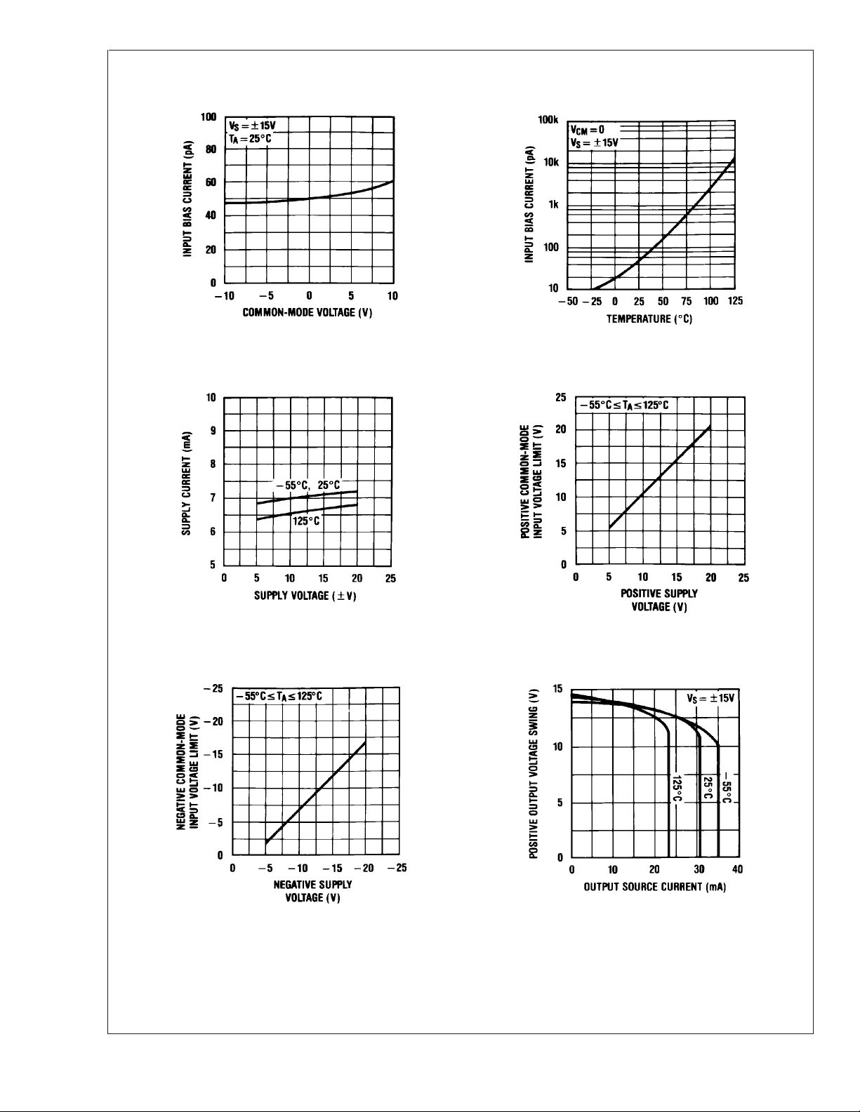
Typical Performance Characteristics
Input Bias Current Input Bias Current
LF147/LF347
00564714
Positive Common-Mode
Supply Current
00564716
Input Voltage Limit
Negative Common-Mode
Input Voltage Limit Positive Current Limit
00564715
00564717
00564718
www.national.com 4
00564719
Page 5
Typical Performance Characteristics (Continued)
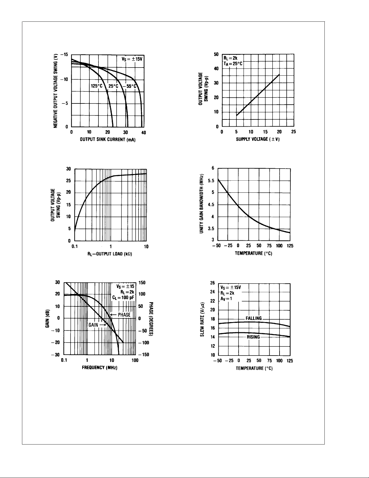
Negative Current Limit Output Voltage Swing
LF147/LF347
00564720
Output Voltage Swing Gain Bandwidth
00564722
Bode Plot Slew Rate
00564721
00564723
00564724
00564725
www.national.com5
Page 6
Typical Performance Characteristics (Continued)
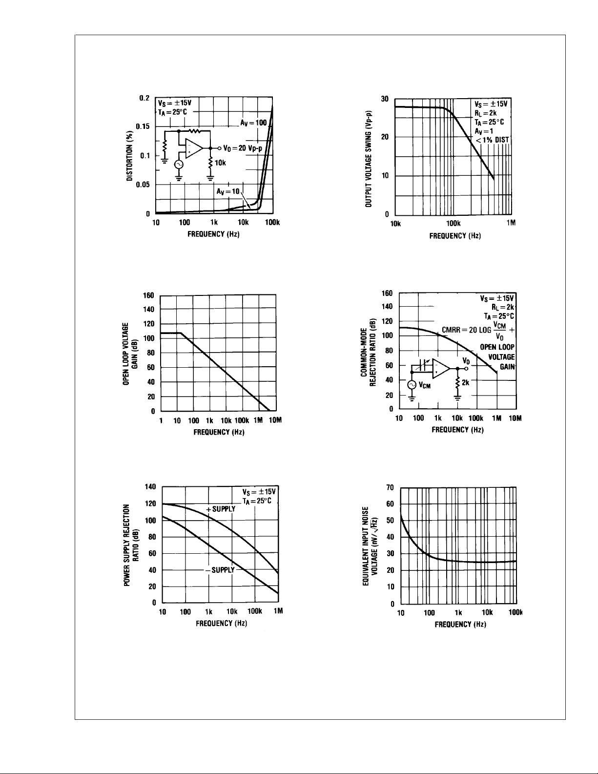
Distortion vs Frequency
LF147/LF347
Undistorted Output Voltage
Swing
Open Loop Frequency
Response
Power Supply Rejection
Ratio
00564726
00564728
00564727
Common-Mode Rejection
Ratio
00564729
Equivalent Input Noise
Voltage
00564730 00564731
www.national.com 6
Page 7
Typical Performance Characteristics (Continued)
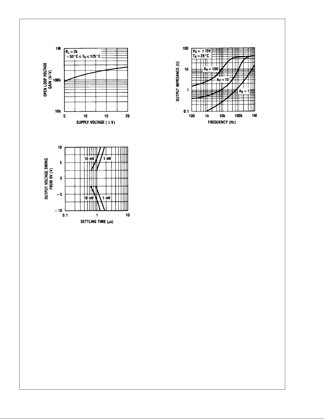
Open Loop Voltage Gain Output Impedance
LF147/LF347
Inverter Settling Time
00564732
00564734
00564733
www.national.com7
Page 8
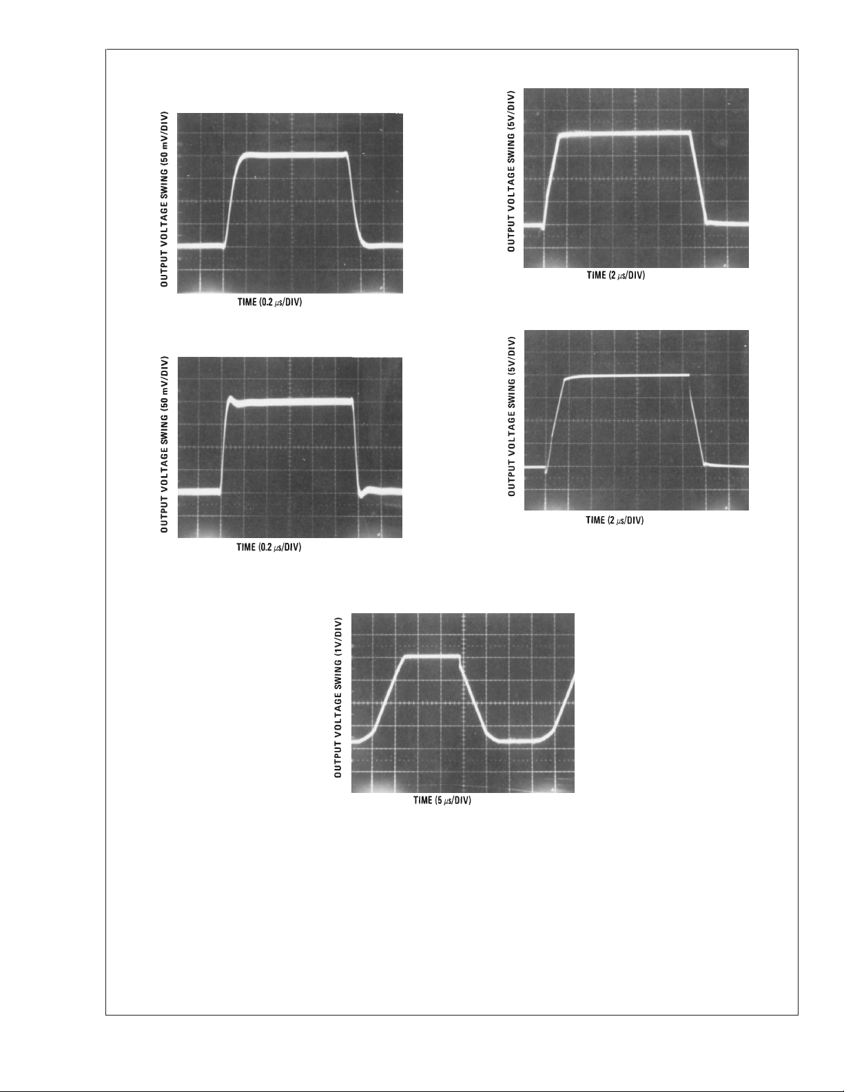
Pulse Response R
LF147/LF347
=2 kΩ,CL=10 pF
L
Small Signal Inverting
Large Signal Inverting
00564706
Small Signal Non-Inverting
00564704
00564705
Current Limit (RL=100Ω)
Large Signal Non-Inverting
00564707
Application Hints
The LF147 is an op amp with an internally trimmed input
offset voltage and JFET input devices (BI-FET II). These
JFETs have large reverse breakdown voltages from gate to
source and drain eliminating the need for clamps across the
inputs. Therefore, large differential input voltages can easily
be accommodated without a large increase in input current.
The maximum differential input voltage is independent of the
supply voltages. However, neither of the input voltages
www.national.com 8
00564708
should be allowed to exceed the negative supply as this will
cause large currents to flow which can result in a destroyed
unit.
Exceeding the negative common-mode limit on either input
will force the output to a high state, potentially causing a
reversal of phase to the output. Exceeding the negative
common-mode limit on both inputs will force the amplifier
output to a high state. In neither case does a latch occur
since raising the input back within the common-mode range
again puts the input stage and thus the amplifier in a normal
operating mode.
Page 9
Application Hints (Continued)
Exceeding the positive common-mode limit on a single input
will not change the phase of the output; however, if both
inputs exceed the limit, the output of the amplifier will be
forced to a high state.
The amplifiers will operate with a common-mode input voltage equal to the positive supply; however, the gain bandwidth and slew rate may be decreased in this condition.
When the negative common-mode voltage swings to within
3V of the negative supply, an increase in input offset voltage
may occur.
Each amplifier is individually biased by a zener reference
which allows normal circuit operation on
plies. Supply voltages less than these may result in lower
gain bandwidth and slew rate.
The LF147 will drivea2kΩ load resistance to
full temperature range. If the amplifier is forced to drive
heavier load currents, however, an increase in input offset
voltage may occur on the negative voltage swing and finally
reach an active current limit on both positive and negative
swings.
Precautions should be taken to ensure that the power supply
for the integrated circuit never becomes reversed in polarity
or that the unit is not inadvertently installed backwards in a
±
4.5V power sup-
±
10V over the
LF147/LF347
socket as an unlimited current surge through the resulting
forward diode within the IC could cause fusing of the internal
conductors and result in a destroyed unit.
As with most amplifiers, care should be taken with lead
dress, component placement and supply decoupling in order
to ensure stability. For example, resistors from the output to
an input should be placed with the body close to the input to
minimize “pick-up” and maximize the frequency of the feedback pole by minimizing the capacitance from the input to
ground.
A feedback pole is created when the feedback around any
amplifier is resistive. The parallel resistance and capacitance
from the input of the device (usually the inverting input) to AC
ground set the frequency of the pole. In many instances the
frequency of this pole is much greater than the expected 3
dB frequency of the closed loop gain and consequently there
is negligible effect on stability margin. However, if the feedback pole is less than approximately 6 times the expected 3
dB frequency a lead capacitor should be placed from the
output to the input of the op amp. The value of the added
capacitor should be such that the RC time constant of this
capacitor and the resistance it parallels is greater than or
equal to the original feedback pole time constant.
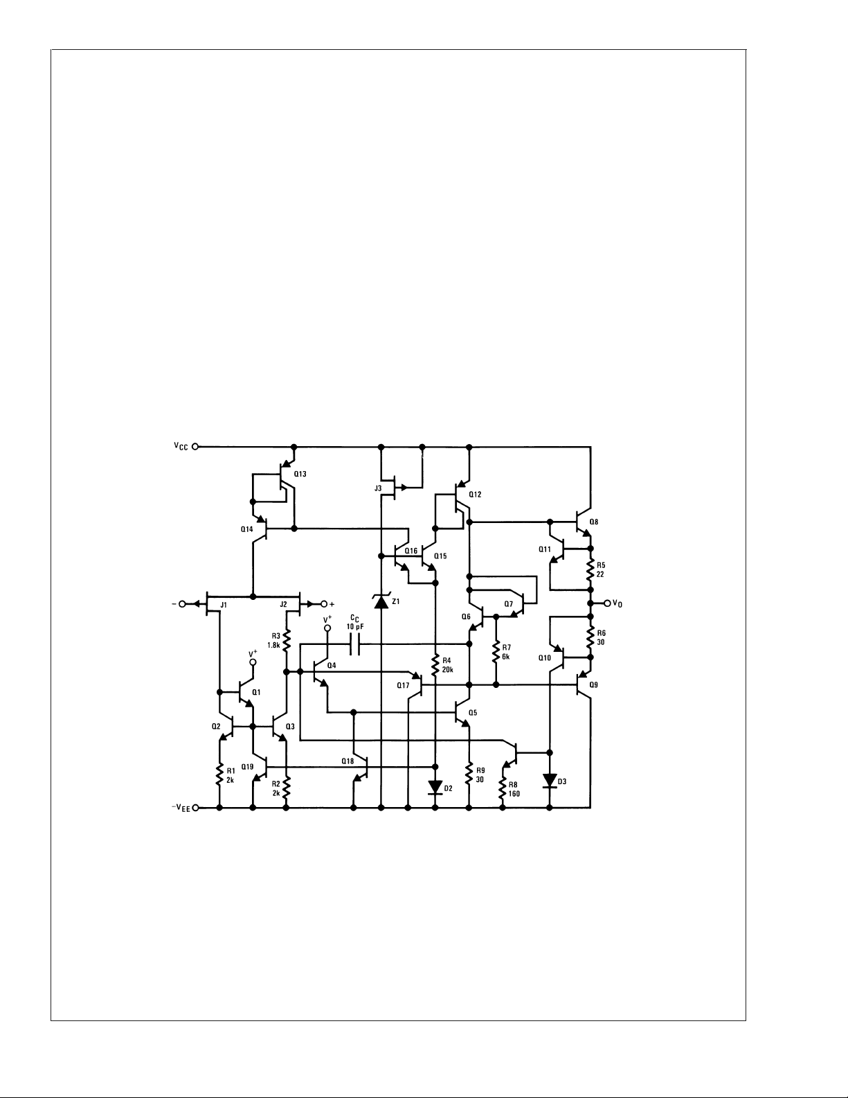
Detailed Schematic
00564709
www.national.com9
Page 10
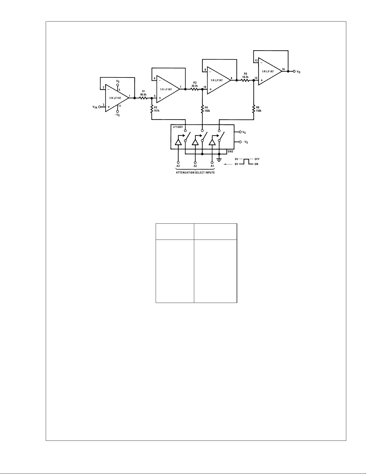
Typical Applications
LF147/LF347
Digitally Selectable Precision Attenuator
All resistors 1% tolerance
Accuracy of better than 0.4% with standard 1% value resistors
•
No offset adjustment necessary
Expandable to any number of stages
•
Very high input impedance
•
A1 A2 A3 V
000 0
001 −1dB
010 −2dB
011 −3dB
100 −4dB
101 −5dB
110 −6dB
111 −7dB
00564710
O
Attenuation
www.national.com 10
Page 11
Typical Applications (Continued)
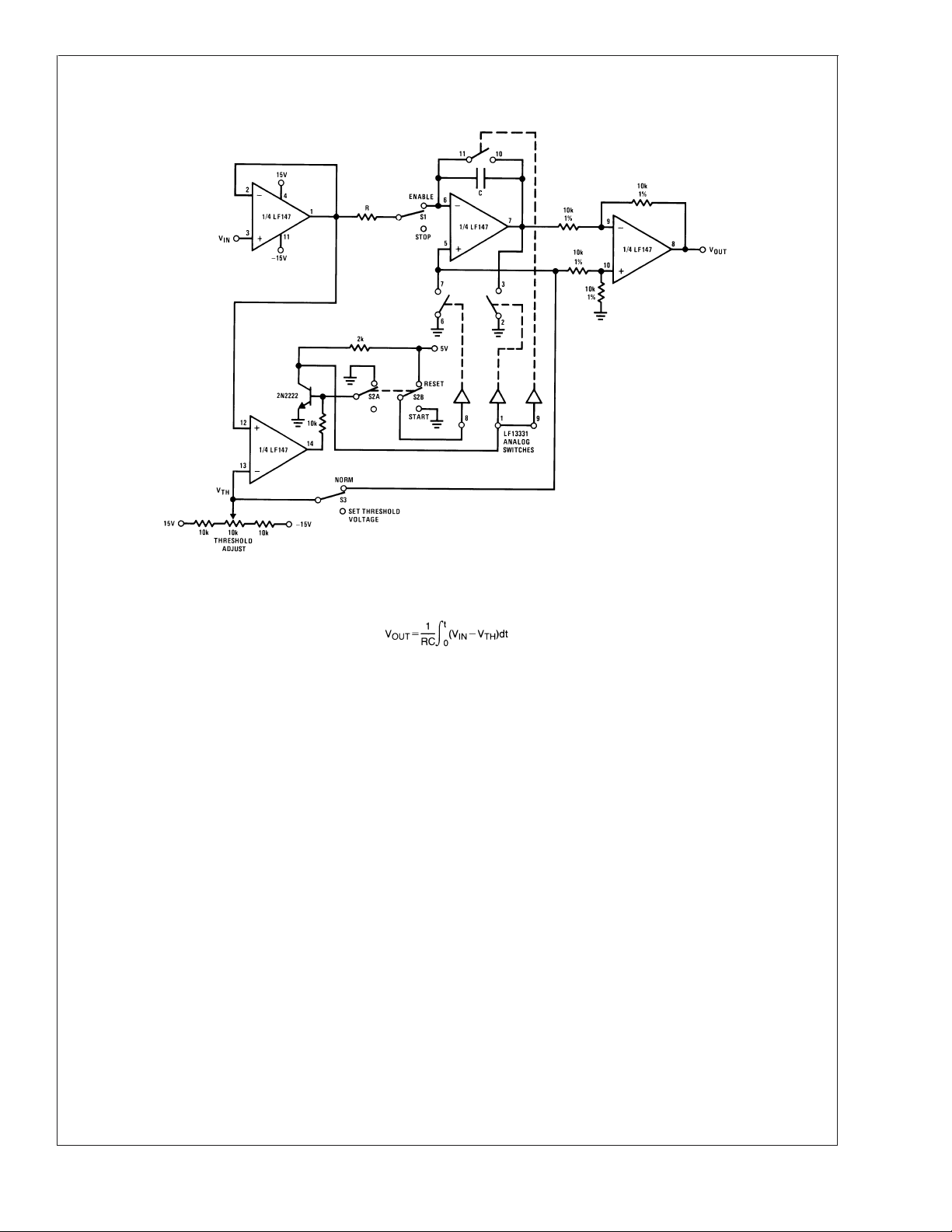
Long Time Integrator with Reset, Hold and Starting Threshold Adjustment
LF147/LF347
V
•
•
•
•
starts from zero and is equal to the integral of the input voltage with respect to the threshold voltage:
OUT
Output starts when VIN≥V
TH
Switch S1 permits stopping and holding any output value
Switch S2 resets system to zero
00564711
www.national.com11
Page 12
Typical Applications (Continued)
LF147/LF347
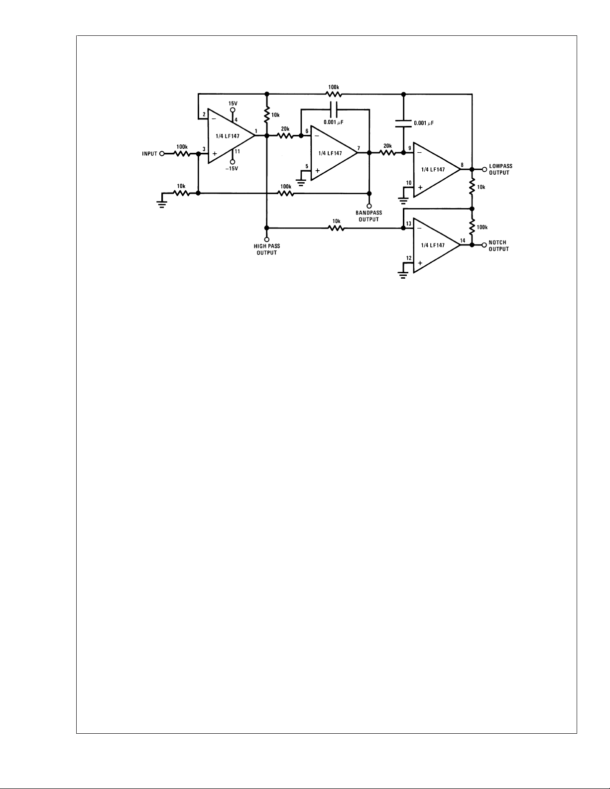
Universal State Variable Filter
For circuit shown:
=3 kHz, f
f
o
Q=3.4
Passband gain:
Highpass —0.1
Bandpass —1
Lowpass —1
Notch —10
foxQ≤200 kHz
•
10V peak sinusoidal output swing without slew limiting to 200 kHz
•
See LM148 data sheet for design equations
•
NOTCH
=9.5 kHz
00564712
www.national.com 12
Page 13
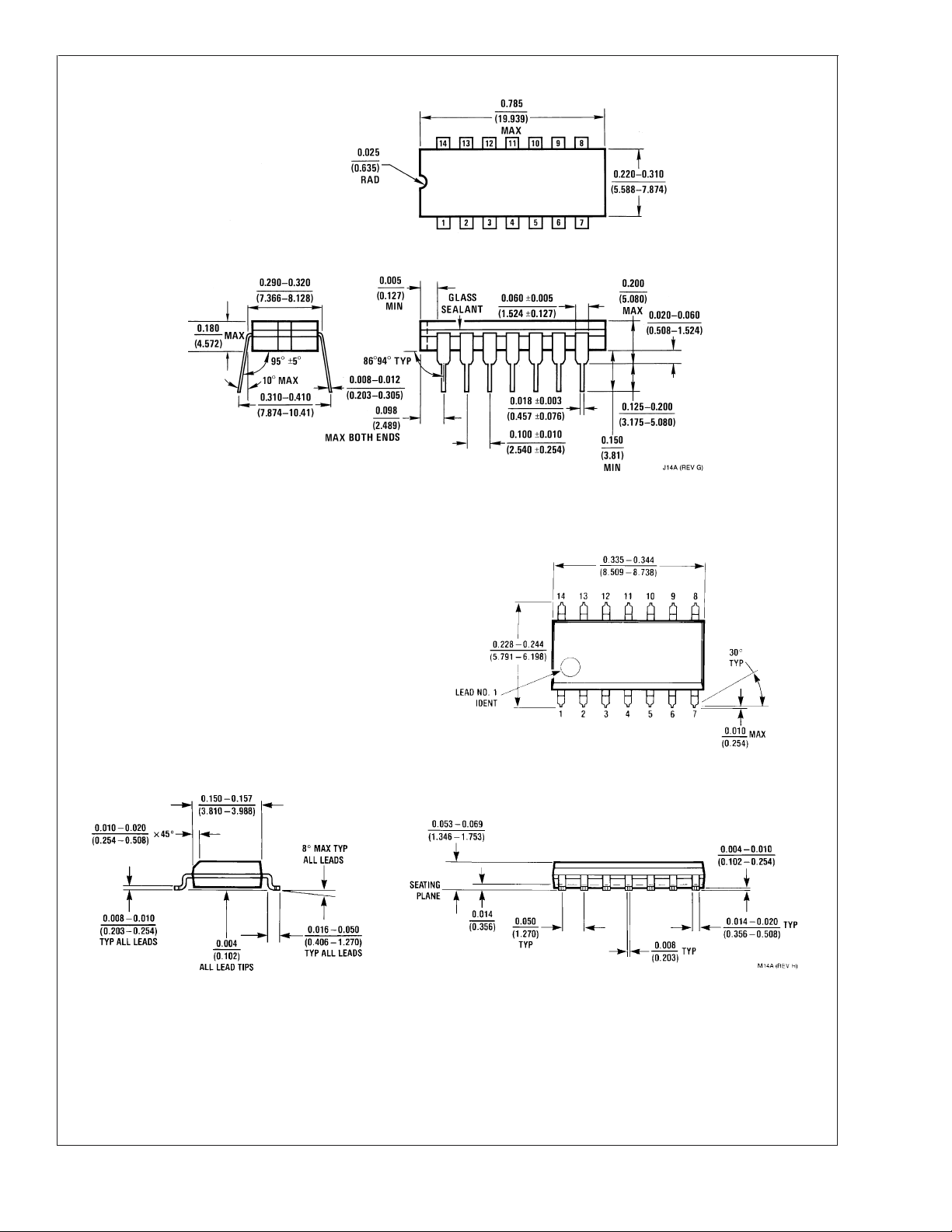
Physical Dimensions inches (millimeters) unless otherwise noted
Ceramic Dual-In-Line Package (J)
Order Number LF147J, LM147J-SMD or LF147J/883
NS Package Number J14A
LF147/LF347
S.O. Package (M)
Order Number LF347M or LF347MX
NS Package Number M14A
www.national.com13
Page 14
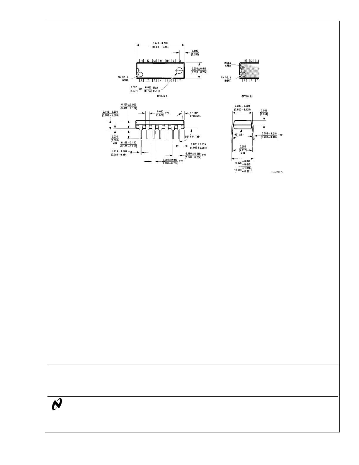
Physical Dimensions inches (millimeters) unless otherwise noted (Continued)
Molded Dual-In-Line Package (N)
Order Number LF347BN or LF347N
NS Package Number N14A
LIFE SUPPORT POLICY
NATIONAL’S PRODUCTS ARE NOT AUTHORIZED FOR USE AS CRITICAL COMPONENTS IN LIFE SUPPORT
DEVICES OR SYSTEMS WITHOUT THE EXPRESS WRITTEN APPROVAL OF THE PRESIDENT AND GENERAL
COUNSEL OF NATIONAL SEMICONDUCTOR CORPORATION. As used herein:
LF147/LF347 Wide Bandwidth Quad JFET Input Operational Amplifiers
1. Life support devices or systems are devices or
systems which, (a) are intended for surgical implant
into the body, or (b) support or sustain life, and
whose failure to perform when properly used in
accordance with instructions for use provided in the
2. A critical component is any component of a life
support device or system whose failure to perform
can be reasonably expected to cause the failure of
the life support device or system, or to affect its
safety or effectiveness.
labeling, can be reasonably expected to result in a
significant injury to the user.
BANNED SUBSTANCE COMPLIANCE
National Semiconductor certifies that the products and packing materials meet the provisions of the Customer Products
Stewardship Specification (CSP-9-111C2) and the Banned Substances and Materials of Interest Specification
(CSP-9-111S2) and contain no ‘‘Banned Substances’’ as defined in CSP-9-111S2.
National Semiconductor
Americas Customer
Support Center
Email: [email protected]
Tel: 1-800-272-9959
www.national.com
National does not assume any responsibility for use of any circuitry described, no circuit patent licenses are implied and National reserves the right at any time without notice to change said circuitry and specifications.
National Semiconductor
Europe Customer Support Center
Fax: +49 (0) 180-530 85 86
Email: [email protected]
Deutsch Tel: +49 (0) 69 9508 6208
English Tel: +44 (0) 870 24 0 2171
Français Tel: +33 (0) 1 41 91 8790
National Semiconductor
Asia Pacific Customer
Support Center
Email: [email protected]
National Semiconductor
Japan Customer Support Center
Fax: 81-3-5639-7507
Email: [email protected]
Tel: 81-3-5639-7560
 Loading...