

Page 1

8-bit AVR Microcontrollers
ATmega328/P
DATASHEET COMPLETE
Introduction
The Atmel
®
picoPower
®
ATmega328/P is a low-power CMOS 8-bit
microcontroller based on the AVR
®
enhanced RISC architecture. By
executing powerful instructions in a single clock cycle, the ATmega328/P
achieves throughputs close to 1MIPS per MHz. This empowers system
designer to optimize the device for power consumption versus processing
speed.
Feature
High Performance, Low Power Atmel
®
AVR
®
8-Bit Microcontroller Family
• Advanced RISC Architecture
– 131 Powerful Instructions
– Most Single Clock Cycle Execution
– 32 x 8 General Purpose Working Registers
– Fully Static Operation
– Up to 20 MIPS Throughput at 20MHz
– On-chip 2-cycle Multiplier
• High Endurance Non-volatile Memory Segments
– 32KBytes of In-System Self-Programmable Flash program
Memory
– 1KBytes EEPROM
– 2KBytes Internal SRAM
– Write/Erase Cycles: 10,000 Flash/100,000 EEPROM
– Data Retention: 20 years at 85°C/100 years at 25°C
(1)
– Optional Boot Code Section with Independent Lock Bits
• In-System Programming by On-chip Boot Program
• True Read-While-Write Operation
– Programming Lock for Software Security
• Atmel
®
QTouch
®
Library Support
– Capacitive Touch Buttons, Sliders and Wheels
– QTouch and QMatrix
®
Acquisition
– Up to 64 sense channels
Atmel-42735B-ATmega328/P_Datasheet_Complete-11/2016
Page 2

• Peripheral Features
– Two 8-bit Timer/Counters with Separate Prescaler and Compare Mode
– One 16-bit Timer/Counter with Separate Prescaler, Compare Mode, and Capture Mode
– Real Time Counter with Separate Oscillator
– Six PWM Channels
– 8-channel 10-bit ADC in TQFP and QFN/MLF package
• Temperature Measurement
– 6-channel 10-bit ADC in PDIP Package
• Temperature Measurement
– Two Master/Slave SPI Serial Interface
– One Programmable Serial USART
– One Byte-oriented 2-wire Serial Interface (Philips I
2
C compatible)
– Programmable Watchdog Timer with Separate On-chip Oscillator
– One On-chip Analog Comparator
– Interrupt and Wake-up on Pin Change
• Special Microcontroller Features
– Power-on Reset and Programmable Brown-out Detection
– Internal Calibrated Oscillator
– External and Internal Interrupt Sources
– Six Sleep Modes: Idle, ADC Noise Reduction, Power-save, Power-down, Standby, and
Extended Standby
• I/O and Packages
– 23 Programmable I/O Lines
– 28-pin PDIP, 32-lead TQFP, 28-pad QFN/MLF and 32-pad QFN/MLF
• Operating Voltage:
– 1.8 - 5.5V
• Temperature Range:
– -40°C to 105°C
• Speed Grade:
– 0 - 4MHz @ 1.8 - 5.5V
– 0 - 10MHz @ 2.7 - 5.5V
– 0 - 20MHz @ 4.5 - 5.5V
• Power Consumption at 1MHz, 1.8V, 25°C
– Active Mode: 0.2mA
– Power-down Mode: 0.1μA
– Power-save Mode: 0.75μA (Including 32kHz RTC)
Atmel ATmega328/P [DATASHEET]
Atmel-42735B-ATmega328/P_Datasheet_Complete-11/2016
2
Page 3

Table of Contents
Introduction......................................................................................................................1
Feature............................................................................................................................ 1
1. Description.................................................................................................................9
2. Configuration Summary...........................................................................................10
3. Ordering Information ............................................................................................... 11
3.1. ATmega328 ............................................................................................................................... 11
3.2. ATmega328P .............................................................................................................................12
4. Block Diagram......................................................................................................... 13
5. Pin Configurations................................................................................................... 14
5.1. Pin-out........................................................................................................................................14
5.2. Pin Descriptions..........................................................................................................................17
6. I/O Multiplexing........................................................................................................19
7. Resources................................................................................................................21
8. Data Retention.........................................................................................................22
9. About Code Examples.............................................................................................23
10. Capacitive Touch Sensing....................................................................................... 24
10.1. QTouch Library........................................................................................................................... 24
11. AVR CPU Core........................................................................................................ 25
11.1. Overview.....................................................................................................................................25
11.2. ALU – Arithmetic Logic Unit........................................................................................................26
11.3. Status Register...........................................................................................................................26
11.4. General Purpose Register File................................................................................................... 28
11.5. Stack Pointer.............................................................................................................................. 29
11.6. Instruction Execution Timing...................................................................................................... 31
11.7. Reset and Interrupt Handling..................................................................................................... 32
12. AVR Memories.........................................................................................................34
12.1. Overview.....................................................................................................................................34
12.2. In-System Reprogrammable Flash Program Memory................................................................34
12.3. SRAM Data Memory...................................................................................................................35
12.4. EEPROM Data Memory............................................................................................................. 36
12.5. I/O Memory.................................................................................................................................37
12.6. Register Description................................................................................................................... 38
13. System Clock and Clock Options............................................................................ 48
Page 4

13.1. Clock Systems and Their Distribution.........................................................................................48
13.2. Clock Sources............................................................................................................................ 49
13.3. Low Power Crystal Oscillator......................................................................................................51
13.4. Full Swing Crystal Oscillator.......................................................................................................52
13.5. Low Frequency Crystal Oscillator...............................................................................................53
13.6. Calibrated Internal RC Oscillator................................................................................................54
13.7. 128kHz Internal Oscillator.......................................................................................................... 55
13.8. External Clock............................................................................................................................ 56
13.9. Timer/Counter Oscillator.............................................................................................................57
13.10. Clock Output Buffer....................................................................................................................57
13.11. System Clock Prescaler............................................................................................................. 57
13.12. Register Description...................................................................................................................58
14. PM - Power Management and Sleep Modes...........................................................62
14.1. Overview.....................................................................................................................................62
14.2. Sleep Modes...............................................................................................................................62
14.3. BOD Disable...............................................................................................................................63
14.4. Idle Mode....................................................................................................................................63
14.5. ADC Noise Reduction Mode.......................................................................................................63
14.6. Power-Down Mode.....................................................................................................................64
14.7. Power-save Mode.......................................................................................................................64
14.8. Standby Mode............................................................................................................................ 65
14.9. Extended Standby Mode............................................................................................................ 65
14.10. Power Reduction Register......................................................................................................... 65
14.11. Minimizing Power Consumption................................................................................................. 65
14.12. Register Description...................................................................................................................67
15. SCRST - System Control and Reset....................................................................... 72
15.1. Resetting the AVR......................................................................................................................72
15.2. Reset Sources............................................................................................................................72
15.3. Power-on Reset..........................................................................................................................73
15.4. External Reset............................................................................................................................74
15.5. Brown-out Detection...................................................................................................................74
15.6. Watchdog System Reset............................................................................................................75
15.7. Internal Voltage Reference.........................................................................................................75
15.8. Watchdog Timer......................................................................................................................... 76
15.9. Register Description................................................................................................................... 78
16. Interrupts................................................................................................................. 82
16.1. Interrupt Vectors in ATmega328/P..............................................................................................82
16.2. Register Description................................................................................................................... 84
17. EXINT - External Interrupts..................................................................................... 87
17.1. Pin Change Interrupt Timing.......................................................................................................87
17.2. Register Description................................................................................................................... 88
18. I/O-Ports.................................................................................................................. 97
18.1. Overview.....................................................................................................................................97
18.2. Ports as General Digital I/O........................................................................................................98
Atmel ATmega328/P [DATASHEET]
Atmel-42735B-ATmega328/P_Datasheet_Complete-11/2016
4
Page 5

18.3. Alternate Port Functions...........................................................................................................101
18.4. Register Description................................................................................................................. 113
19. TC0 - 8-bit Timer/Counter0 with PWM...................................................................125
19.1. Features................................................................................................................................... 125
19.2. Overview...................................................................................................................................125
19.3. Timer/Counter Clock Sources.................................................................................................. 127
19.4. Counter Unit............................................................................................................................. 127
19.5. Output Compare Unit................................................................................................................128
19.6. Compare Match Output Unit.....................................................................................................130
19.7. Modes of Operation..................................................................................................................131
19.8. Timer/Counter Timing Diagrams...............................................................................................135
19.9. Register Description................................................................................................................. 137
20. TC1 - 16-bit Timer/Counter1 with PWM.................................................................149
20.1. Overview...................................................................................................................................149
20.2. Features................................................................................................................................... 149
20.3. Block Diagram.......................................................................................................................... 149
20.4. Definitions.................................................................................................................................150
20.5. Registers.................................................................................................................................. 151
20.6. Accessing 16-bit Registers.......................................................................................................151
20.7. Timer/Counter Clock Sources.................................................................................................. 154
20.8. Counter Unit............................................................................................................................. 154
20.9. Input Capture Unit.................................................................................................................... 155
20.10. Output Compare Units............................................................................................................. 157
20.11. Compare Match Output Unit.....................................................................................................159
20.12. Modes of Operation..................................................................................................................160
20.13. Timer/Counter Timing Diagrams.............................................................................................. 168
20.14. Register Description.................................................................................................................169
21. Timer/Counter 0, 1 Prescalers...............................................................................186
21.1. Internal Clock Source............................................................................................................... 186
21.2. Prescaler Reset........................................................................................................................186
21.3. External Clock Source..............................................................................................................186
21.4. Register Description................................................................................................................. 187
22. TC2 - 8-bit Timer/Counter2 with PWM and Asynchronous Operation...................189
22.1. Features................................................................................................................................... 189
22.2. Overview...................................................................................................................................189
22.3. Timer/Counter Clock Sources.................................................................................................. 191
22.4. Counter Unit............................................................................................................................. 191
22.5. Output Compare Unit................................................................................................................192
22.6. Compare Match Output Unit.....................................................................................................194
22.7. Modes of Operation..................................................................................................................195
22.8. Timer/Counter Timing Diagrams...............................................................................................199
22.9. Asynchronous Operation of Timer/Counter2............................................................................200
22.10. Timer/Counter Prescaler.......................................................................................................... 202
22.11. Register Description.................................................................................................................202
Atmel ATmega328/P [DATASHEET]
Atmel-42735B-ATmega328/P_Datasheet_Complete-11/2016
5
Page 6

23. SPI – Serial Peripheral Interface........................................................................... 215
23.1. Features................................................................................................................................... 215
23.2. Overview...................................................................................................................................215
23.3. SS Pin Functionality................................................................................................................. 219
23.4. Data Modes.............................................................................................................................. 219
23.5. Register Description................................................................................................................. 220
24. USART - Universal Synchronous Asynchronous Receiver Transceiver................225
24.1. Features................................................................................................................................... 225
24.2. Overview...................................................................................................................................225
24.3. Block Diagram.......................................................................................................................... 225
24.4. Clock Generation......................................................................................................................226
24.5. Frame Formats.........................................................................................................................229
24.6. USART Initialization..................................................................................................................230
24.7. Data Transmission – The USART Transmitter......................................................................... 231
24.8. Data Reception – The USART Receiver.................................................................................. 233
24.9. Asynchronous Data Reception.................................................................................................237
24.10. Multi-Processor Communication Mode.................................................................................... 239
24.11. Examples of Baud Rate Setting............................................................................................... 240
24.12. Register Description.................................................................................................................243
25. USARTSPI - USART in SPI Mode.........................................................................254
25.1. Features................................................................................................................................... 254
25.2. Overview...................................................................................................................................254
25.3. Clock Generation......................................................................................................................254
25.4. SPI Data Modes and Timing.....................................................................................................255
25.5. Frame Formats.........................................................................................................................255
25.6. Data Transfer............................................................................................................................257
25.7. AVR USART MSPIM vs. AVR SPI............................................................................................258
25.8. Register Description................................................................................................................. 259
26. TWI - 2-wire Serial Interface..................................................................................260
26.1. Features................................................................................................................................... 260
26.2. Two-Wire Serial Interface Bus Definition..................................................................................260
26.3. Data Transfer and Frame Format.............................................................................................261
26.4. Multi-master Bus Systems, Arbitration and Synchronization....................................................264
26.5. Overview of the TWI Module.................................................................................................... 266
26.6. Using the TWI...........................................................................................................................268
26.7. Transmission Modes................................................................................................................ 271
26.8. Multi-master Systems and Arbitration.......................................................................................289
26.9. Register Description................................................................................................................. 291
27. AC - Analog Comparator....................................................................................... 299
27.1. Overview...................................................................................................................................299
27.2. Analog Comparator Multiplexed Input...................................................................................... 299
27.3. Register Description................................................................................................................. 300
28. ADC - Analog to Digital Converter.........................................................................305
Atmel ATmega328/P [DATASHEET]
Atmel-42735B-ATmega328/P_Datasheet_Complete-11/2016
6
Page 7

28.1. Features................................................................................................................................... 305
28.2. Overview...................................................................................................................................305
28.3. Starting a Conversion...............................................................................................................307
28.4. Prescaling and Conversion Timing...........................................................................................308
28.5. Changing Channel or Reference Selection.............................................................................. 310
28.6. ADC Noise Canceler................................................................................................................ 312
28.7. ADC Conversion Result............................................................................................................315
28.8. Temperature Measurement...................................................................................................... 316
28.9. Register Description................................................................................................................. 316
29. DBG - debugWIRE On-chip Debug System.......................................................... 327
29.1. Features................................................................................................................................... 327
29.2. Overview...................................................................................................................................327
29.3. Physical Interface..................................................................................................................... 327
29.4. Software Break Points..............................................................................................................328
29.5. Limitations of debugWIRE........................................................................................................328
29.6. Register Description................................................................................................................. 328
30. BTLDR - Boot Loader Support – Read-While-Write Self-Programming................ 330
30.1. Features................................................................................................................................... 330
30.2. Overview...................................................................................................................................330
30.3. Application and Boot Loader Flash Sections............................................................................330
30.4. Read-While-Write and No Read-While-Write Flash Sections...................................................331
30.5. Boot Loader Lock Bits.............................................................................................................. 333
30.6. Entering the Boot Loader Program...........................................................................................334
30.7. Addressing the Flash During Self-Programming...................................................................... 335
30.8. Self-Programming the Flash.....................................................................................................336
30.9. Register Description................................................................................................................. 344
31. MEMPROG- Memory Programming......................................................................347
31.1. Program And Data Memory Lock Bits...................................................................................... 347
31.2. Fuse Bits...................................................................................................................................348
31.3. Signature Bytes........................................................................................................................ 350
31.4. Calibration Byte........................................................................................................................ 351
31.5. Page Size................................................................................................................................. 351
31.6. Parallel Programming Parameters, Pin Mapping, and Commands..........................................351
31.7. Parallel Programming...............................................................................................................353
31.8. Serial Downloading...................................................................................................................360
32. Electrical Characteristics....................................................................................... 365
32.1. Absolute Maximum Ratings......................................................................................................365
32.2. Common DC Characteristics....................................................................................................365
32.3. Speed Grades.......................................................................................................................... 368
32.4. Clock Characteristics................................................................................................................369
32.5. System and Reset Characteristics........................................................................................... 370
32.6. SPI Timing Characteristics....................................................................................................... 371
32.7. Two-wire Serial Interface Characteristics.................................................................................372
32.8. ADC Characteristics................................................................................................................. 374
32.9. Parallel Programming Characteristics...................................................................................... 375
Atmel ATmega328/P [DATASHEET]
Atmel-42735B-ATmega328/P_Datasheet_Complete-11/2016
7
Page 8

33. Typical Characteristics (T
A
= -40°C to 85°C).........................................................378
33.1. ATmega328 Typical Characteristics......................................................................................... 378
34. Typical Characteristics (T
A
= -40°C to 105°C).......................................................403
34.1. ATmega328P Typical Characteristics....................................................................................... 403
35. Register Summary.................................................................................................428
35.1. Note..........................................................................................................................................430
36. Instruction Set Summary....................................................................................... 432
37. Packaging Information...........................................................................................436
37.1. 32-pin 32A................................................................................................................................ 436
37.2. 32-pin 32M1-A..........................................................................................................................437
37.3. 28-pin 28M1..............................................................................................................................438
37.4. 28-pin 28P3.............................................................................................................................. 439
38. Errata.....................................................................................................................440
38.1. Errata ATmega328/P................................................................................................................440
39. Datasheet Revision History................................................................................... 441
39.1. Rev. B – 11/2016...................................................................................................................... 441
39.2. Rev. A – 06/2016......................................................................................................................441
Atmel ATmega328/P [DATASHEET]
Atmel-42735B-ATmega328/P_Datasheet_Complete-11/2016
8
Page 9

1. Description
The Atmel AVR
®
core combines a rich instruction set with 32 general purpose working registers. All the
32 registers are directly connected to the Arithmetic Logic Unit (ALU), allowing two independent registers
to be accessed in a single instruction executed in one clock cycle. The resulting architecture is more code
efficient while achieving throughputs up to ten times faster than conventional CISC microcontrollers.
The ATmega328/P provides the following features: 32Kbytes of In-System Programmable Flash with
Read-While-Write capabilities, 1Kbytes EEPROM, 2Kbytes SRAM, 23 general purpose I/O lines, 32
general purpose working registers, Real Time Counter (RTC), three flexible Timer/Counters with compare
modes and PWM, 1 serial programmable USARTs , 1 byte-oriented 2-wire Serial Interface (I2C), a 6-
channel 10-bit ADC (8 channels in TQFP and QFN/MLF packages) , a programmable Watchdog Timer
with internal Oscillator, an SPI serial port, and six software selectable power saving modes. The Idle
mode stops the CPU while allowing the SRAM, Timer/Counters, SPI port, and interrupt system to
continue functioning. The Power-down mode saves the register contents but freezes the Oscillator,
disabling all other chip functions until the next interrupt or hardware reset. In Power-save mode, the
asynchronous timer continues to run, allowing the user to maintain a timer base while the rest of the
device is sleeping. The ADC Noise Reduction mode stops the CPU and all I/O modules except
asynchronous timer and ADC to minimize switching noise during ADC conversions. In Standby mode, the
crystal/resonator oscillator is running while the rest of the device is sleeping. This allows very fast start-up
combined with low power consumption. In Extended Standby mode, both the main oscillator and the
asynchronous timer continue to run.
Atmel offers the QTouch
®
library for embedding capacitive touch buttons, sliders and wheels functionality
into AVR microcontrollers. The patented charge-transfer signal acquisition offers robust sensing and
includes fully debounced reporting of touch keys and includes Adjacent Key Suppression
®
(AKS
™
)
technology for unambiguous detection of key events. The easy-to-use QTouch Suite toolchain allows you
to explore, develop and debug your own touch applications.
The device is manufactured using Atmel’s high density non-volatile memory technology. The On-chip ISP
Flash allows the program memory to be reprogrammed In-System through an SPI serial interface, by a
conventional nonvolatile memory programmer, or by an On-chip Boot program running on the AVR core.
The Boot program can use any interface to download the application program in the Application Flash
memory. Software in the Boot Flash section will continue to run while the Application Flash section is
updated, providing true Read-While-Write operation. By combining an 8-bit RISC CPU with In-System
Self-Programmable Flash on a monolithic chip, the Atmel ATmega328/P is a powerful microcontroller that
provides a highly flexible and cost effective solution to many embedded control applications.
The ATmega328/P is supported with a full suite of program and system development tools including: C
Compilers, Macro Assemblers, Program Debugger/Simulators, In-Circuit Emulators, and Evaluation kits.
Atmel ATmega328/P [DATASHEET]
Atmel-42735B-ATmega328/P_Datasheet_Complete-11/2016
9
Page 10

2. Configuration Summary
Features ATmega328/P
Pin Count 28/32
Flash (Bytes) 32K
SRAM (Bytes) 2K
EEPROM (Bytes) 1K
General Purpose I/O Lines 23
SPI 2
TWI (I
2
C) 1
USART 1
ADC 10-bit 15kSPS
ADC Channels 8
8-bit Timer/Counters 2
16-bit Timer/Counters 1
Atmel ATmega328/P [DATASHEET]
Atmel-42735B-ATmega328/P_Datasheet_Complete-11/2016
10
Page 11

3. Ordering Information
3.1. ATmega328
Speed [MHz]
(3)
Power Supply [V] Ordering Code
(2)
Package
(1)
Operational Range
20 1.8 - 5.5
ATmega328-AU
ATmega328-AUR
(5)
ATmega328-MMH
(4)
ATmega328-MMHR
(4)(5)
ATmega328-MU
ATmega328-MUR
(5)
ATmega328-PU
32A
32A
28M1
28M1
32M1-A
32M1-A
28P3
Industrial
(-40°C to 85°C)
Note:
1. This device can also be supplied in wafer form. Please contact your local Atmel sales office for
detailed ordering information and minimum quantities.
2. Pb-free packaging, complies to the European Directive for Restriction of Hazardous Substances
(RoHS directive). Also Halide free and fully Green.
3. Please refer to Speed Grades for Speed vs. V
CC
4. Tape & Reel.
5. NiPdAu Lead Finish.
Package Type
28M1 28-pad, 4 x 4 x 1.0 body, Lead Pitch 0.45mm Quad Flat No-Lead/Micro Lead Frame Package (QFN/
MLF)
28P3 28-lead, 0.300” Wide, Plastic Dual Inline Package (PDIP)
32M1-A 32-pad, 5 x 5 x 1.0 body, Lead Pitch 0.50mm Quad Flat No-Lead/Micro Lead Frame Package (QFN/
MLF)
32A 32-lead, Thin (1.0mm) Plastic Quad Flat Package (TQFP)
Atmel ATmega328/P [DATASHEET]
Atmel-42735B-ATmega328/P_Datasheet_Complete-11/2016
11
Page 12

3.2. ATmega328P
Speed [MHz]
(3)
Power Supply [V] Ordering Code
(2)
Package
(1)
Operational Range
20 1.8 - 5.5
ATmega328P-AU
ATmega328P-AUR
(5)
ATmega328P-MMH
(4)
ATmega328P-MMHR
(4)(5)
ATmega328P-MU
ATmega328P-MUR
(5)
ATmega328P-PU
32A
32A
28M1
28M1
32M1-A
32M1-A
28P3
Industrial
(-40°C to 85°C)
ATmega328P-AN
ATmega328P-ANR
(5)
ATmega328P-MN
ATmega328P-MNR
(5)
ATmega328P-PN
32A
32A
32M1-A
32M1-A
28P3
Industrial
(-40°C to 105°C)
Note:
1. This device can also be supplied in wafer form. Please contact your local Atmel sales office for
detailed ordering information and minimum quantities.
2. Pb-free packaging, complies to the European Directive for Restriction of Hazardous Substances
(RoHS directive). Also Halide free and fully Green.
3. Please refer to Speed Grades for Speed vs. V
CC
4. Tape & Reel.
5. NiPdAu Lead Finish.
Package Type
28M1 28-pad, 4 x 4 x 1.0 body, Lead Pitch 0.45mm Quad Flat No-Lead/Micro Lead Frame Package (QFN/
MLF)
28P3 28-lead, 0.300” Wide, Plastic Dual Inline Package (PDIP)
32M1-A 32-pad, 5 x 5 x 1.0 body, Lead Pitch 0.50mm Quad Flat No-Lead/Micro Lead Frame Package (QFN/
MLF)
32A 32-lead, Thin (1.0mm) Plastic Quad Flat Package (TQFP)
Atmel ATmega328/P [DATASHEET]
Atmel-42735B-ATmega328/P_Datasheet_Complete-11/2016
12
Page 13
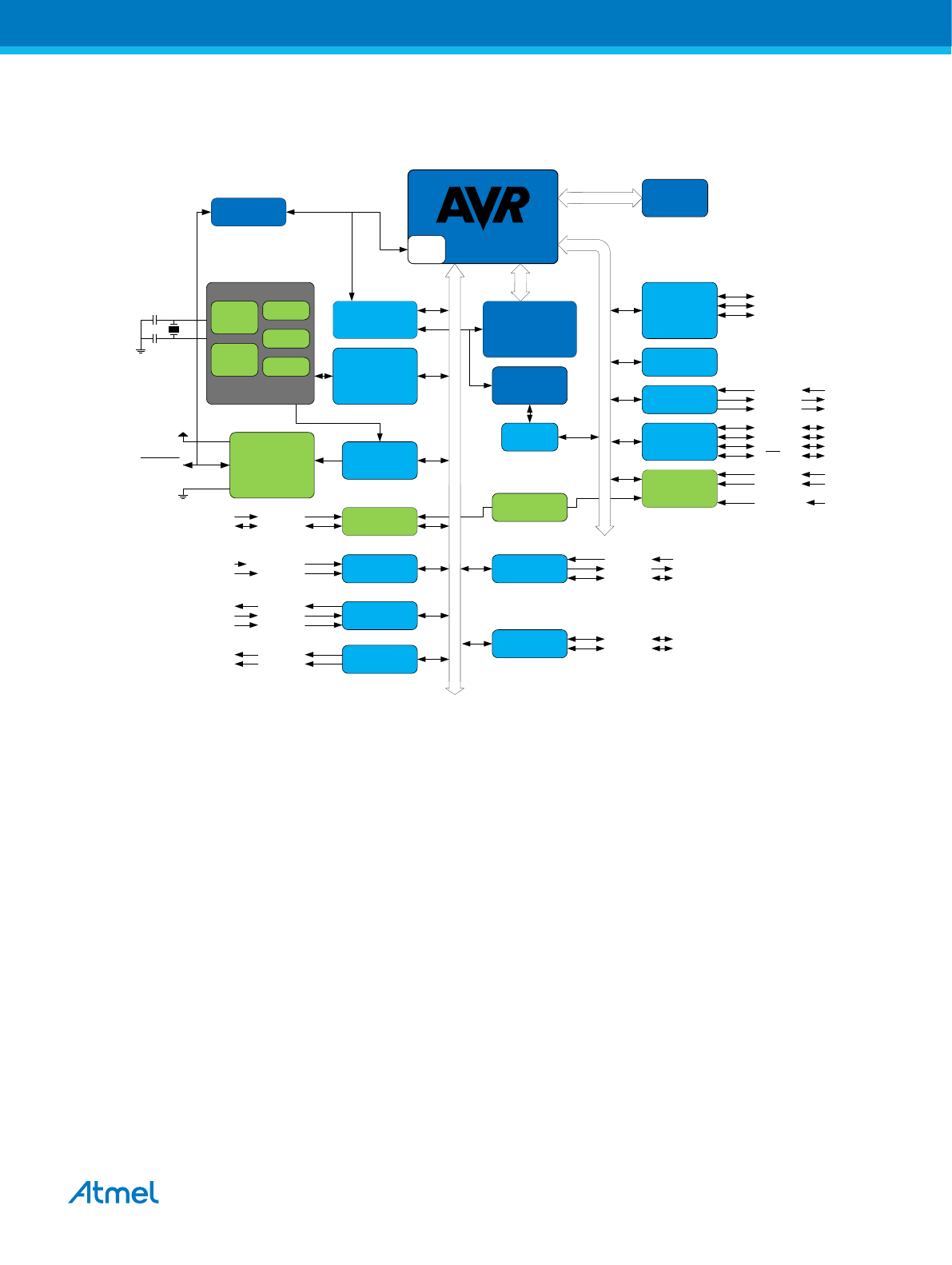
4. Block Diagram
Figure 4-1. Block Diagram
CPU
USART 0
ADC
ADC[7:0]
AREF
RxD0
TxD0
XCK0
I/O
PORTS
D
A
T
A
B
U
S
GPIOR[2:0]
SRAM
OCD
EXTINT
FLASH
NVM
programming
debugWire
I
N
/
O
U
T
D
A
T
A
B
U
S
TC 0
(8-bit)
SPI 0
AC
AIN0
AIN1
ADCMUX
EEPROM
EEPROMIF
TC 1
(16-bit)
OC1A/B
T1
ICP1
TC 2
(8-bit async)
TWI 0
SDA0
SCL0
Internal
Reference
Watchdog
Timer
Power
management
and clock
control
VCC
GND
Clock generation
8MHz
Calib RC
128kHz int
osc
32.768kHz
XOSC
External
clock
Power
Supervision
POR/BOD &
RESET
XTAL2 /
TOSC2
RESET
XTAL1 /
TOSC1
16MHz LP
XOSC
PCINT[23:0]
INT[1:0]
T0
OC0A
OC0B
MISO0
MOSI0
SCK0
SS0
OC2A
OC2B
PB[7:0]
PC[6:0]
PD[7:0]
ADC6,ADC7,PC[5:0]
AREF
PD[7:0], PC[6:0], PB[7:0]
PD3, PD2
PB1, PB2
PD5
PB0
PB3
PD3
PD4
PD6
PD5
PB4
PB3
PB5
PB2
PD6
PD7
ADC6, ADC7
PC[5:0]
PD0
PD1
PD4
PC4
PC5
Atmel ATmega328/P [DATASHEET]
Atmel-42735B-ATmega328/P_Datasheet_Complete-11/2016
13
Page 14
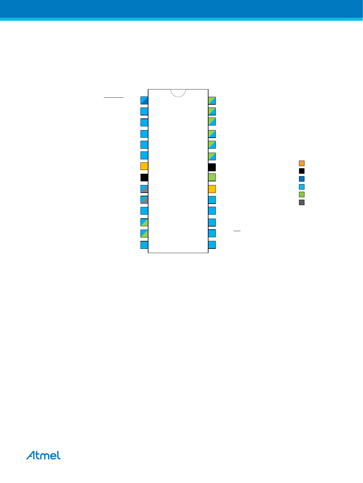
5. Pin Configurations
5.1. Pin-out
Figure 5-1. 28-pin PDIP
Power
Ground
Programming/debug
Digital
Analog
Crystal/Osc
(PCINT14/RESET) PC6
(PCINT16/RXD) PD0
(PCINT17/TXD) PD1
(PCINT18/INT0) PD2
(PCINT19/OC2B/INT1) PD3
(PCINT20/XCK/T0) PD4
VCC
GND
(PCINT6/XTAL1/TOSC1) PB6
(PCINT7/XTAL2/TOSC2) PB7
(PCINT21/OC0B/T1) PD5
(PCINT22/OC0A/AIN0) PD6
(PCINT23/AIN1) PD7
(PCINT0/CLKO/ICP1) PB0
PC5 (ADC5/SCL/PCINT13)
PC4 (ADC4/SDA/PCINT12)
PC3 (ADC3/PCINT11)
PC2 (ADC2/PCINT10)
PC1 (ADC1/PCINT9)
PC0 (ADC0/PCINT8)
GND
AREF
AVCC
PB5 (SCK/PCINT5)
PB4 (MISO/PCINT4)
PB3 (MOSI/OC2A/PCINT3)
PB2 (SS/OC1B/PCINT2)
PB1 (OC1A/PCINT1)
1
2
3
4
5
6
7
8
9
10
11
12
13
14
28
27
26
25
24
23
22
21
20
19
18
17
16
15
Atmel ATmega328/P [DATASHEET]
Atmel-42735B-ATmega328/P_Datasheet_Complete-11/2016
14
Page 15
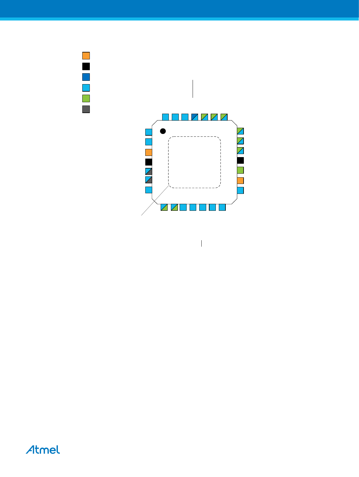
Figure 5-2. 28-pin MLF Top View
1
2
3
4
5
6
7
8
9
10
11
12
13
14
PD2 (INT0/PCINT18)
PD1 (TXD/PCINT17)
PD0 (RXD/PCINT16)
PC6 (RESET/PCINT14)
PC5 (ADC5/SCL/PCINT13)
PC4 (ADC4/SDA/PCINT12)
PC3 (ADC3/PCINT11)
PC2 (ADC2/PCINT10)
PC1 (ADC1/PCINT9)
PC0 (ADC0/PCINT8)
GND
AREF
AVCC
PB5 (SCK/PCINT5)
(PCINT22/OC0A/AIN0) PD6
(PCINT23/AIN1) PD7
(PCINT0/CLKO/ICP1) PB0
(PCINT1/OC1A) PB1
(PCINT2/SS/OC1B) PB2
(PCINT3/OC2A/MOSI) PB3
(PCINT4/MISO) PB4
(PCINT19/OC2B/INT1) PD3
(PCINT20/XCK/T0) PD4
VCC
GND
(PCINT6/XTAL1/TOSC1) PB6
(PCINT7/XTAL2/TOSC2) PB7
(PCINT21/OC0B/T1) PD5
Bottom pad should be
soldered to ground
Power
Ground
Programming/debug
Digital
Analog
Crystal/CLK
21
20
19
18
17
16
15
28
27
26
25
24
23
22
Atmel ATmega328/P [DATASHEET]
Atmel-42735B-ATmega328/P_Datasheet_Complete-11/2016
15
Page 16
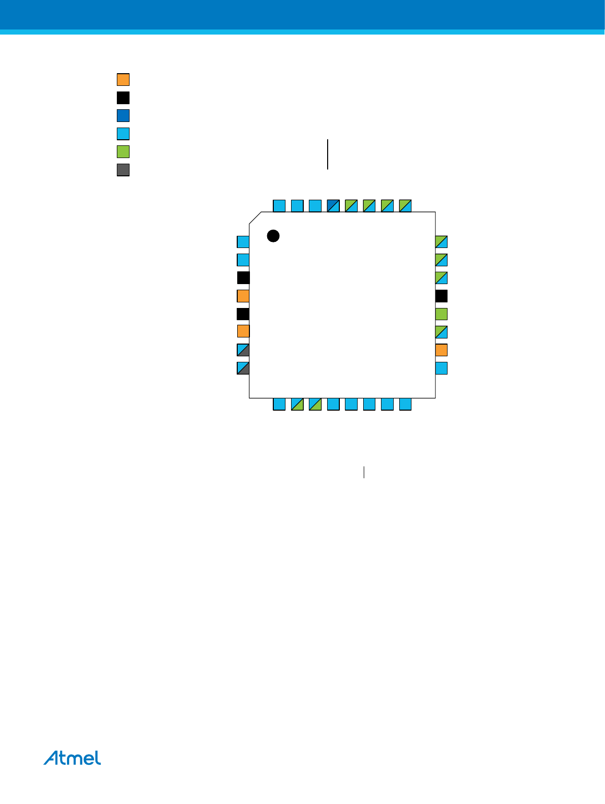
Figure 5-3. 32-pin TQFP Top View
1
2
3
4
32
31
30
29
28
27
26
5
6
7
8
24
23
22
21
20
19
18
17
25
9
10
11
12
13
14
15
16
Power
Ground
Programming/debug
Digital
Analog
Crystal/CLK
(PCINT19/OC2B/INT1) PD3
(PCINT20/XCK/T0) PD4
GND
VCC
GND
VCC
(PCINT6/XTAL1/TOSC1) PB6
(PCINT7/XTAL2/TOSC2) PB7
PD2 (INT0/PCINT18)
PD1 (TXD/PCINT17)
PD0 (RXD/PCINT16)
PC6 (RESET/PCINT14)
PC5 (ADC5/SCL/PCINT13)
PC4 (ADC4/SDA/PCINT12)
PC3 (ADC3/PCINT11)
PC2 (ADC2/PCINT10)
PC1 (ADC1/PCINT9)
PC0 (ADC0/PCINT8)
ADC7
GND
AREF
ADC6
AVCC
PB5 (SCK/PCINT5)
(PCINT21/OC0B/T1) PD5
(PCINT23/AIN1) PD7
(PCINT0/CLKO/ICP1) PB0
(PCINT1/OC1A) PB1
(PCINT2/SS/OC1B) PB2
(PCINT3/OC2A/MOSI) PB3
(PCINT4/MISO) PB4
Atmel ATmega328/P [DATASHEET]
Atmel-42735B-ATmega328/P_Datasheet_Complete-11/2016
16
Page 17
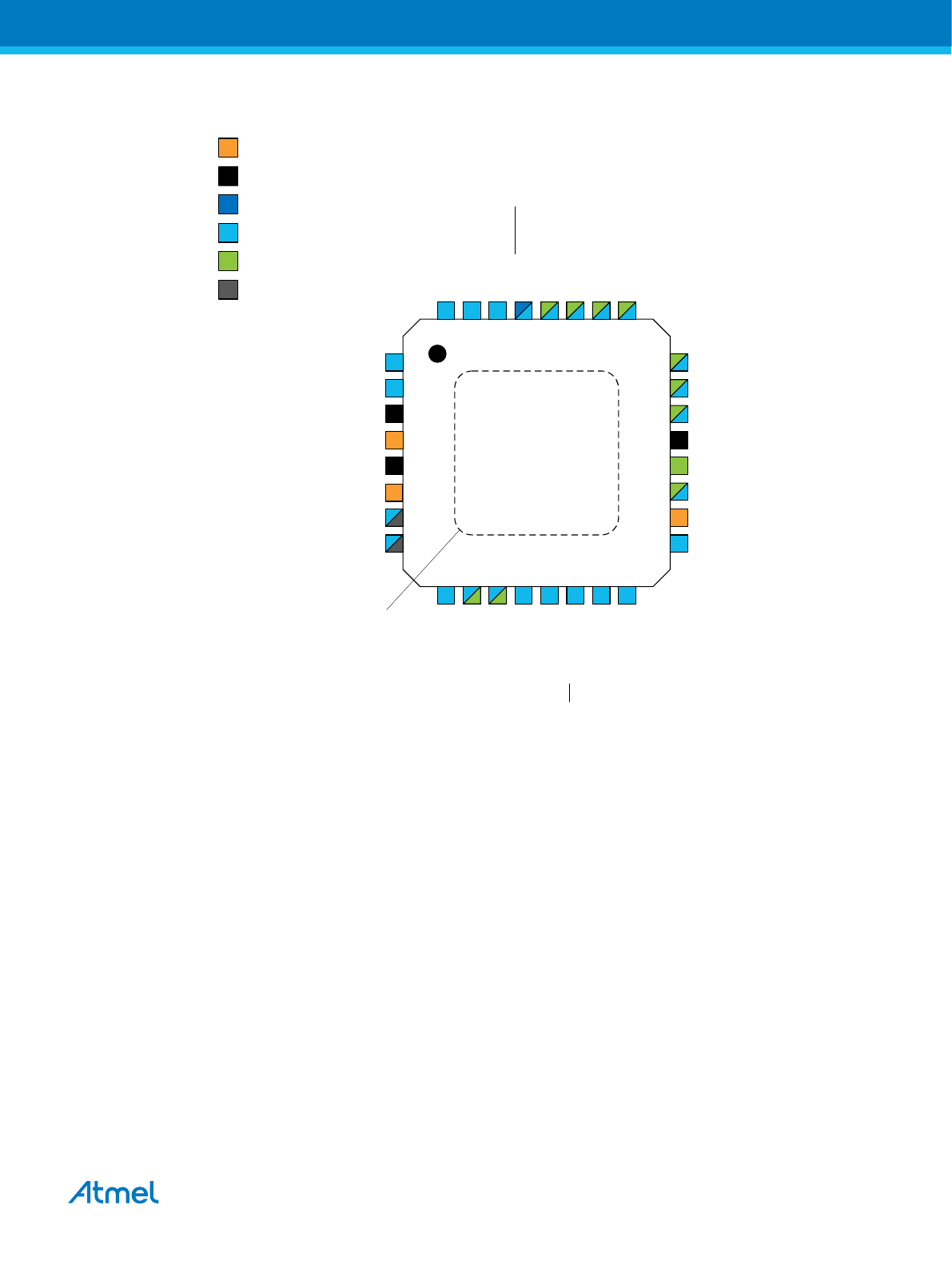
Figure 5-4. 32-pin MLF Top View
1
2
3
4
32
31
30
29
28
27
26
5
6
7
8
24
23
22
21
20
19
18
17
25
9
10
11
12
13
14
15
16
PD2 (INT0/PCINT18)
PD1 (TXD/PCINT17)
PD0 (RXD/PCINT16)
PC6 (RESET/PCINT14)
PC5 (ADC5/SCL/PCINT13)
PC4 (ADC4/SDA/PCINT12)
PC3 (ADC3/PCINT11)
PC2 (ADC2/PCINT10)
PC1 (ADC1/PCINT9)
PC0 (ADC0/PCINT8)
ADC7
GND
AREF
ADC6
AVCC
PB5 (SCK/PCINT5)
(PCINT21/OC0B/T1) PD5
(PCINT22/OC0A/AIN0) PD6
(PCINT23/AIN1) PD7
(PCINT0/CLKO/ICP1) PB0
(PCINT1/OC1A) PB1
(PCINT2/SS/OC1B) PB2
(PCINT3/OC2A/MOSI) PB3
(PCINT4/MISO) PB4
(PCINT19/OC2B/INT1) PD3
(PCINT20/XCK/T0) PD4
GND
VCC
GND
VCC
Bottom pad should be
soldered to ground
Power
Ground
Programming/debug
Digital
Analog
Crystal/CLK
5.2. Pin Descriptions
5.2.1. VCC
Digital supply voltage.
5.2.2. GND
Ground.
5.2.3. Port B (PB[7:0]) XTAL1/XTAL2/TOSC1/TOSC2
Port B is an 8-bit bi-directional I/O port with internal pull-up resistors (selected for each bit). The Port B
output buffers have symmetrical drive characteristics with both high sink and source capability. As inputs,
Port B pins that are externally pulled low will source current if the pull-up resistors are activated. The Port
B pins are tri-stated when a reset condition becomes active, even if the clock is not running.
Depending on the clock selection fuse settings, PB6 can be used as input to the inverting Oscillator
amplifier and input to the internal clock operating circuit.
Atmel ATmega328/P [DATASHEET]
Atmel-42735B-ATmega328/P_Datasheet_Complete-11/2016
17
Page 18

Depending on the clock selection fuse settings, PB7 can be used as output from the inverting Oscillator
amplifier.
If the Internal Calibrated RC Oscillator is used as chip clock source, PB[7:6] is used as TOSC[2:1] input
for the Asynchronous Timer/Counter2 if the AS2 bit in ASSR is set.
5.2.4. Port C (PC[5:0])
Port C is a 7-bit bi-directional I/O port with internal pull-up resistors (selected for each bit). The PC[5:0]
output buffers have symmetrical drive characteristics with both high sink and source capability. As inputs,
Port C pins that are externally pulled low will source current if the pull-up resistors are activated. The Port
C pins are tri-stated when a reset condition becomes active, even if the clock is not running.
5.2.5. PC6/RESET
If the RSTDISBL Fuse is programmed, PC6 is used as an I/O pin. Note that the electrical characteristics
of PC6 differ from those of the other pins of Port C.
If the RSTDISBL Fuse is unprogrammed, PC6 is used as a Reset input. A low level on this pin for longer
than the minimum pulse length will generate a Reset, even if the clock is not running. Shorter pulses are
not guaranteed to generate a Reset.
The various special features of Port C are elaborated in the Alternate Functions of Port C section.
5.2.6. Port D (PD[7:0])
Port D is an 8-bit bi-directional I/O port with internal pull-up resistors (selected for each bit). The Port D
output buffers have symmetrical drive characteristics with both high sink and source capability. As inputs,
Port D pins that are externally pulled low will source current if the pull-up resistors are activated. The Port
D pins are tri-stated when a reset condition becomes active, even if the clock is not running.
5.2.7. AV
CC
AV
CC
is the supply voltage pin for the A/D Converter, PC[3:0], and PE[3:2]. It should be externally
connected to V
CC
, even if the ADC is not used. If the ADC is used, it should be connected to V
CC
through
a low-pass filter. Note that PC[6:4] use digital supply voltage, V
CC
.
5.2.8. AREF
AREF is the analog reference pin for the A/D Converter.
5.2.9. ADC[7:6] (TQFP and VFQFN Package Only)
In the TQFP and VFQFN package, ADC[7:6] serve as analog inputs to the A/D converter. These pins are
powered from the analog supply and serve as 10-bit ADC channels.
Atmel ATmega328/P [DATASHEET]
Atmel-42735B-ATmega328/P_Datasheet_Complete-11/2016
18
Page 19
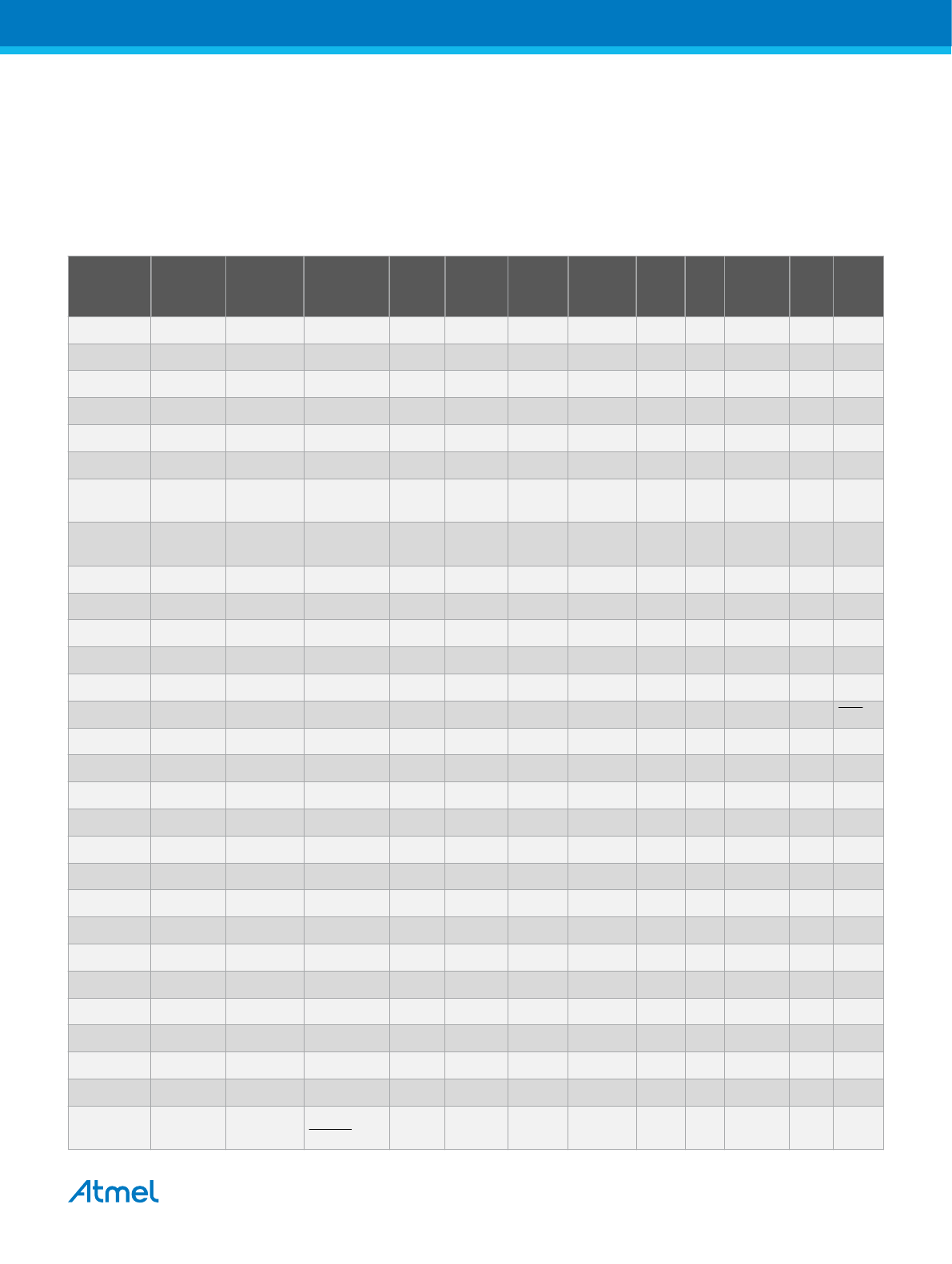
6. I/O Multiplexing
Each pin is by default controlled by the PORT as a general purpose I/O and alternatively it can be
assigned to one of the peripheral functions.
The following table describes the peripheral signals multiplexed to the PORT I/O pins.
Table 6-1. PORT Function Multiplexing
(32-pin
MLF/TQFP)
Pin#
(28-pin
MLF) Pin#
(28-pin
PIPD) Pin#
PAD EXTINT PCINT ADC/AC OSC T/C #0 T/C
#1
USART 0 I2C 0 SPI 0
1 1 5 PD[3] INT1 PCINT19 OC2B
2 2 6 PD[4] PCINT20 T0 XCK0
4 3 7 VCC
3 4 8 GND
6 - - VCC
5 - - GND
7 5 9 PB[6] PCINT6 XTAL1/
TOSC1
8 6 10 PB[7] PCINT7 XTAL2/
TOSC2
9 7 11 PD[5] PCINT21 OC0B T1
10 8 12 PD[6] PCINT22 AIN0 OC0A
11 9 13 PD[7] PCINT23 AIN1
12 10 14 PB[0] PCINT0 CLKO ICP1
13 11 15 PB[1] PCINT1 OC1A
14 12 16 PB[2] PCINT2 OC1B SS0
15 13 17 PB[3] PCINT3 OC2A MOSI0
16 14 18 PB[4] PCINT4 MISO0
17 15 19 PB[5] PCINT5 SCK0
18 16 20 AVCC
19 - - ADC6 ADC6
20 17 21 AREF
21 18 22 GND
22 - - ADC7 ADC7
23 19 13 PC[0] PCINT8 ADC0
24 20 24 PC[1] PCINT9 ADC1
25 21 25 PC[2] PCINT10 ADC2
26 22 26 PC[3] PCINT11 ADC3
27 23 27 PC[4] PCINT12 ADC4 SDA0
28 24 28 PC[5] PCINT13 ADC5 SCL0
29 25 1 PC[6]/
RESET
PCINT14
Atmel ATmega328/P [DATASHEET]
Atmel-42735B-ATmega328/P_Datasheet_Complete-11/2016
19
Page 20

(32-pin
MLF/TQFP)
Pin#
(28-pin
MLF) Pin#
(28-pin
PIPD) Pin#
PAD EXTINT PCINT ADC/AC OSC T/C #0 T/C
#1
USART 0 I2C 0 SPI 0
30 26 2 PD[0] PCINT16 RXD0
31 27 3 PD[1] PCINT17 TXD0
32 28 4 PD[2] INT0 PCINT18
Atmel ATmega328/P [DATASHEET]
Atmel-42735B-ATmega328/P_Datasheet_Complete-11/2016
20
Page 21

7. Resources
A comprehensive set of development tools, application notes, and datasheets are available for download
on http://www.atmel.com/avr.
Atmel ATmega328/P [DATASHEET]
Atmel-42735B-ATmega328/P_Datasheet_Complete-11/2016
21
Page 22

8. Data Retention
Reliability Qualification results show that the projected data retention failure rate is much less than 1 PPM
over 20 years at 85°C or 100 years at 25°C.
Atmel ATmega328/P [DATASHEET]
Atmel-42735B-ATmega328/P_Datasheet_Complete-11/2016
22
Page 23

9. About Code Examples
This documentation contains simple code examples that briefly show how to use various parts of the
device. These code examples assume that the part specific header file is included before compilation. Be
aware that not all C compiler vendors include bit definitions in the header files and interrupt handling in C
is compiler dependent. Confirm with the C compiler documentation for more details.
For I/O Registers located in extended I/O map, “IN”, “OUT”, “SBIS”, “SBIC”, “CBI”, and “SBI” instructions
must be replaced with instructions that allow access to extended I/O. Typically “LDS” and “STS”
combined with “SBRS”, “SBRC”, “SBR”, and “CBR”.
Atmel ATmega328/P [DATASHEET]
Atmel-42735B-ATmega328/P_Datasheet_Complete-11/2016
23
Page 24

10. Capacitive Touch Sensing
10.1. QTouch Library
The Atmel
®
QTouch
®
Library provides a simple to use solution to realize touch sensitive interfaces on
most Atmel AVR
®
microcontrollers. The QTouch Library includes support for the Atmel QTouch and Atmel
QMatrix
®
acquisition methods.
Touch sensing can be added to any application by linking the appropriate Atmel QTouch Library for the
AVR Microcontroller. This is done by using a simple set of APIs to define the touch channels and sensors,
and then calling the touch sensing API’s to retrieve the channel information and determine the touch
sensor states.
The QTouch Library is FREE and downloadable from the Atmel website at the following location: http://
www.atmel.com/technologies/touch/. For implementation details and other information, refer to the Atmel
QTouch Library User Guide - also available for download from the Atmel website.
Atmel ATmega328/P [DATASHEET]
Atmel-42735B-ATmega328/P_Datasheet_Complete-11/2016
24
Page 25
11. AVR CPU Core
11.1. Overview
This section discusses the AVR core architecture in general. The main function of the CPU core is to
ensure correct program execution. The CPU must therefore be able to access memories, perform
calculations, control peripherals, and handle interrupts.
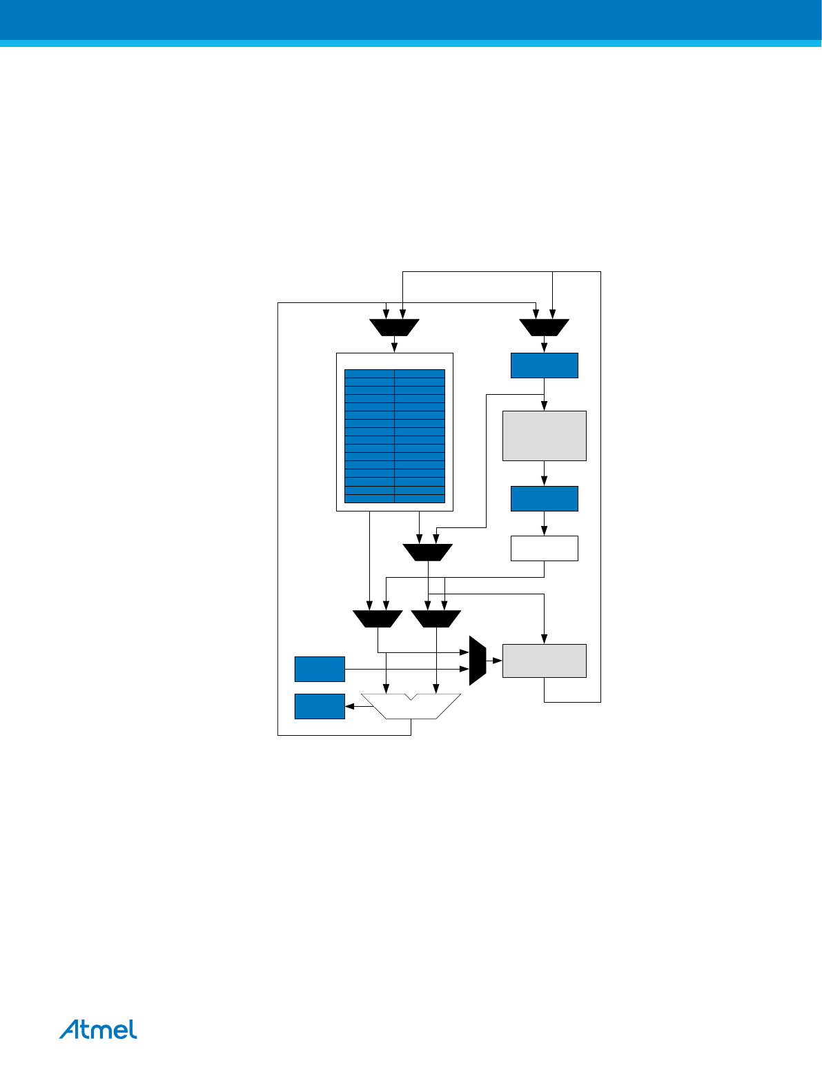
Figure 11-1. Block Diagram of the AVR Architecture
Register file
Flash program
memory
Program
counter
Instruction
register
Instruction
decode
Data memory
ALU
Status
register
R0R1
R2R3
R4R5
R6R7
R8R9
R10R11
R12R13
R14R15
R16R17
R18R19
R20R21
R22R23
R24R25
R26 (XL)R27 (XH)
R28 (YL)R29 (YH)
R30 (ZL)R31 (ZH)
Stack
pointer
In order to maximize performance and parallelism, the AVR uses a Harvard architecture – with separate
memories and buses for program and data. Instructions in the program memory are executed with a
single level pipelining. While one instruction is being executed, the next instruction is pre-fetched from the
program memory. This concept enables instructions to be executed in every clock cycle. The program
memory is In-System Reprogrammable Flash memory.
The fast-access Register File contains 32 x 8-bit general purpose working registers with a single clock
cycle access time. This allows single-cycle Arithmetic Logic Unit (ALU) operation. In a typical ALU
operation, two operands are output from the Register File, the operation is executed, and the result is
stored back in the Register File – in one clock cycle.
Six of the 32 registers can be used as three 16-bit indirect address register pointers for Data Space
addressing – enabling efficient address calculations. One of the these address pointers can also be used
as an address pointer for look up tables in Flash program memory. These added function registers are
the 16-bit X-, Y-, and Z-register, described later in this section.
Atmel ATmega328/P [DATASHEET]
Atmel-42735B-ATmega328/P_Datasheet_Complete-11/2016
25
Page 26

The ALU supports arithmetic and logic operations between registers or between a constant and a
register. Single register operations can also be executed in the ALU. After an arithmetic operation, the
Status Register is updated to reflect information about the result of the operation.
Program flow is provided by conditional and unconditional jump and call instructions, able to directly
address the whole address space. Most AVR instructions have a single 16-bit word format. Every
program memory address contains a 16- or 32-bit instruction.
Program Flash memory space is divided in two sections, the Boot Program section and the Application
Program section. Both sections have dedicated Lock bits for write and read/write protection. The SPM
instruction that writes into the Application Flash memory section must reside in the Boot Program section.
During interrupts and subroutine calls, the return address Program Counter (PC) is stored on the Stack.
The Stack is effectively allocated in the general data SRAM, and consequently the Stack size is only
limited by the total SRAM size and the usage of the SRAM. All user programs must initialize the SP in the
Reset routine (before subroutines or interrupts are executed). The Stack Pointer (SP) is read/write
accessible in the I/O space. The data SRAM can easily be accessed through the five different addressing
modes supported in the AVR architecture.
The memory spaces in the AVR architecture are all linear and regular memory maps.
A flexible interrupt module has its control registers in the I/O space with an additional Global Interrupt
Enable bit in the Status Register. All interrupts have a separate Interrupt Vector in the Interrupt Vector
table. The interrupts have priority in accordance with their Interrupt Vector position. The lower the
Interrupt Vector address, the higher the priority.
The I/O memory space contains 64 addresses for CPU peripheral functions as Control Registers, SPI,
and other I/O functions. The I/O Memory can be accessed directly, or as the Data Space locations
following those of the Register File, 0x20 - 0x5F. In addition, this device has Extended I/O space from
0x60 - 0xFF in SRAM where only the ST/STS/STD and LD/LDS/LDD instructions can be used.
11.2. ALU – Arithmetic Logic Unit
The high-performance AVR ALU operates in direct connection with all the 32 general purpose working
registers. Within a single clock cycle, arithmetic operations between general purpose registers or between
a register and an immediate are executed. The ALU operations are divided into three main categories –
arithmetic, logical, and bit-functions. Some implementations of the architecture also provide a powerful
multiplier supporting both signed/unsigned multiplication and fractional format. See Instruction Set
Summary section for a detailed description.
Related Links
Instruction Set Summary on page 432
11.3. Status Register
The Status Register contains information about the result of the most recently executed arithmetic
instruction. This information can be used for altering program flow in order to perform conditional
operations. The Status Register is updated after all ALU operations, as specified in the Instruction Set
Reference. This will in many cases remove the need for using the dedicated compare instructions,
resulting in faster and more compact code.
The Status Register is not automatically stored when entering an interrupt routine and restored when
returning from an interrupt. This must be handled by software.
Atmel ATmega328/P [DATASHEET]
Atmel-42735B-ATmega328/P_Datasheet_Complete-11/2016
26
Page 27

11.3.1. Status Register
When addressing I/O Registers as data space using LD and ST instructions, the provided offset must be
used. When using the I/O specific commands IN and OUT, the offset is reduced by 0x20, resulting in an
I/O address offset within 0x00 - 0x3F.
Name: SREG
Offset: 0x5F
Reset: 0x00
Property:
When addressing as I/O Register: address offset is 0x3F
Bit 7 6 5 4 3 2 1 0
I T H S V N Z C
Access
R/W R/W R/W R/W R/W R/W R/W R/W
Reset 0 0 0 0 0 0 0 0
Bit 7 – I: Global Interrupt Enable
The Global Interrupt Enable bit must be set for the interrupts to be enabled. The individual interrupt
enable control is then performed in separate control registers. If the Global Interrupt Enable Register is
cleared, none of the interrupts are enabled independent of the individual interrupt enable settings. The I-
bit is cleared by hardware after an interrupt has occurred, and is set by the RETI instruction to enable
subsequent interrupts. The I-bit can also be set and cleared by the application with the SEI and CLI
instructions, as described in the instruction set reference.
Bit 6 – T: Copy Storage
The Bit Copy instructions BLD (Bit LoaD) and BST (Bit STore) use the T-bit as source or destination for
the operated bit. A bit from a register in the Register File can be copied into T by the BST instruction, and
a bit in T can be copied into a bit in a register in the Register File by the BLD instruction.
Bit 5 – H: Half Carry Flag
The Half Carry Flag H indicates a Half Carry in some arithmetic operations. Half Carry Flag is useful in
BCD arithmetic. See the Instruction Set Description for detailed information.
Bit 4 – S: Sign Flag, S = N ㊉ V
The S-bit is always an exclusive or between the Negative Flag N and the Two’s Complement Overflow
Flag V. See the Instruction Set Description for detailed information.
Bit 3 – V: Two’s Complement Overflow Flag
The Two’s Complement Overflow Flag V supports two’s complement arithmetic. See the Instruction Set
Description for detailed information.
Bit 2 – N: Negative Flag
The Negative Flag N indicates a negative result in an arithmetic or logic operation. See the Instruction Set
Description for detailed information.
Bit 1 – Z: Zero Flag
The Zero Flag Z indicates a zero result in an arithmetic or logic operation. See the Instruction Set
Description for detailed information.
Atmel ATmega328/P [DATASHEET]
Atmel-42735B-ATmega328/P_Datasheet_Complete-11/2016
27
Page 28
Bit 0 – C: Carry Flag
The Carry Flag C indicates a carry in an arithmetic or logic operation. See the Instruction Set Description
for detailed information.
11.4. General Purpose Register File
The Register File is optimized for the AVR Enhanced RISC instruction set. In order to achieve the
required performance and flexibility, the following input/output schemes are supported by the Register
File:
• One 8-bit output operand and one 8-bit result input
• Two 8-bit output operands and one 8-bit result input
• Two 8-bit output operands and one 16-bit result input
• One 16-bit output operand and one 16-bit result input
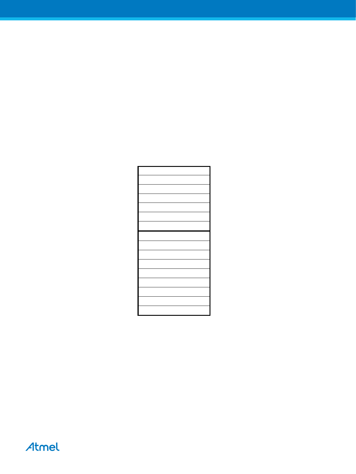
Figure 11-2. AVR CPU General Purpose Working Registers
7
0
Addr.
R0
0x0 0
R1
0x0 1
R2
0x0 2
…
R13
0x0D
Ge nera l
R14
0x0E
P urpos e
R15
0x0 F
Working
R16
0x1 0
Re giste rs
R17
0x1 1
…
R26
0x1A
X-reg iste r Low Byte
R27
0x1B
X-reg iste r High Byte
R28
0x1C
Y-reg iste r Low Byte
R29
0x1D
Y-reg iste r High Byte
R30
0x1E
Z-regis te r Low Byte
R31
0x1 F
Z-regis te r High Byte
Most of the instructions operating on the Register File have direct access to all registers, and most of
them are single cycle instructions. As shown in the figure, each register is also assigned a data memory
address, mapping them directly into the first 32 locations of the user Data Space. Although not being
physically implemented as SRAM locations, this memory organization provides great flexibility in access
of the registers, as the X-, Y-, and Z-pointer registers can be set to index any register in the file.
11.4.1. The X-register, Y-register, and Z-register
The registers R26...R31 have some added functions to their general purpose usage. These registers are
16-bit address pointers for indirect addressing of the data space. The three indirect address registers X,
Y, and Z are defined as described in the figure.
Atmel ATmega328/P [DATASHEET]
Atmel-42735B-ATmega328/P_Datasheet_Complete-11/2016
28
Page 29
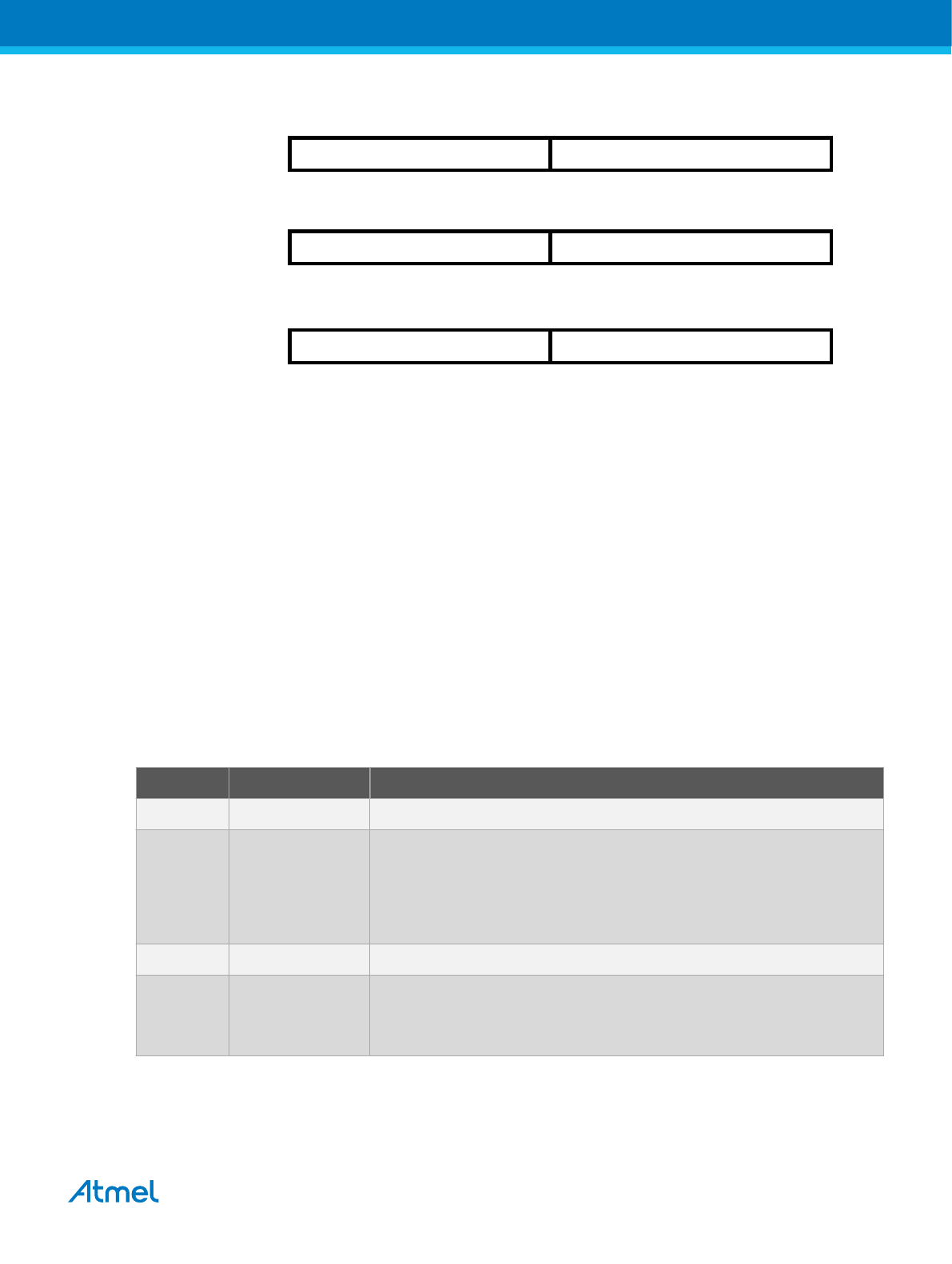
Figure 11-3. The X-, Y-, and Z-registers
15
XH
XL
0
X-register
7
0
7
0
R27
R26
15
YH
YL
0
Y-register
7
0
7
0
R29
R28
15
ZH
ZL
0
Z-register
7
0
7
0
R31
R30
In the different addressing modes these address registers have functions as fixed displacement,
automatic increment, and automatic decrement (see the instruction set reference for details).
Related Links
Instruction Set Summary on page 432
11.5. Stack Pointer
The Stack is mainly used for storing temporary data, for storing local variables and for storing return
addresses after interrupts and subroutine calls. The Stack is implemented as growing from higher to
lower memory locations. The Stack Pointer Register always points to the top of the Stack.
The Stack Pointer points to the data SRAM Stack area where the Subroutine and Interrupt Stacks are
located. A Stack PUSH command will decrease the Stack Pointer. The Stack in the data SRAM must be
defined by the program before any subroutine calls are executed or interrupts are enabled. Initial Stack
Pointer value equals the last address of the internal SRAM and the Stack Pointer must be set to point
above start of the SRAM. See the table for Stack Pointer details.
Table 11-1. Stack Pointer Instructions
Instruction Stack pointer Description
PUSH Decremented by 1 Data is pushed onto the stack
CALL
ICALL
RCALL
Decremented by 2 Return address is pushed onto the stack with a subroutine call or
interrupt
POP Incremented by 1 Data is popped from the stack
RET
RETI
Incremented by 2 Return address is popped from the stack with return from subroutine or
return from interrupt
The AVR Stack Pointer is implemented as two 8-bit registers in the I/O space. The number of bits actually
used is implementation dependent. Note that the data space in some implementations of the AVR
architecture is so small that only SPL is needed. In this case, the SPH Register will not be present.
Atmel ATmega328/P [DATASHEET]
Atmel-42735B-ATmega328/P_Datasheet_Complete-11/2016
29
Page 30
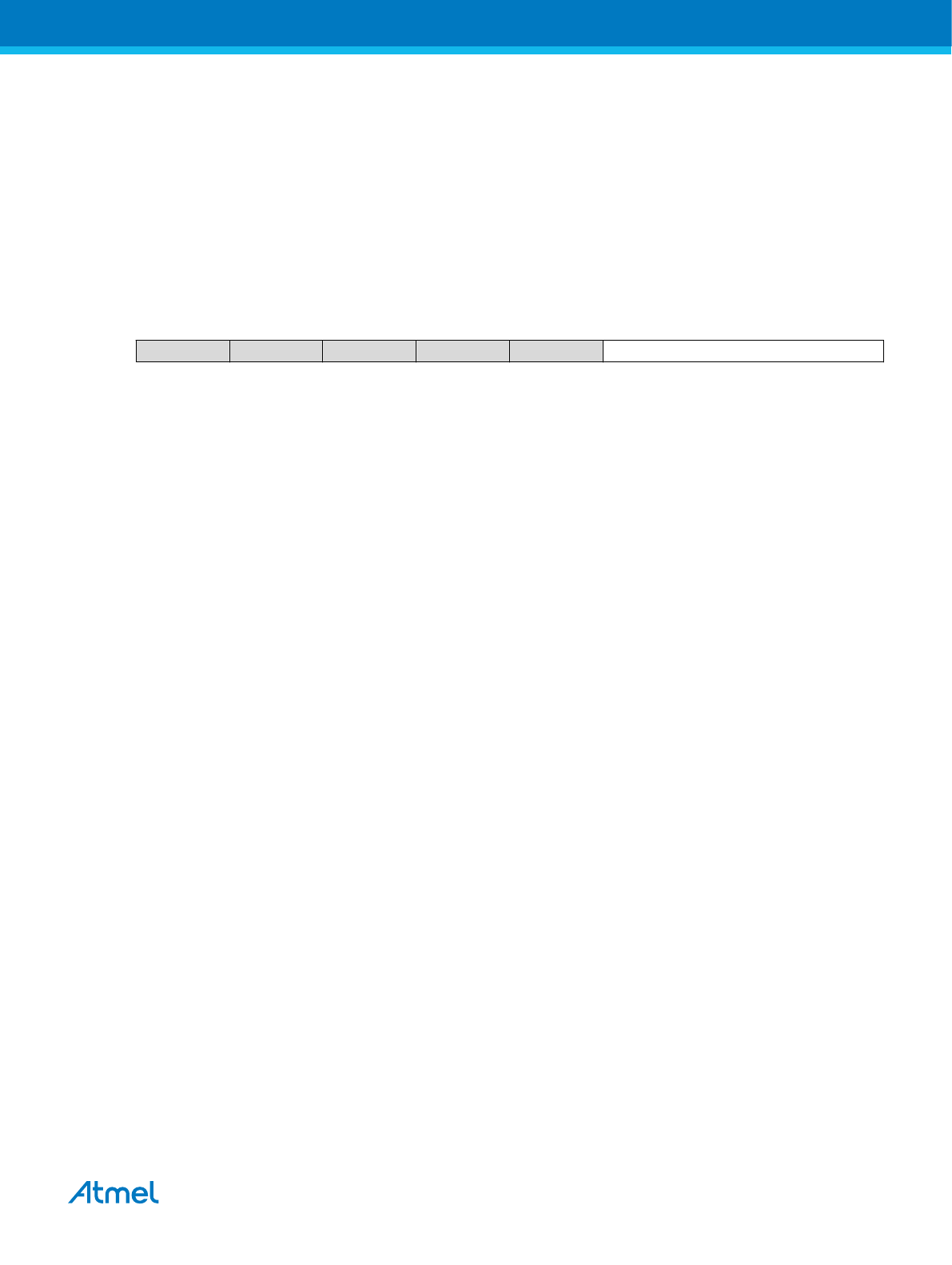
11.5.1. Stack Pointer Register High byte
When using the I/O specific commands IN and OUT, the I/O addresses 0x00 - 0x3F must be used. When
addressing I/O Registers as data space using LD and ST instructions, 0x20 must be added to these offset
addresses.
Name: SPH
Offset: 0x5E
Reset: RAMEND
Property:
When addressing I/O Registers as data space the offset address is 0x3E
Bit 7 6 5 4 3 2 1 0
(SP[10:8]) SPH
Access
RW RW RW
Reset 0 0 0
Bits 2:0 – (SP[10:8]) SPH: Stack Pointer Register
SPH and SPL are combined into SP. It means SPH[2:0] is SP[10:8].
Atmel ATmega328/P [DATASHEET]
Atmel-42735B-ATmega328/P_Datasheet_Complete-11/2016
30
Page 31
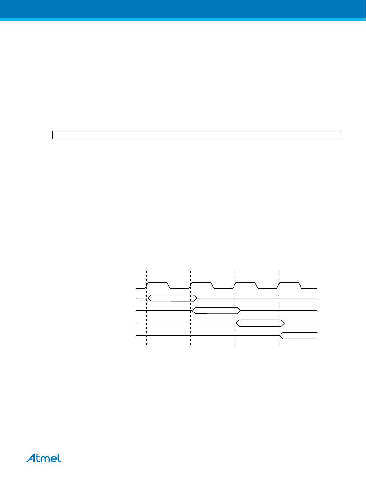
11.5.2. Stack Pointer Register Low byte
When using the I/O specific commands IN and OUT, the I/O addresses 0x00 - 0x3F must be used. When
addressing I/O Registers as data space using LD and ST instructions, 0x20 must be added to these offset
addresses.
Name: SPL
Offset: 0x5D
Reset: 0x11111111
Property:
When addressing I/O Registers as data space the offset address is 0x3D
Bit 7 6 5 4 3 2 1 0
(SP[7:0]) SPL
Access
RW RW RW RW RW RW RW RW
Reset 0 0 0 0 0 0 0 1
Bits 7:0 – (SP[7:0]) SPL: Stack Pointer Register
SPH and SPL are combined into SP. It means SPL[7:0] is SP[7:0].
11.6. Instruction Execution Timing
This section describes the general access timing concepts for instruction execution. The AVR CPU is
driven by the CPU clock clk
CPU
, directly generated from the selected clock source for the chip. No internal
clock division is used. The Figure below shows the parallel instruction fetches and instruction executions
enabled by the Harvard architecture and the fast-access Register File concept. This is the basic pipelining
concept to obtain up to 1 MIPS per MHz with the corresponding unique results for functions per cost,
functions per clocks, and functions per power-unit.
Figure 11-4. The Parallel Instruction Fetches and Instruction Executions
clk
1st Instruction Fetch
1st Instruction Execute
2nd Instruction Fetch
2nd Instruction Execute
3rd Instruction Fetch
3rd Instruction Execute
4th Instruction Fetch
T1 T2 T3 T4
CPU
The following Figure shows the internal timing concept for the Register File. In a single clock cycle an
ALU operation using two register operands is executed, and the result is stored back to the destination
register.
Atmel ATmega328/P [DATASHEET]
Atmel-42735B-ATmega328/P_Datasheet_Complete-11/2016
31
Page 32
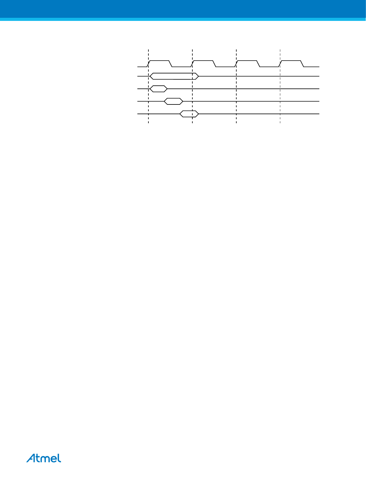
Figure 11-5. Single Cycle ALU Operation
Total Execution Time
Register Operands Fetch
ALU Operation Execute
Result Write Back
T1 T2 T3 T4
clk
CPU
11.7. Reset and Interrupt Handling
The AVR provides several different interrupt sources. These interrupts and the separate Reset Vector
each have a separate program vector in the program memory space. All interrupts are assigned individual
enable bits which must be written logic one together with the Global Interrupt Enable bit in the Status
Register in order to enable the interrupt. Depending on the Program Counter value, interrupts may be
automatically disabled when Boot Lock bits BLB02 or BLB12 are programmed. This feature improves
software security.
The lowest addresses in the program memory space are by default defined as the Reset and Interrupt
Vectors. They have determined priority levels: The lower the address the higher is the priority level.
RESET has the highest priority, and next is INT0 – the External Interrupt Request 0. The Interrupt Vectors
can be moved to the start of the Boot Flash section by setting the IVSEL bit in the MCU Control Register
(MCUCR). The Reset Vector can also be moved to the start of the Boot Flash section by programming
the BOOTRST Fuse.
When an interrupt occurs, the Global Interrupt Enable I-bit is cleared and all interrupts are disabled. The
user software can write logic one to the I-bit to enable nested interrupts. All enabled interrupts can then
interrupt the current interrupt routine. The I-bit is automatically set when a Return from Interrupt
instruction – RETI – is executed.
There are basically two types of interrupts:
The first type is triggered by an event that sets the Interrupt Flag. For these interrupts, the Program
Counter is vectored to the actual Interrupt Vector in order to execute the interrupt handling routine, and
hardware clears the corresponding Interrupt Flag. Interrupt Flags can also be cleared by writing a logic
one to the flag bit position(s) to be cleared. If an interrupt condition occurs while the corresponding
interrupt enable bit is cleared, the Interrupt Flag will be set and remembered until the interrupt is enabled,
or the flag is cleared by software. Similarly, if one or more interrupt conditions occur while the Global
Interrupt Enable bit is cleared, the corresponding Interrupt Flag(s) will be set and remembered until the
Global Interrupt Enable bit is set, and will then be executed by order of priority.
The second type of interrupts will trigger as long as the interrupt condition is present. These interrupts do
not necessarily have Interrupt Flags. If the interrupt condition disappears before the interrupt is enabled,
the interrupt will not be triggered. When the AVR exits from an interrupt, it will always return to the main
program and execute one more instruction before any pending interrupt is served.
The Status Register is not automatically stored when entering an interrupt routine, nor restored when
returning from an interrupt routine. This must be handled by software.
When using the CLI instruction to disable interrupts, the interrupts will be immediately disabled. No
interrupt will be executed after the CLI instruction, even if it occurs simultaneously with the CLI instruction.
Atmel ATmega328/P [DATASHEET]
Atmel-42735B-ATmega328/P_Datasheet_Complete-11/2016
32
Page 33

The following example shows how this can be used to avoid interrupts during the timed EEPROM write
sequence.
Assembly Code Example
in r16, SREG ; store SREG value
cli ; disable interrupts during timed sequence
sbi EECR, EEMPE ; start EEPROM write
sbi EECR, EEPE
out SREG, r16 ; restore SREG value (I-bit)
C Code Example
char cSREG;
cSREG = SREG; /* store SREG value */
/* disable interrupts during timed sequence */
_CLI();
EECR |= (1<<EEMPE); /* start EEPROM write */
EECR |= (1<<EEPE);
SREG = cSREG; /* restore SREG value (I-bit) */
Note: Please refer to About Code Examples.
When using the SEI instruction to enable interrupts, the instruction following SEI will be executed before
any pending interrupts, as shown in this example.
Assembly Code Example
sei ; set Global Interrupt Enable
sleep ; enter sleep, waiting for interrupt
; note: will enter sleep before any pending interrupt(s)
C Code Example
__enable_interrupt(); /* set Global Interrupt Enable */
__sleep(); /* enter sleep, waiting for interrupt */
/* note: will enter sleep before any pending interrupt(s) */
Note: Please refer to About Code Examples.
Related Links
Memory Programming on page 347
Boot Loader Support – Read-While-Write Self-Programming on page 330
11.7.1. Interrupt Response Time
The interrupt execution response for all the enabled AVR interrupts is four clock cycles minimum. After
four clock cycles the program vector address for the actual interrupt handling routine is executed. During
this four clock cycle period, the Program Counter is pushed onto the Stack. The vector is normally a jump
to the interrupt routine, and this jump takes three clock cycles. If an interrupt occurs during execution of a
multi-cycle instruction, this instruction is completed before the interrupt is served. If an interrupt occurs
when the MCU is in sleep mode, the interrupt execution response time is increased by four clock cycles.
This increase comes in addition to the start-up time from the selected sleep mode. A return from an
interrupt handling routine takes four clock cycles. During these four clock cycles, the Program Counter
(two bytes) is popped back from the Stack, the Stack Pointer is incremented by two, and the I-bit in SREG
is set.
Atmel ATmega328/P [DATASHEET]
Atmel-42735B-ATmega328/P_Datasheet_Complete-11/2016
33
Page 34

12. AVR Memories
12.1. Overview
This section describes the different memory types in the device. The AVR architecture has two main
memory spaces, the Data Memory and the Program Memory space. In addition, the device features an
EEPROM Memory for data storage. All memory spaces are linear and regular.
12.2. In-System Reprogrammable Flash Program Memory
The ATmega328/P contains 32Kbytes On-chip In-System Reprogrammable Flash memory for program
storage. Since all AVR instructions are 16 or 32 bits wide, the Flash is organized as 16K x 16. For
software security, the Flash Program memory space is divided into two sections - Boot Loader Section
and Application Program Section in the device .
The Flash memory has an endurance of at least 10,000 write/erase cycles. The ATmega328/P Program
Counter (PC) is 14 bits wide, thus addressing the 16K program memory locations. The operation of Boot
Program section and associated Boot Lock bits for software protection are described in detail in Boot
Loader Support – Read-While-Write Self-Programming. Refer to Memory Programming for the description
on Flash data serial downloading using the SPI pins.
Constant tables can be allocated within the entire program memory address space, using the Load
Program Memory (LPM) instruction.
Timing diagrams for instruction fetch and execution are presented in Instruction Exectution Timing.
Figure 12-1. Program Memory Map ATmega328/P
0x0000
0x3FFF
Program Memory
Application Flash Section
Boot Flash Section
Related Links
BTLDR - Boot Loader Support – Read-While-Write Self-Programming on page 330
MEMPROG- Memory Programming on page 347
Instruction Execution Timing on page 31
Atmel ATmega328/P [DATASHEET]
Atmel-42735B-ATmega328/P_Datasheet_Complete-11/2016
34
Page 35
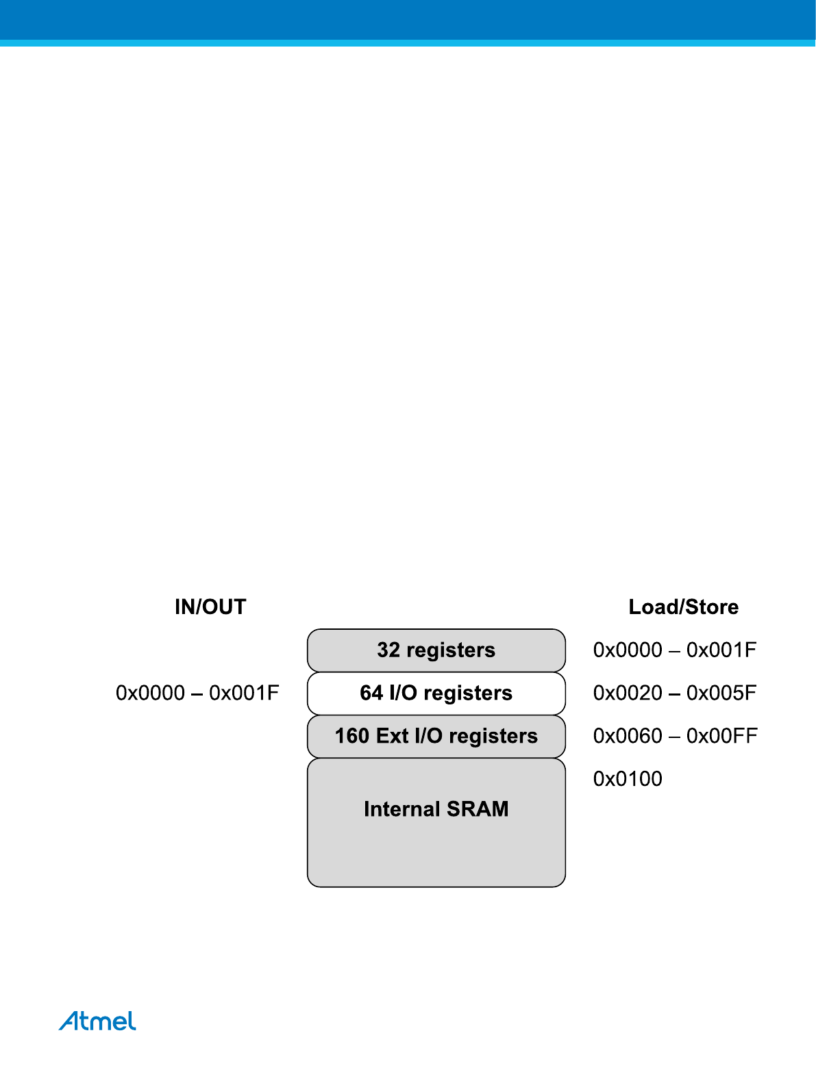
12.3. SRAM Data Memory
The following figure shows how the device SRAM Memory is organized.
The device is a complex microcontroller with more peripheral units than can be supported within the 64
locations reserved in the Opcode for the IN and OUT instructions. For the Extended I/O space from 0x60
- 0xFF in SRAM, only the ST/STS/STD and LD/LDS/LDD instructions can be used.
The lower 2303 data memory locations address both the Register File, the I/O memory, Extended I/O
memory, and the internal data SRAM. The first 32 locations address the Register File, the next 64
location the standard I/O memory, then 160 locations of Extended I/O memory, and the next 2K locations
address the internal data SRAM.
The five different addressing modes for the data memory cover:
• Direct
– The direct addressing reaches the entire data space.
• Indirect with Displacement
– The Indirect with Displacement mode reaches 63 address locations from the base address
given by the Y- or Z-register.
• Indirect
– In the Register File, registers R26 to R31 feature the indirect addressing pointer registers.
• Indirect with Pre-decrement
– The address registers X, Y, and Z are decremented.
• Indirect with Post-increment
– The address registers X, Y, and Z are incremented.
The 32 general purpose working registers, 64 I/O Registers, 160 Extended I/O Registers, and the 2K
bytes of internal data SRAM in the device are all accessible through all these addressing modes.
Figure 12-2. Data Memory Map with 2048 byte internal data SRAM
(2048x8)
0x08FF
12.3.1. Data Memory Access Times
The internal data SRAM access is performed in two clk
CPU
cycles as described in the following Figure.
Atmel ATmega328/P [DATASHEET]
Atmel-42735B-ATmega328/P_Datasheet_Complete-11/2016
35
Page 36
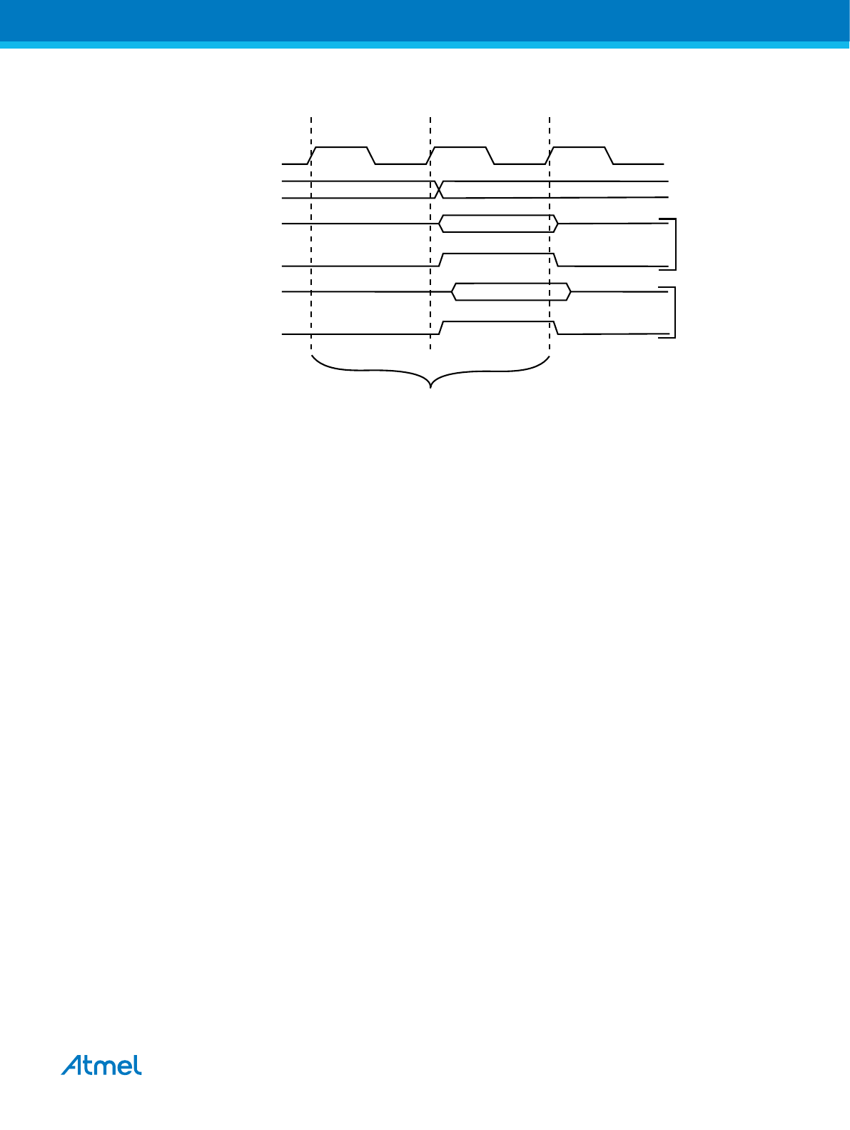
Figure 12-3. On-chip Data SRAM Access Cycles
clk
WR
RD
Data
Data
Address
Address valid
T1 T2 T3
Compute Address
Read
Write
CPU
Memory Access Instruction
Next Instruction
12.4. EEPROM Data Memory
The ATmega328/P contains 1K bytes of data EEPROM memory. It is organized as a separate data
space, in which single bytes can be read and written. The EEPROM has an endurance of at least
100,000 write/erase cycles. The access between the EEPROM and the CPU is described in the following,
specifying the EEPROM Address Registers, the EEPROM Data Register, and the EEPROM Control
Register.
See the related links for a detailed description on EEPROM Programming in SPI or Parallel Programming
mode.
Related Links
MEMPROG- Memory Programming on page 347
12.4.1. EEPROM Read/Write Access
The EEPROM Access Registers are accessible in the I/O space.
The write access time for the EEPROM is given in Table 12-2. A self-timing function, however, lets the
user software detect when the next byte can be written. If the user code contains instructions that write
the EEPROM, some precautions must be taken. In heavily filtered power supplies, V
CC
is likely to rise or
fall slowly on power-up/down. This causes the device for some period of time to run at a voltage lower
than specified as minimum for the clock frequency used. Please refer to Preventing EEPROM Corruption
for details on how to avoid problems in these situations.
In order to prevent unintentional EEPROM writes, a specific write procedure must be followed. Refer to
the description of the EEPROM Control Register for details on this.
When the EEPROM is read, the CPU is halted for four clock cycles before the next instruction is
executed. When the EEPROM is written, the CPU is halted for two clock cycles before the next instruction
is executed.
Atmel ATmega328/P [DATASHEET]
Atmel-42735B-ATmega328/P_Datasheet_Complete-11/2016
36
Page 37

12.4.2. Preventing EEPROM Corruption
During periods of low V
CC,
the EEPROM data can be corrupted because the supply voltage is too low for
the CPU and the EEPROM to operate properly. These issues are the same as for board level systems
using EEPROM, and the same design solutions should be applied.
An EEPROM data corruption can be caused by two situations when the voltage is too low. First, a regular
write sequence to the EEPROM requires a minimum voltage to operate correctly. Secondly, the CPU itself
can execute instructions incorrectly, if the supply voltage is too low.
EEPROM data corruption can easily be avoided by following this design recommendation:
Keep the AVR RESET active (low) during periods of insufficient power supply voltage. This can be done
by enabling the internal Brown-out Detector (BOD). If the detection level of the internal BOD does not
match the needed detection level, an external low V
CC
reset Protection circuit can be used. If a reset
occurs while a write operation is in progress, the write operation will be completed provided that the
power supply voltage is sufficient.
12.5. I/O Memory
The I/O space definition of the device is shown in the Register Summary.
All device I/Os and peripherals are placed in the I/O space. All I/O locations may be accessed by the
LD/LDS/LDD and ST/STS/STD instructions, transferring data between the 32 general purpose working
registers and the I/O space. I/O Registers within the address range 0x00-0x1F are directly bit-accessible
using the SBI and CBI instructions. In these registers, the value of single bits can be checked by using
the SBIS and SBIC instructions.
When using the I/O specific commands IN and OUT, the I/O addresses 0x00-0x3F must be used. When
addressing I/O Registers as data space using LD and ST instructions, 0x20 must be added to these
addresses. The device is a complex microcontroller with more peripheral units than can be supported
within the 64 location reserved in Opcode for the IN and OUT instructions. For the Extended I/O space
from 0x60..0xFF in SRAM, only the ST/STS/STD and LD/LDS/LDD instructions can be used.
For compatibility with future devices, reserved bits should be written to zero if accessed. Reserved I/O
memory addresses should never be written.
Some of the Status Flags are cleared by writing a '1' to them; this is described in the flag descriptions.
Note that, unlike most other AVRs, the CBI and SBI instructions will only operate on the specified bit, and
can therefore be used on registers containing such Status Flags. The CBI and SBI instructions work with
registers 0x00-0x1F only.
The I/O and Peripherals Control Registers are explained in later sections.
Related Links
MEMPROG- Memory Programming on page 347
Register Summary on page 428
Instruction Set Summary on page 432
12.5.1. General Purpose I/O Registers
The device contains three General Purpose I/O Registers, General Purpose I/O Register 0/1/2 (GPIOR
0/1/2). These registers can be used for storing any information, and they are particularly useful for storing
global variables and Status Flags. General Purpose I/O Registers within the address range 0x00 - 0x1F
are directly bit-accessible using the SBI, CBI, SBIS, and SBIC instructions.
Atmel ATmega328/P [DATASHEET]
Atmel-42735B-ATmega328/P_Datasheet_Complete-11/2016
37
Page 38

12.6. Register Description
Atmel ATmega328/P [DATASHEET]
Atmel-42735B-ATmega328/P_Datasheet_Complete-11/2016
38
Page 39

12.6.1. EEPROM Address Register High
When addressing I/O Registers as data space using LD and ST instructions, the provided offset must be
used. When using the I/O specific commands IN and OUT, the offset is reduced by 0x20, resulting in an
I/O address offset within 0x00 - 0x3F.
Name: EEARH
Offset: 0x42
Reset: 0x0X
Property:
When addressing as I/O Register: address offset is 0x22
Bit 7 6 5 4 3 2 1 0
EEAR9 EEAR8
Access
R/W R/W
Reset x x
Bit 1 – EEAR9: EEPROM Address 9
Refer to EEARL.
Bit 0 – EEAR8: EEPROM Address 8
Refer to EEARL.
Atmel ATmega328/P [DATASHEET]
Atmel-42735B-ATmega328/P_Datasheet_Complete-11/2016
39
Page 40

12.6.2. EEPROM Address Register Low
When addressing I/O Registers as data space using LD and ST instructions, the provided offset must be
used. When using the I/O specific commands IN and OUT, the offset is reduced by 0x20, resulting in an
I/O address offset within 0x00 - 0x3F.
Name: EEARL
Offset: 0x41
Reset: 0xXX
Property:
When addressing as I/O Register: address offset is 0x21
Bit 7 6 5 4 3 2 1 0
EEAR7 EEAR6 EEAR5 EEAR4 EEAR3 EEAR2 EEAR1 EEAR0
Access
R/W R/W R/W R/W R/W R/W R/W R/W
Reset x x x x x x x x
Bits 7:0 – EEARn: EEPROM Address
The EEPROM Address Registers – EEARH and EEARL specify the EEPROM address in the 1K Bytes
EEPROM space. The EEPROM data bytes are addressed linearly between 0 and 255/511/511. The initial
value of EEAR is undefined. A proper value must be written before the EEPROM may be accessed.
Atmel ATmega328/P [DATASHEET]
Atmel-42735B-ATmega328/P_Datasheet_Complete-11/2016
40
Page 41

12.6.3. EEPROM Data Register
When addressing I/O Registers as data space using LD and ST instructions, the provided offset must be
used. When using the I/O specific commands IN and OUT, the offset is reduced by 0x20, resulting in an
I/O address offset within 0x00 - 0x3F.
Name: EEDR
Offset: 0x40
Reset: 0x00
Property:
When addressing as I/O Register: address offset is 0x20
Bit 7 6 5 4 3 2 1 0
EEDR[7:0]
Access
R/W R/W R/W R/W R/W R/W R/W R/W
Reset 0 0 0 0 0 0 0 0
Bits 7:0 – EEDR[7:0]: EEPROM Data
For the EEPROM write operation, the EEDR Register contains the data to be written to the EEPROM in
the address given by the EEAR Register. For the EEPROM read operation, the EEDR contains the data
read out from the EEPROM at the address given by EEAR.
Atmel ATmega328/P [DATASHEET]
Atmel-42735B-ATmega328/P_Datasheet_Complete-11/2016
41
Page 42
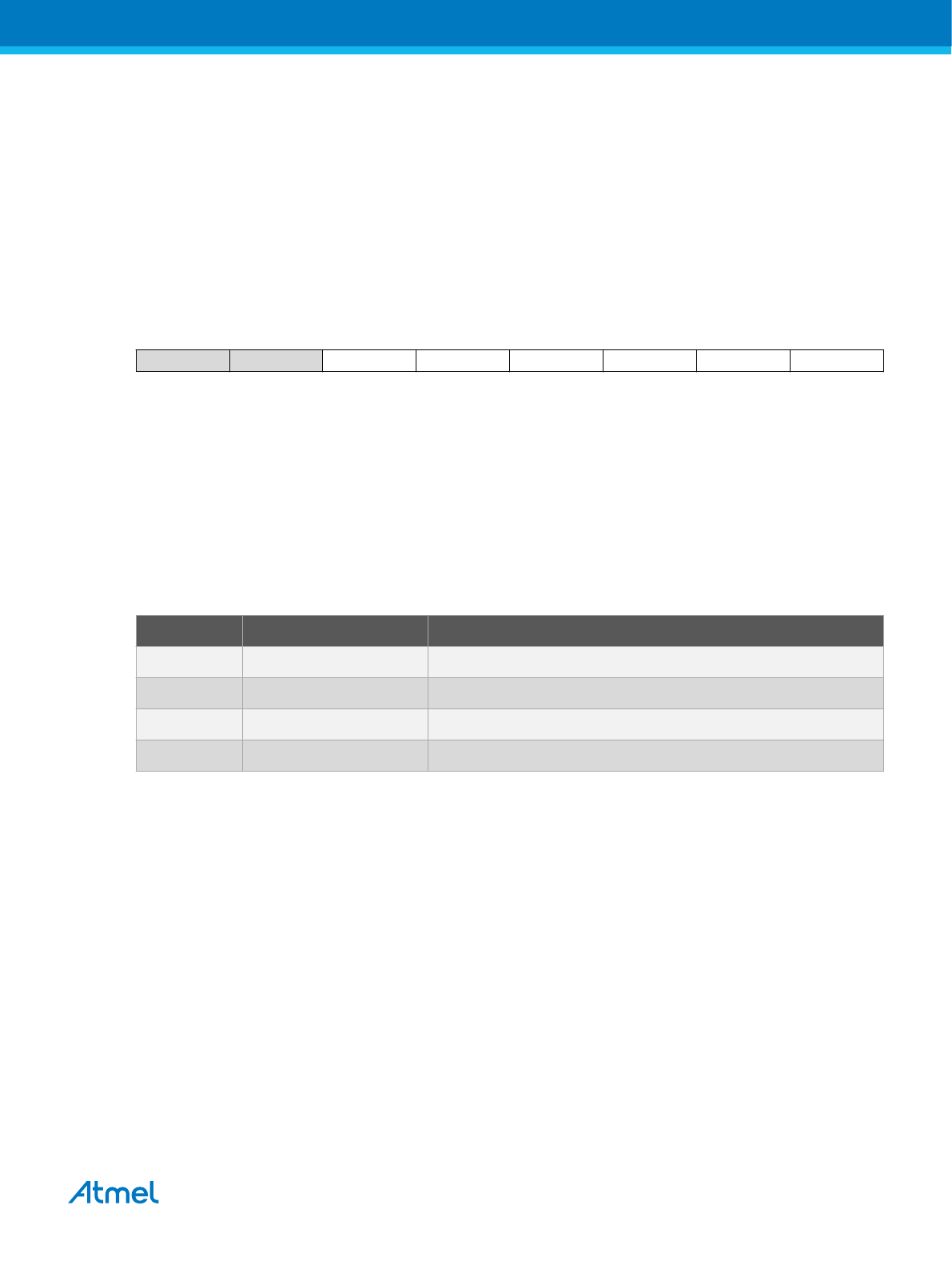
12.6.4. EEPROM Control Register
When addressing I/O Registers as data space using LD and ST instructions, the provided offset must be
used. When using the I/O specific commands IN and OUT, the offset is reduced by 0x20, resulting in an
I/O address offset within 0x00 - 0x3F.
Name: EECR
Offset: 0x3F
Reset: 0x00
Property:
When addressing as I/O Register: address offset is 0x1F
Bit 7 6 5 4 3 2 1 0
EEPM1 EEPM0 EERIE EEMPE EEPE EERE
Access
R/W R/W R/W R/W R/W R/W
Reset x x 0 0 x 0
Bits 5:4 – EEPMn: EEPROM Programming Mode Bits [n = 1:0]
The EEPROM Programming mode bit setting defines which programming action that will be triggered
when writing EEPE. It is possible to program data in one atomic operation (erase the old value and
program the new value) or to split the Erase and Write operations in two different operations. The
Programming times for the different modes are shown in the table below. While EEPE is set, any write to
EEPMn will be ignored. During reset, the EEPMn bits will be reset to 0b00 unless the EEPROM is busy
programming.
Table 12-1. EEPROM Mode Bits
EEPM[1:0] Programming Time Operation
00 3.4ms Erase and Write in one operation (Atomic Operation)
01 1.8ms Erase Only
10 1.8ms Write Only
11 - Reserved for future use
Bit 3 – EERIE: EEPROM Ready Interrupt Enable
Writing EERIE to one enables the EEPROM Ready Interrupt if the I bit in SREG is set. Writing EERIE to
zero disables the interrupt. The EEPROM Ready interrupt generates a constant interrupt when EEPE is
cleared. The interrupt will not be generated during EEPROM write or SPM.
Bit 2 – EEMPE: EEPROM Master Write Enable
The EEMPE bit determines whether writing EEPE to '1' causes the EEPROM to be written.
When EEMPE is '1', setting EEPE within four clock cycles will write data to the EEPROM at the selected
address.
If EEMPE is zero, setting EEPE will have no effect. When EEMPE has been written to '1' by software,
hardware clears the bit to zero after four clock cycles. See the description of the EEPE bit for an
EEPROM write procedure.
Bit 1 – EEPE: EEPROM Write Enable
The EEPROM Write Enable Signal EEPE is the write strobe to the EEPROM. When address and data are
correctly set up, the EEPE bit must be written to '1' to write the value into the EEPROM. The EEMPE bit
Atmel ATmega328/P [DATASHEET]
Atmel-42735B-ATmega328/P_Datasheet_Complete-11/2016
42
Page 43
must be written to '1' before EEPE is written to '1', otherwise no EEPROM write takes place. The following
procedure should be followed when writing the EEPROM (the order of steps 3 and 4 is not essential):
1. Wait until EEPE becomes zero.
2. Wait until SPMEN in SPMCSR becomes zero.
3. Write new EEPROM address to EEAR (optional).
4. Write new EEPROM data to EEDR (optional).
5. Write a '1' to the EEMPE bit while writing a zero to EEPE in EECR.
6. Within four clock cycles after setting EEMPE, write a '1' to EEPE.
The EEPROM can not be programmed during a CPU write to the Flash memory. The software must
check that the Flash programming is completed before initiating a new EEPROM write. Step 2 is only
relevant if the software contains a Boot Loader allowing the CPU to program the Flash. If the Flash is
never being updated by the CPU, step 2 can be omitted.
Caution:
An interrupt between step 5 and step 6 will make the write cycle fail, since the EEPROM Master
Write Enable will time-out. If an interrupt routine accessing the EEPROM is interrupting another
EEPROM access, the EEAR or EEDR Register will be modified, causing the interrupted
EEPROM access to fail. It is recommended to have the Global Interrupt Flag cleared during all
the steps to avoid these problems.
When the write access time has elapsed, the EEPE bit is cleared by hardware. The user
software can poll this bit and wait for a zero before writing the next byte. When EEPE has been
set, the CPU is halted for two cycles before the next instruction is executed.
Bit 0 – EERE: EEPROM Read Enable
The EEPROM Read Enable Signal EERE is the read strobe to the EEPROM. When the correct address
is set up in the EEAR Register, the EERE bit must be written to a '1' to trigger the EEPROM read. The
EEPROM read access takes one instruction, and the requested data is available immediately. When the
EEPROM is read, the CPU is halted for four cycles before the next instruction is executed.
The user should poll the EEPE bit before starting the read operation. If a write operation is in progress, it
is neither possible to read the EEPROM, nor to change the EEAR Register.
The calibrated Oscillator is used to time the EEPROM accesses. See the following table for typical
programming times for EEPROM access from the CPU.
Table 12-2. EEPROM Programming Time
Symbol Number of Calibrated RC Oscillator Cycles Typ. Programming Time
EEPROM write (from CPU) 26,368 3.3ms
The following code examples show one assembly and one C function for writing to the EEPROM. The
examples assume that interrupts are controlled (e.g. by disabling interrupts globally) so that no interrupts
will occur during execution of these functions. The examples also assume that no Flash Boot Loader is
present in the software. If such code is present, the EEPROM write function must also wait for any
ongoing SPM command to finish.
Assembly Code Example
(1)
EEPROM_write:
; Wait for completion of previous write
sbic EECR,EEPE
Atmel ATmega328/P [DATASHEET]
Atmel-42735B-ATmega328/P_Datasheet_Complete-11/2016
43
Page 44

rjmp EEPROM_write
; Set up address (r18:r17) in address register
out EEARH, r18
out EEARL, r17
; Write data (r16) to Data Register
out EEDR,r16
; Write logical one to EEMPE
sbi EECR,EEMPE
; Start eeprom write by setting EEPE
sbi EECR,EEPE
ret
C Code Example
(1)
void EEPROM_write(unsigned int uiAddress, unsigned char ucData)
{
/* Wait for completion of previous write */
while(EECR & (1<<EEPE))
;
/* Set up address and Data Registers */
EEAR = uiAddress;
EEDR = ucData;
/* Write logical one to EEMPE */
EECR |= (1<<EEMPE);
/* Start eeprom write by setting EEPE */
EECR |= (1<<EEPE);
}
Note: (1) Please refer to About Code Examples
The next code examples show assembly and C functions for reading the EEPROM. The examples
assume that interrupts are controlled so that no interrupts will occur during execution of these functions.
Assembly Code Example
(1)
EEPROM_read:
; Wait for completion of previous write
sbic EECR,EEPE
rjmp EEPROM_read
; Set up address (r18:r17) in address register
out EEARH, r18
out EEARL, r17
; Start eeprom read by writing EERE
sbi EECR,EERE
; Read data from Data Register
in r16,EEDR
ret
C Code Example
(1)
unsigned char EEPROM_read(unsigned int uiAddress)
{
/* Wait for completion of previous write */
while(EECR & (1<<EEPE))
;
/* Set up address register */
EEAR = uiAddress;
/* Start eeprom read by writing EERE */
EECR |= (1<<EERE);
/* Return data from Data Register */
return EEDR;
}
Note: (1) Please refer to About Code Examples
Atmel ATmega328/P [DATASHEET]
Atmel-42735B-ATmega328/P_Datasheet_Complete-11/2016
44
Page 45

12.6.5. GPIOR2 – General Purpose I/O Register 2
When addressing I/O Registers as data space using LD and ST instructions, the provided offset must be
used. When using the I/O specific commands IN and OUT, the offset is reduced by 0x20, resulting in an
I/O address offset within 0x00 - 0x3F.
Name: GPIOR2
Offset: 0x4B
Reset: 0x00
Property:
When addressing as I/O Register: address offset is 0x2B
Bit 7 6 5 4 3 2 1 0
GPIOR2[7:0]
Access
R/W R/W R/W R/W R/W R/W R/W R/W
Reset 0 0 0 0 0 0 0 0
Bits 7:0 – GPIOR2[7:0]: General Purpose I/O
Atmel ATmega328/P [DATASHEET]
Atmel-42735B-ATmega328/P_Datasheet_Complete-11/2016
45
Page 46

12.6.6. GPIOR1 – General Purpose I/O Register 1
When addressing I/O Registers as data space using LD and ST instructions, the provided offset must be
used. When using the I/O specific commands IN and OUT, the offset is reduced by 0x20, resulting in an
I/O address offset within 0x00 - 0x3F.
Name: GPIOR1
Offset: 0x4A
Reset: 0x00
Property:
When addressing as I/O Register: address offset is 0x2A
Bit 7 6 5 4 3 2 1 0
GPIOR1[7:0]
Access
R/W R/W R/W R/W R/W R/W R/W R/W
Reset 0 0 0 0 0 0 0 0
Bits 7:0 – GPIOR1[7:0]: General Purpose I/O
Atmel ATmega328/P [DATASHEET]
Atmel-42735B-ATmega328/P_Datasheet_Complete-11/2016
46
Page 47

12.6.7. GPIOR0 – General Purpose I/O Register 0
When addressing I/O Registers as data space using LD and ST instructions, the provided offset must be
used. When using the I/O specific commands IN and OUT, the offset is reduced by 0x20, resulting in an
I/O address offset within 0x00 - 0x3F.
Name: GPIOR0
Offset: 0x3E
Reset: 0x00
Property:
When addressing as I/O Register: address offset is 0x1E
Bit 7 6 5 4 3 2 1 0
GPIOR0[7:0]
Access
R/W R/W R/W R/W R/W R/W R/W R/W
Reset 0 0 0 0 0 0 0 0
Bits 7:0 – GPIOR0[7:0]: General Purpose I/O
Atmel ATmega328/P [DATASHEET]
Atmel-42735B-ATmega328/P_Datasheet_Complete-11/2016
47
Page 48
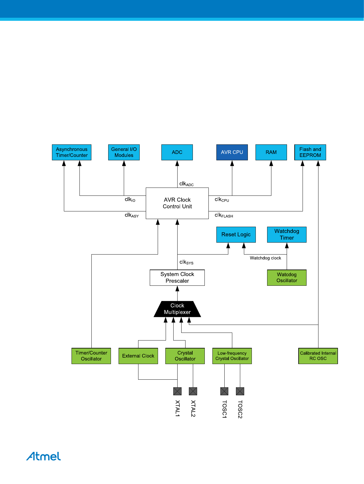
13. System Clock and Clock Options
13.1. Clock Systems and Their Distribution
The following figure illustrates the principal clock systems in the device and their distribution. All the
clocks need not be active at a given time. In order to reduce power consumption, the clocks to modules
not being used can be halted by using different sleep modes. The clock systems are described in the
following sections.
The system clock frequency refers to the frequency generated from the System Clock Prescaler. All clock
outputs from the AVR Clock Control Unit runs in the same frequency.
Figure 13-1. Clock Distribution
Atmel ATmega328/P [DATASHEET]
Atmel-42735B-ATmega328/P_Datasheet_Complete-11/2016
48
Page 49

13.1.1. CPU Clock – clk
CPU
The CPU clock is routed to parts of the system concerned with operation of the AVR core. Examples of
such modules are the General Purpose Register File, the Status Register and the data memory holding
the Stack Pointer. Halting the CPU clock inhibits the core from performing general operations and
calculations.
13.1.2. I/O Clock – clk
I/O
The I/O clock is used by the majority of the I/O modules, like Timer/Counters, SPI, and USART. The I/O
clock is also used by the External Interrupt module, but the start condition detection in the USI module is
carried out asynchronously when clk
I/O
is halted, TWI address recognition in all sleep modes.
Note: If a level triggered interrupt is used for wake-up from Power-down, the required level must be held
long enough for the MCU to complete the wake-up to trigger the level interrupt. If the level disappears
before the end of the Start-up Time, the MCU will still wake up, but no interrupt will be generated. The
start-up time is defined by the SUT and CKSEL Fuses.
13.1.3. Flash Clock – clk
FLASH
The Flash clock controls operation of the Flash interface. The Flash clock is usually active simultaneously
with the CPU clock.
13.1.4. Asynchronous Timer Clock – clk
ASY
The Asynchronous Timer clock allows Asynchronous Timer/Counters to be clocked directly from an
external clock or an external 32kHz clock crystal. The dedicated clock domain allows using this Timer/
Counter as a real-time counter even when the device is in sleep mode.
13.1.5. ADC Clock – clk
ADC
The ADC is provided with a dedicated clock domain. This allows halting the CPU and I/O clocks in order
to reduce noise generated by digital circuitry. This gives more accurate ADC conversion results.
13.2. Clock Sources
The device has the following clock source options, selectable by Flash Fuse bits as shown below. The
clock from the selected source is input to the AVR clock generator, and routed to the appropriate
modules.
Table 13-1. Device Clocking Options Select
Device Clocking Option CKSEL[3:0]
Low Power Crystal Oscillator 1111 - 1000
Full Swing Crystal Oscillator 0111 - 0110
Low Frequency Crystal Oscillator 0101 - 0100
Internal 128kHz RC Oscillator 0011
Calibrated Internal RC Oscillator 0010
External Clock 0000
Reserved 0001
Note: For all fuses, '1' means unprogrammed while '0' means programmed.
Atmel ATmega328/P [DATASHEET]
Atmel-42735B-ATmega328/P_Datasheet_Complete-11/2016
49
Page 50

13.2.1. Default Clock Source
The device is shipped with internal RC oscillator at 8.0MHz and with the fuse CKDIV8 programmed,
resulting in 1.0MHz system clock. The startup time is set to maximum, and the time-out period is enabled:
CKSEL=0010, SUT=10, CKDIV8=0. This default setting ensures that all users can make their desired
clock source setting using any available programming interface.
13.2.2. Clock Startup Sequence
Any clock source needs a sufficient V
CC
to start oscillating and a minimum number of oscillating cycles
before it can be considered stable.
To ensure sufficient V
CC
, the device issues an internal reset with a time-out delay (t
TOUT
) after the device
reset is released by all other reset sources. See the Related Links for a description of the start conditions
for the internal reset. The delay (t
TOUT
) is timed from the Watchdog Oscillator and the number of cycles in
the delay is set by the SUTx and CKSELx fuse bits. The selectable delays are shown in the Table below.
The frequency of the Watchdog Oscillator is voltage dependent.
Table 13-2. Number of Watchdog Oscillator Cycles
Typ. Time-out (V
CC
= 5.0V) Typ. Time-out (V
CC
= 3.0V) Number of Cycles
0ms 0ms 0
4.1ms 4.3ms 512
65ms 69ms 8K (8,192)
Main purpose of the delay is to keep the device in reset until it is supplied with minimum V
CC
. The delay
will not monitor the actual voltage, so it is required to select a delay longer than the V
CC
rise time. If this is
not possible, an internal or external Brown-Out Detection circuit should be used. A BOD circuit will ensure
sufficient V
CC
before it releases the reset, and the time-out delay can be disabled. Disabling the time-out
delay without utilizing a Brown-Out Detection circuit is not recommended.
The oscillator is required to oscillate for a minimum number of cycles before the clock is considered
stable. An internal ripple counter monitors the oscillator output clock, and keeps the internal reset active
for a given number of clock cycles. The reset is then released and the device will start to execute. The
recommended oscillator start-up time is dependent on the clock type, and varies from 6 cycles for an
externally applied clock to 32K cycles for a low frequency crystal.
The start-up sequence for the clock includes both the time-out delay and the start-up time when the
device starts up from reset. When starting up from Power-save or Power-down mode, V
CC
is assumed to
be at a sufficient level and only the start-up time is included.
13.2.3. Low Power Crystal Oscillator
Pins XTAL1 and XTAL2 are input and output, respectively, of an inverting amplifier which can be
configured for use as an On-chip Oscillator, as shown in the Figure below. Either a quartz crystal or a
ceramic resonator may be used.
C1 and C2 should always be equal for both crystals and resonators. The optimal value of the capacitors
depends on the crystal or resonator in use, the amount of stray capacitance, and the electromagnetic
noise of the environment. Some initial guidelines for choosing capacitors for use with crystals are given in
the next Table. For ceramic resonators, the capacitor values given by the manufacturer should be used.
Atmel ATmega328/P [DATASHEET]
Atmel-42735B-ATmega328/P_Datasheet_Complete-11/2016
50
Page 51
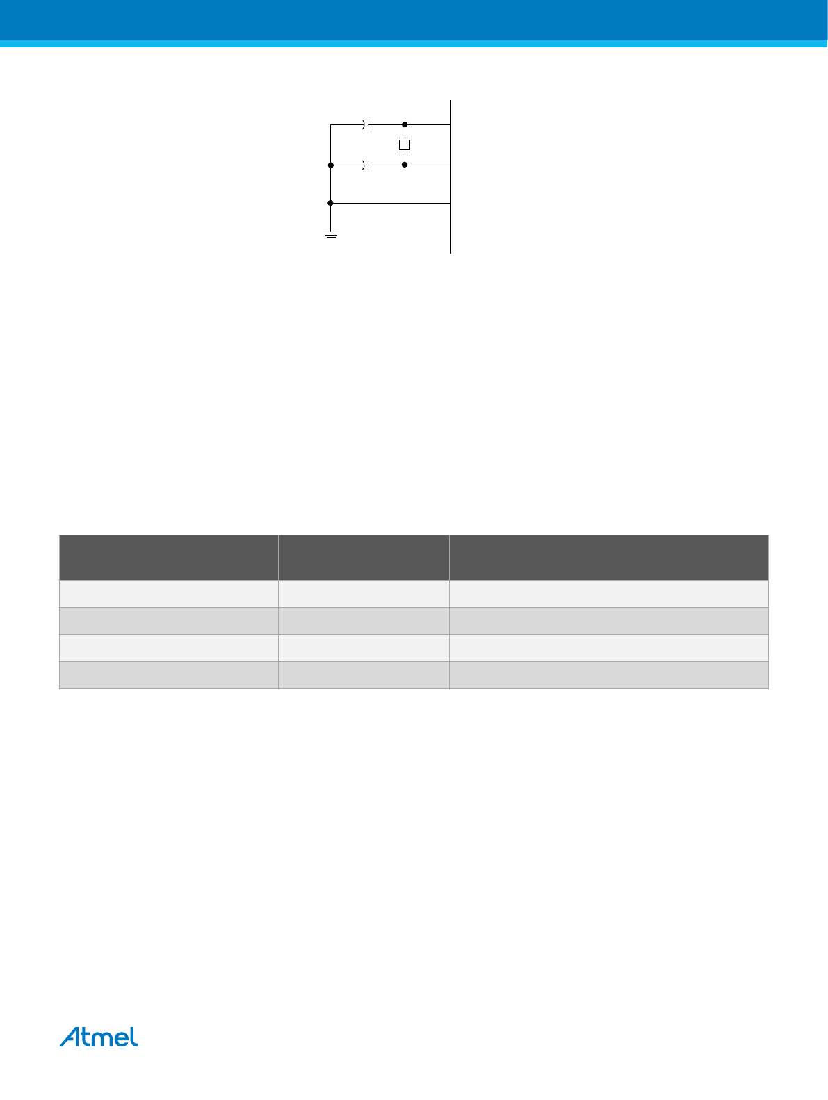
Figure 13-2. Crystal Oscillator Connections
XTAL2
XTAL1
GND
C2
C1
Related Links
Low Power Crystal Oscillator on page 51
Full Swing Crystal Oscillator on page 52
13.3. Low Power Crystal Oscillator
This Crystal Oscillator is a low power oscillator, with reduced voltage swing on the XTAL2 output. It gives
the lowest power consumption, but is not capable of driving other clock inputs, and may be more
susceptible to noise in noisy environments. In these cases, refer to Full Swing Crystal Oscillator.
The crystal should be connected as described in Clock Source Connections.
The Low Power Oscillator can operate in three different modes, each optimized for a specific frequency
range. The operating mode is selected by the fuses CKSEL[3:1], as shown in the following table:
Table 13-3. Low Power Crystal Oscillator Operating Modes
(1)
Frequency Range
[MHz]
CKSEL[3:1]
(2)
Range for
Capacitors C1 and C2 [pF]
0.4 - 0.9 100
(3)
–
0.9 - 3.0 101 12 - 22
3.0 - 8.0 110 12 - 22
8.0 - 16.0 111 12 - 22
Note:
1. If the crystal frequency exceeds the specification of the device (depends on V
CC
), the CKDIV8 Fuse
can be programmed in order to divide the internal frequency by 8. It must be ensured that the
resulting divided clock meets the frequency specification of the device.
2. This is the recommended CKSEL settings for the difference frequency ranges.
3. This option should not be used with crystals, only with ceramic resonators.
The CKSEL0 Fuse together with the SUT[1:0] Fuses select the start-up times, as shown in the following
table:
Atmel ATmega328/P [DATASHEET]
Atmel-42735B-ATmega328/P_Datasheet_Complete-11/2016
51
Page 52

Table 13-4. Start-up Times for the Low Power Crystal Oscillator Clock Selection
Oscillator Source / Power
Conditions
Start-up Time from
Power-down and
Power-save
Additional Delay from
Reset
(V
CC
= 5.0V)
CKSEL0 SUT[1:0]
Ceramic resonator, fast rising power 258 CK 14CK + 4.1ms
(1)
0 00
Ceramic resonator, slowly rising
power
258 CK 14CK + 65ms
(1)
0 01
Ceramic resonator, BOD enabled 1K CK 14CK
(2)
0 10
Ceramic resonator, fast rising power 1K CK 14CK + 4.1ms
(2)
0 11
Ceramic resonator, slowly rising
power
1K CK 14CK + 65ms
(2)
1 00
Crystal Oscillator, BOD enabled 16K CK 14CK 1 01
Crystal Oscillator, fast rising power 16K CK 14CK + 4.1ms 1 10
Crystal Oscillator, slowly rising power 16K CK 14CK + 65ms 1 11
Note:
1. These options should only be used when not operating close to the maximum frequency of the
device, and only if frequency stability at start-up is not important for the application. These options
are not suitable for crystals.
2. These options are intended for use with ceramic resonators and will ensure frequency stability at
start-up. They can also be used with crystals when not operating close to the maximum frequency
of the device, and if frequency stability at start-up is not important for the application.
Related Links
Low Power Crystal Oscillator on page 50
13.4. Full Swing Crystal Oscillator
This Crystal Oscillator is a full swing oscillator, with rail-to-rail swing on the XTAL2 output. This is useful
for driving other clock inputs and in noisy environments. The current consumption is higher than for the
Low Power Crystal Oscillator. Note that the Full Swing Crystal Oscillator will only operate for
V
CC
=2.7-5.5V.
Some initial guidelines for choosing capacitors for use with crystals are given in Table 13-6. The crystal
should be connected as described in Clock Source Connections”.
The operating mode is selected based on the fuses CKSEL[3:1] as shown in the table:
Table 13-5. Full Swing Crystal Oscillator operating modes
Frequency Range
(1)
[MHz] CKSEL[3:1] Recommended Range for Capacitors C1 and C2 [pF]
0.4 - 20 011 12 - 22
Note:
1. If the crystal frequency exceeds the specification of the device (depends on V
CC
), the CKDIV8 Fuse
can be programmed in order to divide the internal frequency by 8. It must be ensured that the
resulting divided clock meets the frequency specification of the device.
Atmel ATmega328/P [DATASHEET]
Atmel-42735B-ATmega328/P_Datasheet_Complete-11/2016
52
Page 53
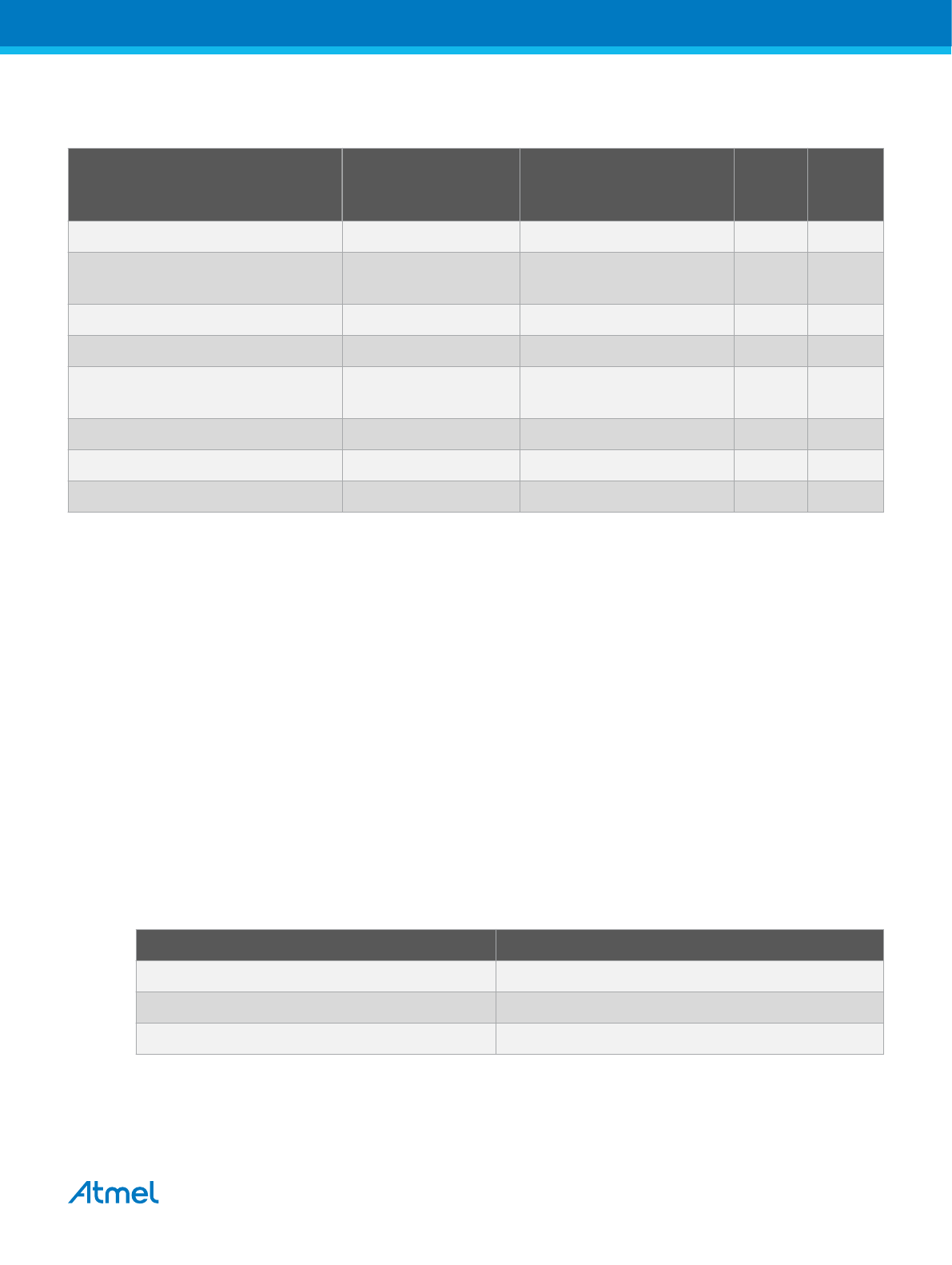
For the Crystall Oscillator connections refer to Low Power Crystal Oscillator.
Table 13-6. Start-Up Times for the Full Swing Crystal Oscillator Clock Selection
Oscillator Source / Power
Conditions
Start-Up Time from
Power-down and
Power-save
Additional Delay from
Reset
(V
CC
= 5.0V)
CKSEL0 SUT[1:0]
Ceramic resonator, fast rising power 258 CK 14CK + 4.1ms
(1)
0 00
Ceramic resonator, slowly rising
power
258 CK 14CK + 65ms
(1)
0 01
Ceramic resonator, BOD enabled 1K CK 14CK
(2)
0 10
Ceramic resonator, fast rising power 1K CK 14CK + 4.1ms
(2)
0 11
Ceramic resonator, slowly rising
power
1K CK 14CK + 65ms
(2)
1 00
Crystal Oscillator, BOD enabled 16K CK 14CK 1 01
Crystal Oscillator, fast rising power 16K CK 14CK + 4.1ms 1 10
Crystal Oscillator, slowly rising power 16K CK 14CK + 65ms 1 11
Note:
1. These options should only be used when not operating close to the maximum frequency of the
device, and only if frequency stability at start-up is not important for the application. These options
are not suitable for crystals.
2. These options are intended for use with ceramic resonators and will ensure frequency stability at
start-up. They can also be used with crystals when not operating close to the maximum frequency
of the device, and if frequency stability at start-up is not important for the application.
Related Links
Low Power Crystal Oscillator on page 50
13.5. Low Frequency Crystal Oscillator
The Low-frequency Crystal Oscillator is optimized for use with a 32.768kHz watch crystal. When selecting
crystals, load capacitance and crystal’s Equivalent Series Resistance (ESR) must be taken into
consideration. Both values are specified by the crystal vendor. The oscillator is optimized for very low
power consumption, and thus when selecting crystals, consider the Maximum ESR Recommendations:
Table 13-7. Maximum ESR Recommendation for 32.768kHz Crystal
Crystal CL [pF] Max. ESR [kΩ]
(1)
6.5 75
9.0 65
12.5 30
Note:
1. Maximum ESR is typical value based on characterization.
The Low-frequency Crystal Oscillator provides an internal load capacitance at each TOSC pin:
Atmel ATmega328/P [DATASHEET]
Atmel-42735B-ATmega328/P_Datasheet_Complete-11/2016
53
Page 54

Table 13-8. Capacitance for Low-Frequency Oscillator
32kHz Osc. Type Cap. (XTAL1/TOSC1) Cap. (XTAL2/TSOC2)
System Osc. 18pF 8pF
Timer Osc. 6pF 6pF
The capacitance (Ce+Ci) needed at each TOSC pin can be calculated by using:
= 2C
where:
• Ce - is optional external capacitors as described in Figure 13-2.
• Ci - is the pin capacitance in the above table.
• CL - is the load capacitance for a 32.768kHz crystal specified by the crystal vendor.
• C
S
- is the total stray capacitance for one TOSC pin.
Crystals specifying a load capacitance (CL) higher than 6pF require external capacitors applied as
described in Low Power Crystal Oscillator.
The Low-frequency Crystal Oscillator must be selected by setting the CKSEL Fuses to 0110 or 0111.
Table 13-9. Start-up Times for the Low-frequency Crystal Oscillator Clock Selection
CKSEL[3:0] Start-up Time from Power-down and Power-save Recommended Usage
0100
(1)
1K CK
0101 32K CK Stable frequency at start-up
Note:
1. This option should only be used if frequency stability at start-up is not important for the application
Start-up times are determined by the SUT Fuses as shown in the following table.
Table 13-10. Start-up Times for the Low Frequency Crystal Oscillator Clock Selection
SUT[1:0] Additional Delay from Reset (V
CC
= 5.0V) Power Conditions
00 14CK BOD enabled
01 14CK + 4.1 ms Fast rising power
10 14CK + 65 ms Slowly rising power
11 Reserved
Related Links
Timer/Counter Oscillator on page 57
13.6. Calibrated Internal RC Oscillator
By default, the Internal RC Oscillator provides an 8.0MHz clock. Though voltage and temperature
dependent, this clock can be very accurately calibrated by the user. The device is shipped with the
CKDIV8 Fuse programmed.
This clock may be selected as the system clock by programming the CKSEL Fuses as shown in the
following Table. If selected, it will operate with no external components. During reset, hardware loads the
Atmel ATmega328/P [DATASHEET]
Atmel-42735B-ATmega328/P_Datasheet_Complete-11/2016
54
Page 55
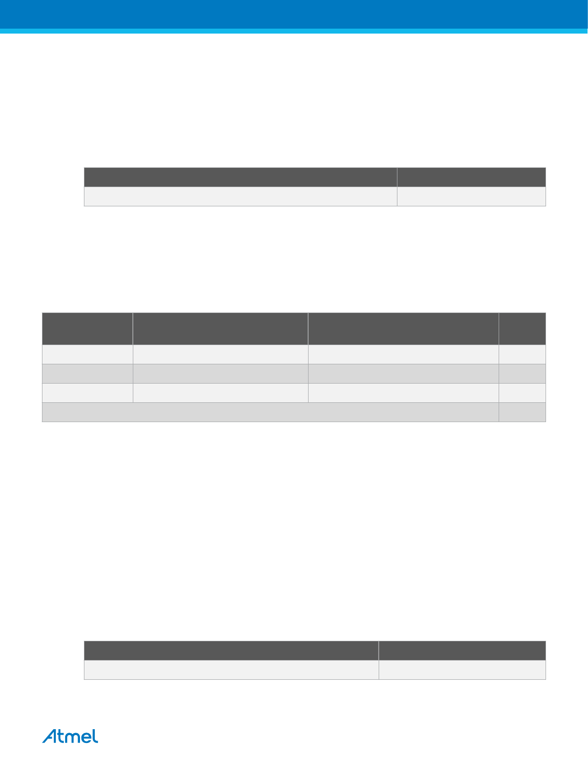
pre-programmed calibration value into the OSCCAL Register and thereby automatically calibrates the RC
Oscillator.
By changing the OSCCAL register from SW, it is possible to get a higher calibration accuracy than by
using the factory calibration.
When this Oscillator is used as the chip clock, the Watchdog Oscillator will still be used for the Watchdog
Timer and for the Reset Time-Out. For more information on the pre-programmed calibration value.
Table 13-11. Internal Calibrated RC Oscillator Operating Modes
Frequency Range
(1)
[MHz] CKSEL[3:0]
7.3 - 8.1 0010
(2)
Note:
1. If 8MHz frequency exceeds the specification of the device (depends on V
CC
), the CKDIV8 Fuse can
be programmed in order to divide the internal frequency by 8.
2. The device is shipped with this option selected.
When this Oscillator is selected, start-up times are determined by the SUT Fuses:
Table 13-12. Start-Up Times for the Internal Calibrated RC Oscillator Clock Selection - SUT
Power Conditions Start-Up Time from Power-down
and Power-Save
Additional Delay from Reset (V
CC
=
5.0V)
SUT[1:0]
BOD enabled 6 CK 14CK 00
Fast rising power 6 CK 14CK + 4.1ms 01
Slowly rising power 6 CK 14CK + 65ms 10
(1)
Reserved 11
Note:
1. The device is shipped with this option selected.
Related Links
Clock Characteristics on page 369
System Clock Prescaler on page 57
Calibration Byte on page 351
OSCCAL on page 59
13.7. 128kHz Internal Oscillator
The 128kHz internal Oscillator is a low power Oscillator providing a clock of 128kHz. The frequency is
nominal at 3V and 25°C. This clock may be select as the system clock by programming the CKSEL Fuses
to '0011':
Table 13-13. 128kHz Internal Oscillator Operating Modes
Nominal Frequency
(1)
CKSEL[3:0]
128kHz 0011
Note:
Atmel ATmega328/P [DATASHEET]
Atmel-42735B-ATmega328/P_Datasheet_Complete-11/2016
55
Page 56
1. The 128kHz oscillator is a very low power clock source, and is not designed for high accuracy.
When this clock source is selected, start-up times are determined by the SUT Fuses:
Table 13-14. Start-Up Times for the 128kHz Internal Oscillator
Power Conditions Start-Up Time from Power-down and Power-
save
Additional Delay from Reset SUT[1:0]
BOD enabled 6 CK 14CK 00
Fast rising power 6 CK 14CK + 4ms 01
Slowly rising power 6 CK 14CK + 64ms 10
Reserved 11
13.8. External Clock
To drive the device from an external clock source, EXTCLK should be driven as shown in the Figure
below. To run the device on an external clock, the CKSEL Fuses must be programmed to '0000':
Table 13-15. External Clock Frequency
Frequency
(1)
CKSEL[3:0]
0 - 20MHz 0000
Note:
1. If the cryatal frequency exceeds the specification of the device (depends on VCC), the CKDIV8
Fuse can be programmed in order to divide the internal frequency by 8. It must be ensured that the
resulting divided clock meets the frequency specification of the device.
Figure 13-3. External Clock Drive Configuration
EXTERNAL
CLOCK
SIGNAL
EXTCLK
GND
When this clock source is selected, start-up times are determined by the SUT Fuses:
Table 13-16. Start-Up Times for the External Clock Selection - SUT
Power Conditions Start-Up Time from Power-down
and Power-save
Additional Delay from Reset (V
CC
=
5.0V)
SUT[1:0]
BOD enabled 6 CK 14CK 00
Fast rising power 6 CK 14CK + 4ms 01
Atmel ATmega328/P [DATASHEET]
Atmel-42735B-ATmega328/P_Datasheet_Complete-11/2016
56
Page 57

Power Conditions Start-Up Time from Power-down
and Power-save
Additional Delay from Reset (V
CC
=
5.0V)
SUT[1:0]
Slowly rising power 6 CK 14CK + 65ms 10
Reserved 11
When applying an external clock, it is required to avoid sudden changes in the applied clock frequency to
ensure stable operation of the MCU. A variation in frequency of more than 2% from one clock cycle to the
next can lead to unpredictable behavior. If changes of more than 2% is required, ensure that the MCU is
kept in Reset during the changes.
The System Clock Prescaler can be used to implement run-time changes of the internal clock frequency
while still ensuring stable operation.
Related Links
System Clock Prescaler on page 57
13.9. Timer/Counter Oscillator
The device uses the same crystal oscillator for Low-frequency Oscillator and Timer/Counter Oscillator.
See Low Frequency Crystal Oscillator for details on the oscillator and crystal requirements.
On this device, the Timer/Counter Oscillator Pins (TOSC1 and TOSC2) are shared with XTAL1 and
XTAL2. When using the Timer/Counter Oscillator, the system clock needs to be four times the oscillator
frequency. Due to this and the pin sharing, the Timer/Counter Oscillator can only be used when the
Calibrated Internal RC Oscillator is selected as system clock source.
Applying an external clock source to TOSC1 can be done if the Enable External Clock Input bit in the
Asynchronous Status Register (ASSR.EXCLK) is written to '1'. See the description of the Asynchronous
Operation of Timer/Counter2 for further description on selecting external clock as input instead of a
32.768kHz watch crystal.
Related Links
OCR2B on page 210
ASSR on page 213
Low Frequency Crystal Oscillator on page 53
13.10. Clock Output Buffer
The device can output the system clock on the CLKO pin. To enable the output, the CKOUT Fuse has to
be programmed. This mode is suitable when the chip clock is used to drive other circuits on the system.
The clock also will be output during reset, and the normal operation of I/O pin will be overridden when the
fuse is programmed. Any clock source, including the internal RC Oscillator, can be selected when the
clock is output on CLKO. If the System Clock Prescaler is used, it is the divided system clock that is
output.
13.11. System Clock Prescaler
The device has a system clock prescaler, and the system clock can be divided by configuring the Clock
Prescale Register (CLKPR). This feature can be used to decrease the system clock frequency and the
power consumption when the requirement for processing power is low. This can be used with all clock
Atmel ATmega328/P [DATASHEET]
Atmel-42735B-ATmega328/P_Datasheet_Complete-11/2016
57
Page 58

source options, and it will affect the clock frequency of the CPU and all synchronous peripherals. clk
I/O
,
clk
ADC
, clk
CPU
, and clk
FLASH
are divided by a factor as shown in the CLKPR description.
When switching between prescaler settings, the System Clock Prescaler ensures that no glitches occurs
in the clock system. It also ensures that no intermediate frequency is higher than neither the clock
frequency corresponding to the previous setting, nor the clock frequency corresponding to the new
setting. The ripple counter that implements the prescaler runs at the frequency of the undivided clock,
which may be faster than the CPU's clock frequency. Hence, it is not possible to determine the state of
the prescaler - even if it were readable, the exact time it takes to switch from one clock division to the
other cannot be exactly predicted. From the time the Clock Prescaler Selection bits (CLKPS[3:0]) values
are written, it takes between T1 + T2 and T1 + 2 * T2 before the new clock frequency is active. In this
interval, two active clock edges are produced. Here, T1 is the previous clock period, and T2 is the period
corresponding to the new prescaler setting.
To avoid unintentional changes of clock frequency, a special write procedure must be followed to change
the CLKPS bits:
1. Write the Clock Prescaler Change Enable (CLKPCE) bit to '1' and all other bits in CLKPR to zero:
CLKPR=0x80.
2. Within four cycles, write the desired value to CLKPS[3:0] while writing a zero to CLKPCE:
CLKPR=0x0N
Interrupts must be disabled when changing prescaler setting to make sure the write procedure is not
interrupted.
Related Links
Calibrated Internal RC Oscillator on page 54
External Clock on page 56
CLKPR on page 60
13.12. Register Description
Atmel ATmega328/P [DATASHEET]
Atmel-42735B-ATmega328/P_Datasheet_Complete-11/2016
58
Page 59

13.12.1. Oscillator Calibration Register
Name: OSCCAL
Offset: 0x66
Reset: Device Specific Calibration Value
Property:
-
Bit 7 6 5 4 3 2 1 0
CAL7 CAL6 CAL5 CAL4 CAL3 CAL2 CAL1 CAL0
Access
R/W R/W R/W R/W R/W R/W R/W R/W
Reset x x x x x x x x
Bits 7:0 – CALn: Oscillator Calibration Value [n = 7:0]
The Oscillator Calibration Register is used to trim the Calibrated Internal RC Oscillator to remove process
variations from the oscillator frequency. A pre-programmed calibration value is automatically written to
this register during chip reset, giving the Factory calibrated frequency as specified in the Clock
Characteristics section of Electrical Characteristics chapter.. The application software can write this
register to change the oscillator frequency. The oscillator can be calibrated to frequencies as specified in
the Clock Characteristics section of Electrical Characteristics chapter.. Calibration outside that range is
not guaranteed.
Note that this oscillator is used to time EEPROM and Flash write accesses, and these write times will be
affected accordingly. If the EEPROM or Flash are written, do not calibrate to more than 8.8MHz.
Otherwise, the EEPROM or Flash write may fail.
The CAL7 bit determines the range of operation for the oscillator. Setting this bit to 0 gives the lowest
frequency range, setting this bit to 1 gives the highest frequency range. The two frequency ranges are
overlapping, in other words a setting of OSCCAL=0x7F gives a higher frequency than OSCCAL=0x80.
The CAL[6:0] bits are used to tune the frequency within the selected range. A setting of 0x00 gives the
lowest frequency in that range, and a setting of 0x7F gives the highest frequency in the range.
Atmel ATmega328/P [DATASHEET]
Atmel-42735B-ATmega328/P_Datasheet_Complete-11/2016
59
Page 60
13.12.2. Clock Prescaler Register
Name: CLKPR
Offset: 0x61
Reset: Refer to the bit description
Property:
-
Bit 7 6 5 4 3 2 1 0
CLKPCE CLKPS3 CLKPS2 CLKPS1 CLKPS0
Access
R/W R/W R/W R/W R/W
Reset 0 x x x x
Bit 7 – CLKPCE: Clock Prescaler Change Enable
The CLKPCE bit must be written to logic one to enable change of the CLKPS bits. The CLKPCE bit is
only updated when the other bits in CLKPR are simultaneously written to zero. CLKPCE is cleared by
hardware four cycles after it is written or when CLKPS bits are written. Rewriting the CLKPCE bit within
this time-out period does neither extend the time-out period, nor clear the CLKPCE bit.
Bits 3:0 – CLKPSn: Clock Prescaler Select n [n = 3:0]
These bits define the division factor between the selected clock source and the internal system clock.
These bits can be written run-time to vary the clock frequency to suit the application requirements. As the
divider divides the master clock input to the MCU, the speed of all synchronous peripherals is reduced
when a division factor is used. The division factors are given in the table below.
The CKDIV8 Fuse determines the initial value of the CLKPS bits. If CKDIV8 is unprogrammed, the
CLKPS bits will be reset to “0000”. If CKDIV8 is programmed, CLKPS bits are reset to “0011”, giving a
division factor of 8 at start up. This feature should be used if the selected clock source has a higher
frequency than the maximum frequency of the device at the present operating conditions. Note that any
value can be written to the CLKPS bits regardless of the CKDIV8 Fuse setting. The Application software
must ensure that a sufficient division factor is chosen if the selected clock source has a higher frequency
than the maximum frequency of the device at the present operating conditions. The device is shipped with
the CKDIV8 Fuse programmed.
Table 13-17. Clock Prescaler Select
CLKPS[3:0] Clock Division Factor
0000 1
0001 2
0010 4
0011 8
0100 16
0101 32
0110 64
0111 128
1000 256
1001 Reserved
Atmel ATmega328/P [DATASHEET]
Atmel-42735B-ATmega328/P_Datasheet_Complete-11/2016
60
Page 61

CLKPS[3:0] Clock Division Factor
1010 Reserved
1011 Reserved
1100 Reserved
1101 Reserved
1110 Reserved
1111 Reserved
Atmel ATmega328/P [DATASHEET]
Atmel-42735B-ATmega328/P_Datasheet_Complete-11/2016
61
Page 62
14. PM - Power Management and Sleep Modes
14.1. Overview
Sleep modes enable the application to shut down unused modules in the MCU, thereby saving power.
The device provides various sleep modes allowing the user to tailor the power consumption to the
application requirements.
When enabled, the Brown-out Detector (BOD) actively monitors the power supply voltage during the
sleep periods. To further save power, it is possible to disable the BOD in some sleep modes. See also
BOD Disable.
Note: BOD disable is only available for ATmega328P.
14.2. Sleep Modes
The following Table shows the different sleep modes, BOD disable ability and their wake-up sources.
Table 14-1. Active Clock Domains and Wake-up Sources in the Different Sleep Modes.
Active Clock Domains Oscillators Wake-up Sources Software
BOD Disable
Sleep Mode clk
CPU
clk
FLASH
clk
IO
clk
ADC
clk
ASY
Main Clock
Source Enabled
Timer Oscillator
Enabled
INT and PCINT TWI Address
Match
Timer2 SPM/EEPROM
Ready
ADC WDT Other I/O
Idle Yes Yes Yes Yes Yes
(2)
Yes Yes Yes Yes Yes Yes Yes
ADC Noise
Reduction
Yes Yes Yes Yes
(2)
Yes
(3)
Yes Yes
(2)
Yes Yes Yes
Power-down Yes
(3)
Yes Yes Yes
Power-save Yes Yes
(2)
Yes
(3)
Yes Yes Yes Yes
Standby
(1)
Yes Yes
(3)
Yes Yes Yes
Extended Standby Yes
(2)
Yes Yes
(2)
Yes
(3)
Yes Yes Yes Yes
Note:
1. Only recommended with external crystal or resonator selected as clock source.
2. If Timer/Counter2 is running in asynchronous mode.
3. For INT1 and INT0, only level interrupt.
To enter any of the six sleep modes, the Sleep Enable bit in the Sleep Mode Control Register (SMCR.SE)
must be written to '1' and a SLEEP instruction must be executed. Sleep Mode Select bits
(SMCR.SM[2:0]) select which sleep mode (Idle, ADC Noise Reduction, Power-down, Power-save,
Standby, or Extended Standby) will be activated by the SLEEP instruction.
Note: The block diagram in the section System Clock and Clock Options provides an overview over the
different clock systems in the device, and their distribution. This figure is helpful in selecting an
appropriate sleep mode.
If an enabled interrupt occurs while the MCU is in a sleep mode, the MCU wakes up. The MCU is then
halted for four cycles in addition to the start-up time, executes the interrupt routine, and resumes
execution from the instruction following SLEEP. The contents of the Register File and SRAM are
unaltered when the device wakes up from sleep. If a reset occurs during sleep mode, the MCU wakes up
and executes from the Reset Vector.
Related Links
System Clock and Clock Options on page 48
Atmel ATmega328/P [DATASHEET]
Atmel-42735B-ATmega328/P_Datasheet_Complete-11/2016
62
Page 63

14.3. BOD Disable
When the Brown-out Detector (BOD) is enabled by BODLEVEL fuses (see also section Fuse Bits), the
BOD is actively monitoring the power supply voltage during a sleep period. To save power, it is possible to
disable the BOD by software for some of the sleep modes. The sleep mode power consumption will then
be at the same level as when BOD is globally disabled by fuses. If BOD is disabled in software, the BOD
function is turned off immediately after entering the sleep mode. Upon wake-up from sleep, BOD is
automatically enabled again. This ensures safe operation in case the V
CC
level has dropped during the
sleep period.
When the BOD has been disabled, the wake-up time from sleep mode will be approximately 60μs to
ensure that the BOD is working correctly before the MCU continues executing code.
BOD disable is controlled by the BOD Sleep bit in the MCU Control Register (MCUCR.BODS). Writing
this bit to '1' turns off the BOD in relevant sleep modes, while a zero in this bit keeps BOD active. The
default setting, BODS=0, keeps BOD active.
Note: Writing to the BODS bit is controlled by a timed sequence and an enable bit.
Note: BOD disable is only available for ATmega328P.
Related Links
MCUCR on page 69
14.4. Idle Mode
When the SM[2:0] bits are written to '000', the SLEEP instruction makes the MCU enter Idle mode,
stopping the CPU but allowing the SPI, USART, Analog Comparator, 2-wire Serial Interface, Timer/
Counters, Watchdog, and the interrupt system to continue operating. This sleep mode basically halts
clk
CPU
and clk
FLASH
, while allowing the other clocks to run.
Idle mode enables the MCU to wake up from external triggered interrupts as well as internal ones like the
Timer Overflow and USART Transmit Complete interrupts. If wake-up from the Analog Comparator
interrupt is not required, the Analog Comparator can be powered down by setting the ACD bit in the
Analog Comparator Control and Status Register – ACSR. This will reduce power consumption in Idle
mode.
14.5. ADC Noise Reduction Mode
When the SM[2:0] bits are written to '001', the SLEEP instruction makes the MCU enter ADC Noise
Reduction mode, stopping the CPU but allowing the ADC, the external interrupts, the 2-wire Serial
Interface address watch, Timer/Counter2
(1)
, and the Watchdog to continue operating (if enabled). This
sleep mode basically halts clk
I/O
, clk
CPU
, and clk
FLASH
, while allowing the other clocks to run.
This improves the noise environment for the ADC, enabling higher resolution measurements. If the ADC
is enabled, a conversion starts automatically when this mode is entered. Apart from the ADC Conversion
Complete interrupt, only these events can wake up the MCU from ADC Noise Reduction mode:
• External Reset
• Watchdog System Reset
• Watchdog Interrupt
• Brown-out Reset
• 2-wire Serial Interface address match
Atmel ATmega328/P [DATASHEET]
Atmel-42735B-ATmega328/P_Datasheet_Complete-11/2016
63
Page 64

• Timer/Counter2 interrupt
• SPM/EEPROM ready interrupt
• External level interrupt on INT
• Pin change interrupt
Note: 1. Timer/Counter2 will only keep running in asynchronous mode.
Related Links
8-bit Timer/Counter2 with PWM and Asynchronous Operation on page 189
14.6. Power-Down Mode
When the SM[2:0] bits are written to '010', the SLEEP instruction makes the MCU enter Power-Down
mode. In this mode, the external Oscillator is stopped, while the external interrupts, the 2-wire Serial
Interface address watch, and the Watchdog continue operating (if enabled).
Only one of these events can wake up the MCU:
• External Reset
• Watchdog System Reset
• Watchdog Interrupt
• Brown-out Reset
• 2-wire Serial Interface address match
• External level interrupt on INT
• Pin change interrupt
This sleep mode basically halts all generated clocks, allowing operation of asynchronous modules only.
Note: If a level triggered interrupt is used for wake-up from Power-Down, the required level must be held
long enough for the MCU to complete the wake-up to trigger the level interrupt. If the level disappears
before the end of the Start-up Time, the MCU will still wake up, but no interrupt will be generated. The
start-up time is defined by the SUT and CKSEL Fuses.
When waking up from Power-Down mode, there is a delay from the wake-up condition occurs until the
wake-up becomes effective. This allows the clock to restart and become stable after having been
stopped. The wake-up period is defined by the same CKSEL Fuses that define the Reset Time-out
period.
Related Links
System Clock and Clock Options on page 48
14.7. Power-save Mode
When the SM[2:0] bits are written to 011, the SLEEP instruction makes the MCU enter Power-save mode.
This mode is identical to Power-down, with one exception:
If Timer/Counter2 is enabled, it will keep running during sleep. The device can wake up from either Timer
Overflow or Output Compare event from Timer/Counter2 if the corresponding Timer/Counter2 interrupt
enable bits are set in TIMSK2, and the Global Interrupt Enable bit in SREG is set.
If Timer/Counter2 is not running, Power-down mode is recommended instead of Power-save mode.
The Timer/Counter2 can be clocked both synchronously and asynchronously in Power-save mode. If
Timer/Counter2 is not using the asynchronous clock, the Timer/Counter Oscillator is stopped during
Atmel ATmega328/P [DATASHEET]
Atmel-42735B-ATmega328/P_Datasheet_Complete-11/2016
64
Page 65

sleep. If Timer/Counter2 is not using the synchronous clock, the clock source is stopped during sleep.
Even if the synchronous clock is running in Power-save, this clock is only available for Timer/Counter2.
14.8. Standby Mode
When the SM[2:0] bits are written to '110' and an external crystal/resonator clock option is selected, the
SLEEP instruction makes the MCU enter Standby mode. This mode is identical to Power-Down with the
exception that the Oscillator is kept running. From Standby mode, the device wakes up in six clock
cycles.
14.9. Extended Standby Mode
When the SM[2:0] bits are written to '111' and an external crystal/resonator clock option is selected, the
SLEEP instruction makes the MCU enter Extended Standby mode. This mode is identical to Power-Save
mode with the exception that the Oscillator is kept running. From Extended Standby mode, the device
wakes up in six clock cycles.
14.10. Power Reduction Register
The Power Reduction Register (PRR) provides a method to stop the clock to individual peripherals to
reduce power consumption. The current state of the peripheral is frozen and the I/O registers can not be
read or written. Resources used by the peripheral when stopping the clock will remain occupied, hence
the peripheral should in most cases be disabled before stopping the clock. Waking up a module, which is
done by clearing the corresponding bit in the PRR, puts the module in the same state as before
shutdown.
Module shutdown can be used in Idle mode and Active mode to significantly reduce the overall power
consumption. In all other sleep modes, the clock is already stopped.
14.11. Minimizing Power Consumption
There are several possibilities to consider when trying to minimize the power consumption in an AVR
controlled system. In general, sleep modes should be used as much as possible, and the sleep mode
should be selected so that as few as possible of the device’s functions are operating. All functions not
needed should be disabled. In particular, the following modules may need special consideration when
trying to achieve the lowest possible power consumption.
14.11.1. Analog to Digital Converter
If enabled, the ADC will be enabled in all sleep modes. To save power, the ADC should be disabled
before entering any sleep mode. When the ADC is turned off and on again, the next conversion will be an
extended conversion.
Related Links
Analog-to-Digital Converter on page 305
14.11.2. Analog Comparator
When entering Idle mode, the Analog Comparator should be disabled if not used. When entering ADC
Noise Reduction mode, the Analog Comparator should be disabled. In other sleep modes, the Analog
Comparator is automatically disabled. However, if the Analog Comparator is set up to use the Internal
Voltage Reference as input, the Analog Comparator should be disabled in all sleep modes. Otherwise,
the Internal Voltage Reference will be enabled, independent of sleep mode.
Atmel ATmega328/P [DATASHEET]
Atmel-42735B-ATmega328/P_Datasheet_Complete-11/2016
65
Page 66

Related Links
Analog Comparator on page 299
14.11.3. Brown-Out Detector
If the Brown-Out Detector (BOD) is not needed by the application, this module should be turned off. If the
BOD is enabled by the BODLEVEL Fuses, it will be enabled in all sleep modes, and hence, always
consume power. In the deeper sleep modes, this will contribute significantly to the total current
consumption.
Related Links
System Control and Reset on page 72
14.11.4. Internal Voltage Reference
The Internal Voltage Reference will be enabled when needed by the Brown-Out Detection, the Analog
Comparator or the Analog-to-Digital Converter. If these modules are disabled as described in the sections
above, the internal voltage reference will be disabled and it will not be consuming power. When turned on
again, the user must allow the reference to start up before the output is used. If the reference is kept on in
sleep mode, the output can be used immediately.
Related Links
System Control and Reset on page 72
14.11.5. Watchdog Timer
If the Watchdog Timer is not needed in the application, the module should be turned off. If the Watchdog
Timer is enabled, it will be enabled in all sleep modes and hence always consume power. In the deeper
sleep modes, this will contribute significantly to the total current consumption.
Related Links
System Control and Reset on page 72
14.11.6. Port Pins
When entering a sleep mode, all port pins should be configured to use minimum power. The most
important is then to ensure that no pins drive resistive loads. In sleep modes where both the I/O clock
(clk
I/O
) and the ADC clock (clk
ADC
) are stopped, the input buffers of the device will be disabled. This
ensures that no power is consumed by the input logic when not needed. In some cases, the input logic is
needed for detecting wake-up conditions, and it will then be enabled. Refer to the section Digital Input
Enable and Sleep Modes for details on which pins are enabled. If the input buffer is enabled and the input
signal is left floating or have an analog signal level close to V
CC
/2, the input buffer will use excessive
power.
For analog input pins, the digital input buffer should be disabled at all times. An analog signal level close
to V
CC
/2 on an input pin can cause significant current even in active mode. Digital input buffers can be
disabled by writing to the Digital Input Disable Registers (DIDR0 for ADC, DIDR1 for AC).
Related Links
Digital Input Enable and Sleep Modes on page 101
14.11.7. On-chip Debug System
If the On-chip debug system is enabled by the Fuse and the chip enters sleep mode, the main clock
source is enabled and hence always consumes power. In the deeper sleep modes, this will contribute
significantly to the total current consumption.
Atmel ATmega328/P [DATASHEET]
Atmel-42735B-ATmega328/P_Datasheet_Complete-11/2016
66
Page 67

14.12. Register Description
Atmel ATmega328/P [DATASHEET]
Atmel-42735B-ATmega328/P_Datasheet_Complete-11/2016
67
Page 68
14.12.1. Sleep Mode Control Register
The Sleep Mode Control Register contains control bits for power management.
When addressing I/O Registers as data space using LD and ST instructions, the provided offset must be
used. When using the I/O specific commands IN and OUT, the offset is reduced by 0x20, resulting in an
I/O address offset within 0x00 - 0x3F.
Name: SMCR
Offset: 0x53
Reset: 0x00
Property:
When addressing as I/O Register: address offset is 0x33
Bit 7 6 5 4 3 2 1 0
SM2 SM1 SM0 SE
Access
R/W R/W R/W R/W
Reset 0 0 0 0
Bit 3 – SM2: Sleep Mode Select 2
The SM[2:0] bits select between the five available sleep modes.
Table 14-2. Sleep Mode Select
SM2,SM1,SM0 Sleep Mode
000 Idle
001 ADC Noise Reduction
010 Power-down
011 Power-save
100 Reserved
101 Reserved
110 Standby
(1)
111 Extended Standby
(1)
Note:
1. Standby mode is only recommended for use with external crystals or resonators.
Bit 2 – SM1: Sleep Mode Select 1
Refer to SM2.
Bit 1 – SM0: Sleep Mode Select 0
Refer to SM2.
Bit 0 – SE: Sleep Enable
The SE bit must be written to logic one to make the MCU enter the sleep mode when the SLEEP
instruction is executed. To avoid the MCU entering the sleep mode unless it is the programmer’s purpose,
it is recommended to write the Sleep Enable (SE) bit to one just before the execution of the SLEEP
instruction and to clear it immediately after waking up.
Atmel ATmega328/P [DATASHEET]
Atmel-42735B-ATmega328/P_Datasheet_Complete-11/2016
68
Page 69
14.12.2. MCU Control Register
When addressing I/O Registers as data space using LD and ST instructions, the provided offset must be
used. When using the I/O specific commands IN and OUT, the offset is reduced by 0x20, resulting in an
I/O address offset within 0x00 - 0x3F.
Name: MCUCR
Offset: 0x55
Reset: 0x00
Property:
When addressing as I/O Register: address offset is 0x35
Bit 7 6 5 4 3 2 1 0
BODS BODSE PUD IVSEL IVCE
Access
R/W R/W R/W R/W R/W
Reset 0 0 0 0 0
Bit 6 – BODS: BOD Sleep
The BODS bit must be written to '1' in order to turn off BOD during sleep. Writing to the BODS bit is
controlled by a timed sequence and the enable bit BODSE. To disable BOD in relevant sleep modes, both
BODS and BODSE must first be written to '1'. Then, BODS must be written to '1' and BODSE must be
written to zero within four clock cycles.
The BODS bit is active three clock cycles after it is set. A sleep instruction must be executed while BODS
is active in order to turn off the BOD for the actual sleep mode. The BODS bit is automatically cleared
after three clock cycles.
Note: BOD disable is only available for ATmega328P.
Bit 5 – BODSE: BOD Sleep Enable
BODSE enables setting of BODS control bit, as explained in BODS bit description. BOD disable is
controlled by a timed sequence.
Note: BOD disable is only available for ATmega328P.
Bit 4 – PUD: Pull-up Disable
When this bit is written to one, the pull-ups in the I/O ports are disabled even if the DDxn and PORTxn
Registers are configured to enable the pull-ups ({DDxn, PORTxn} = 0b01).
Bit 1 – IVSEL: Interrupt Vector Select
When the IVSEL bit is cleared (zero), the Interrupt Vectors are placed at the start of the Flash memory.
When this bit is set (one), the Interrupt Vectors are moved to the beginning of the Boot Loader section of
the Flash. The actual address of the start of the Boot Flash Section is determined by the BOOTSZ Fuses.
To avoid unintentional changes of Interrupt Vector tables, a special write procedure must be followed to
change the IVSEL bit:
1. Write the Interrupt Vector Change Enable (IVCE) bit to one.
2. Within four cycles, write the desired value to IVSEL while writing a zero to IVCE.
Interrupts will automatically be disabled while this sequence is executed. Interrupts are disabled in the
cycle IVCE is set, and they remain disabled until after the instruction following the write to IVSEL. If
IVSEL is not written, interrupts remain disabled for four cycles. The I-bit in the Status Register is
unaffected by the automatic disabling.
Atmel ATmega328/P [DATASHEET]
Atmel-42735B-ATmega328/P_Datasheet_Complete-11/2016
69
Page 70

Note: If Interrupt Vectors are placed in the Boot Loader section and Boot Lock bit BLB02 is
programmed, interrupts are disabled while executing from the Application section. If Interrupt Vectors are
placed in the Application section and Boot Lock bit BLB12 is programed, interrupts are disabled while
executing from the Boot Loader section.
Bit 0 – IVCE: Interrupt Vector Change Enable
The IVCE bit must be written to logic one to enable change of the IVSEL bit. IVCE is cleared by hardware
four cycles after it is written or when IVSEL is written. Setting the IVCE bit will disable interrupts, as
explained in the IVSEL description above. See Code Example below.
Assembly Code Example
Move_interrupts:
; Get MCUCR
in r16, MCUCR
mov r17, r16
; Enable change of Interrupt Vectors
ori r16, (1<<IVCE)
out MCUCR, r16
; Move interrupts to Boot Flash section
ori r17, (1<<IVSEL)
out MCUCR, r17
ret
C Code Example
void Move_interrupts(void)
{
uchar temp;
/* GET MCUCR*/
temp = MCUCR;
/* Enable change of Interrupt Vectors */
MCUCR = temp|(1<<IVCE);
/* Move interrupts to Boot Flash section */
MCUCR = temp|(1<<IVSEL);
}
Atmel ATmega328/P [DATASHEET]
Atmel-42735B-ATmega328/P_Datasheet_Complete-11/2016
70
Page 71

14.12.3. Power Reduction Register
Name: PRR
Offset: 0x64
Reset: 0x00
Property:
-
Bit 7 6 5 4 3 2 1 0
PRTWI0 PRTIM2 PRTIM0 PRTIM1 PRSPI0 PRUSART0 PRADC
Access
R/W R/W R/W R/W R/W R/W R/W
Reset 0 0 0 0 0 0 0
Bit 7 – PRTWI0: Power Reduction TWI0
Writing a logic one to this bit shuts down the TWI 0 by stopping the clock to the module. When waking up
the TWI again, the TWI should be re initialized to ensure proper operation.
Bit 6 – PRTIM2: Power Reduction Timer/Counter2
Writing a logic one to this bit shuts down the Timer/Counter2 module in synchronous mode (AS2 is 0).
When the Timer/Counter2 is enabled, operation will continue like before the shutdown.
Bit 5 – PRTIM0: Power Reduction Timer/Counter0
Writing a logic one to this bit shuts down the Timer/Counter0 module. When the Timer/Counter0 is
enabled, operation will continue like before the shutdown.
Bit 3 – PRTIM1: Power Reduction Timer/Counter1
Writing a logic one to this bit shuts down the Timer/Counter1 module. When the Timer/Counter1 is
enabled, operation will continue like before the shutdown.
Bit 2 – PRSPI0: Power Reduction Serial Peripheral Interface 0
If using debugWIRE On-chip Debug System, this bit should not be written to one. Writing a logic one to
this bit shuts down the Serial Peripheral Interface by stopping the clock to the module. When waking up
the SPI again, the SPI should be re initialized to ensure proper operation.
Bit 1 – PRUSART0: Power Reduction USART0
Writing a logic one to this bit shuts down the USART by stopping the clock to the module. When waking
up the USART again, the USART should be re initialized to ensure proper operation.
Bit 0 – PRADC: Power Reduction ADC
Writing a logic one to this bit shuts down the ADC. The ADC must be disabled before shut down. The
analog comparator cannot use the ADC input MUX when the ADC is shut down.
Atmel ATmega328/P [DATASHEET]
Atmel-42735B-ATmega328/P_Datasheet_Complete-11/2016
71
Page 72

15. SCRST - System Control and Reset
15.1. Resetting the AVR
During reset, all I/O Registers are set to their initial values, and the program starts execution from the
Reset Vector. The instruction placed at the Reset Vector must be an Absolute Jump instruction (JMP) to
the reset handling routine for . If the program never enables an interrupt source, the Interrupt Vectors are
not used, and regular program code can be placed at these locations. This is also the case if the Reset
Vector is in the Application section while the Interrupt Vectors are in the Boot section or vice versa. The
circuit diagram in the next section shows the reset logic.
The I/O ports of the AVR are immediately reset to their initial state when a reset source goes active. This
does not require any clock source to be running.
After all reset sources have gone inactive, a delay counter is invoked, stretching the internal reset. This
allows the power to reach a stable level before normal operation starts. The time-out period of the delay
counter is defined by the user through the SUT and CKSEL Fuses. The different selections for the delay
period are presented in the System Clock and Clock Options chapter.
Related Links
System Clock and Clock Options on page 48
15.2. Reset Sources
The device has the following sources of reset:
• Power-on Reset. The MCU is reset when the supply voltage is less than the Power-on Reset
threshold (V
POT
).
• External Reset. The MCU is reset when a low level is present on the RESET pin for longer than the
minimum pulse length.
• Watchdog System Reset. The MCU is reset when the Watchdog Timer period expires and the
Watchdog System Reset mode is enabled.
• Brown-out Reset. The MCU is reset when the supply voltage V
CC
is less than the Brown-out Reset
threshold (V
BOT
) and the Brown-out Detector is enabled.
Atmel ATmega328/P [DATASHEET]
Atmel-42735B-ATmega328/P_Datasheet_Complete-11/2016
72
Page 73
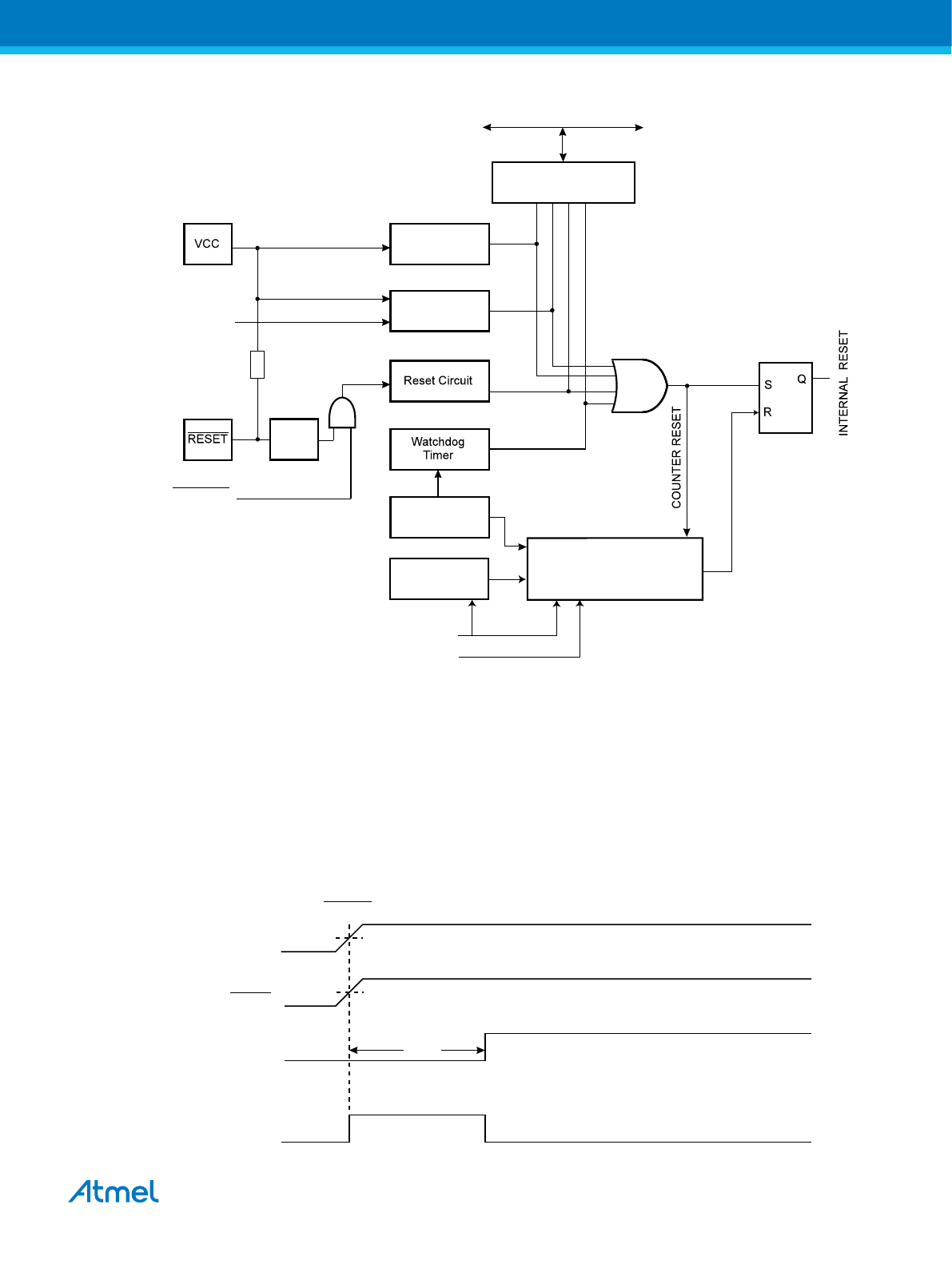
Figure 15-1. Reset Logic
MCU Status
Register (MCUSR)
Brown-out
Reset Circuit
BODLEVEL [2..0]
Delay Counters
CKSEL[3:0]
CK
TIMEOUT
WDRF
BORF
EXTRF
PORF
DATA BUS
Clock
Generator
SPIKE
FILTER
Pull-up Resistor
Watchdog
Oscillator
SUT[1:0]
Power-on Reset
Circuit
RSTDISBL
15.3. Power-on Reset
A Power-on Reset (POR) pulse is generated by an On-chip detection circuit. The POR is activated
whenever V
CC
is below the detection level. The POR circuit can be used to trigger the start-up Reset, as
well as to detect a failure in supply voltage.
A Power-on Reset (POR) circuit ensures that the device is reset from Power-on. Reaching the Power-on
Reset threshold voltage invokes the delay counter, which determines how long the device is kept in Reset
after V
CC
rise. The Reset signal is activated again, without any delay, when V
CC
decreases below the
detection level.
Figure 15-2. MCU Start-up,
RESET Tied to V
CC
V
RESET
TIME-OUT
INTERNAL
RESET
t
TOUT
V
POT
V
RST
CC
Atmel ATmega328/P [DATASHEET]
Atmel-42735B-ATmega328/P_Datasheet_Complete-11/2016
73
Page 74
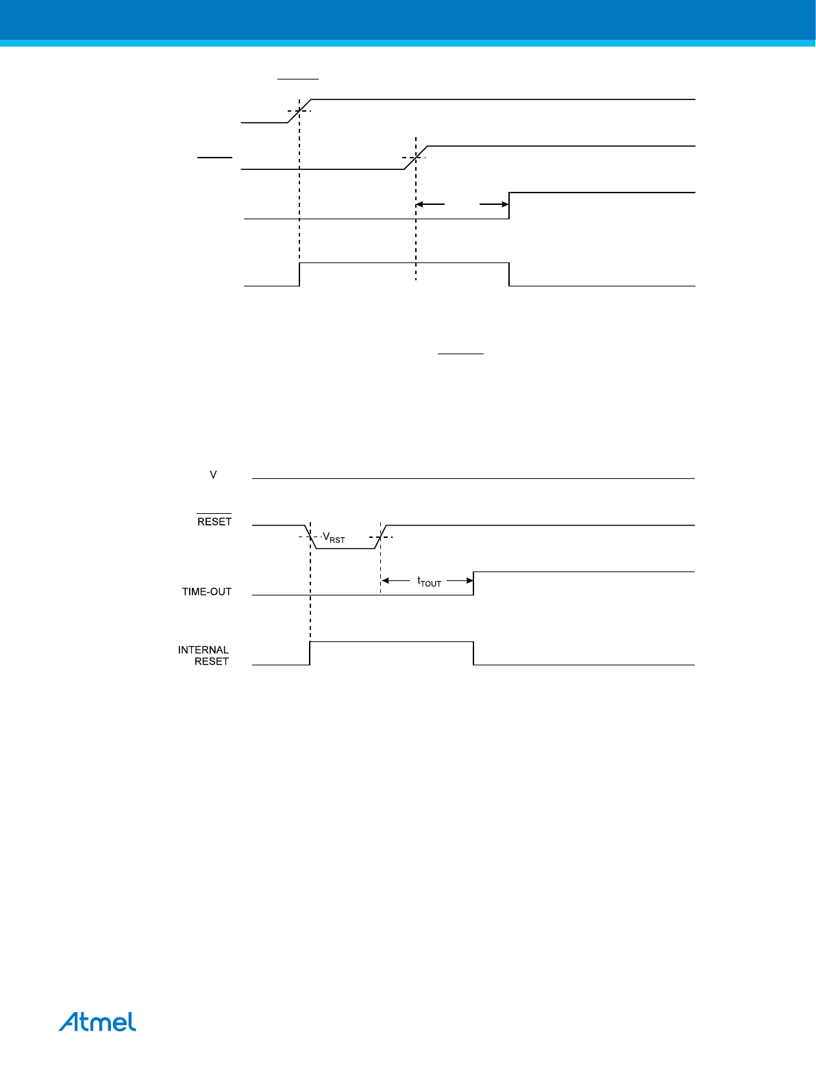
Figure 15-3. MCU Start-up, RESET Extended Externally
RESET
TIME-OUT
INTERNAL
RESET
t
TOUT
V
POT
V
RST
V
CC
15.4. External Reset
An External Reset is generated by a low level on the RESET pin. Reset pulses longer than the minimum
pulse width will generate a reset, even if the clock is not running. Shorter pulses are not guaranteed to
generate a reset. When the applied signal reaches the Reset Threshold Voltage (V
RST
) on its positive
edge, the delay counter starts the MCU after the Time-out period (t
TOUT
) has expired. The External Reset
can be disabled by the RSTDISBL fuse.
Figure 15-4. External Reset During Operation
CC
15.5. Brown-out Detection
The device has an On-chip Brown-out Detection (BOD) circuit for monitoring the V
CC
level during
operation by comparing it to a fixed trigger level. The trigger level for the BOD can be selected by the
BODLEVEL Fuses. The trigger level has a hysteresis to ensure spike free Brown-out Detection. The
hysteresis on the detection level should be interpreted as V
BOT+
= V
BOT
+ V
HYST
/2 and V
BOT-
= V
BOT
-
V
HYST
/2. When the BOD is enabled, and V
CC
decreases to a value below the trigger level (V
BOT-
in the
following figure), the Brown-out Reset is immediately activated. When V
CC
increases above the trigger
level (V
BOT+
in the following figure), the delay counter starts the MCU after the Time-out period t
TOUT
has
expired.
The BOD circuit will only detect a drop in V
CC
if the voltage stays below the trigger level for longer than
t
BOD
.
Atmel ATmega328/P [DATASHEET]
Atmel-42735B-ATmega328/P_Datasheet_Complete-11/2016
74
Page 75
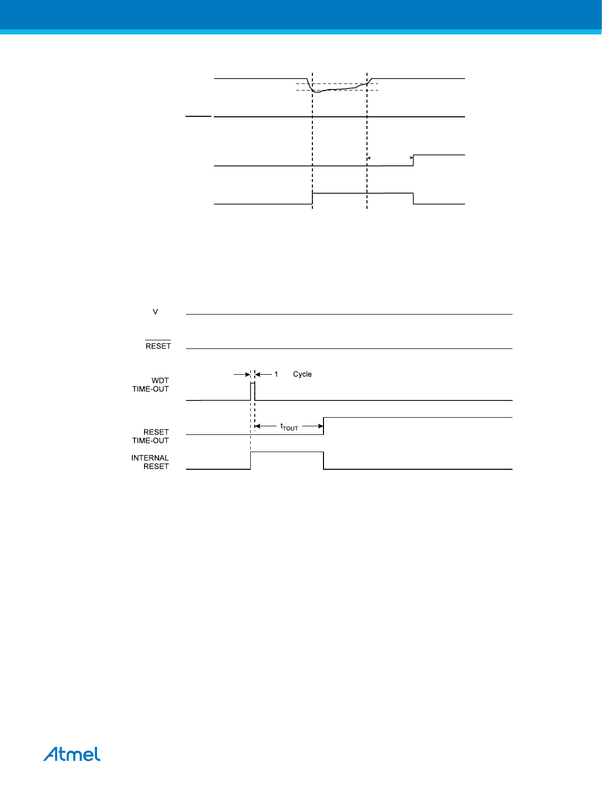
Figure 15-5. Brown-out Reset During Operation
V
CC
RESET
TIME-OUT
INTERNAL
RESET
V
BOT-
V
BOT+
t
TOUT
15.6. Watchdog System Reset
When the Watchdog times out, it will generate a short reset pulse of one CK cycle duration. On the falling
edge of this pulse, the delay timer starts counting the Time-out period t
TOUT
.
Figure 15-6. Watchdog System Reset During Operation
CK
CC
15.7. Internal Voltage Reference
The device features an internal bandgap reference. This reference is used for Brown-out Detection, and it
can be used as an input to the Analog Comparator or the ADC.
15.7.1. Voltage Reference Enable Signals and Start-up Time
The voltage reference has a start-up time that may influence the way it should be used. To save power,
the reference is not always turned on. The reference is on during the following situations:
1. When the BOD is enabled (by programming the BODLEVEL [2:0] Fuses).
2. When the bandgap reference is connected to the Analog Comparator (by setting the ACBG bit in
ACSR (ACSR.ACBG)).
3. When the ADC is enabled.
Thus, when the BOD is not enabled, after setting ACSR.ACBG or enabling the ADC, the user must
always allow the reference to start up before the output from the Analog Comparator or ADC is used. To
reduce power consumption in Power-Down mode, the user can avoid the three conditions above to
ensure that the reference is turned off before entering Power-Down mode.
Atmel ATmega328/P [DATASHEET]
Atmel-42735B-ATmega328/P_Datasheet_Complete-11/2016
75
Page 76
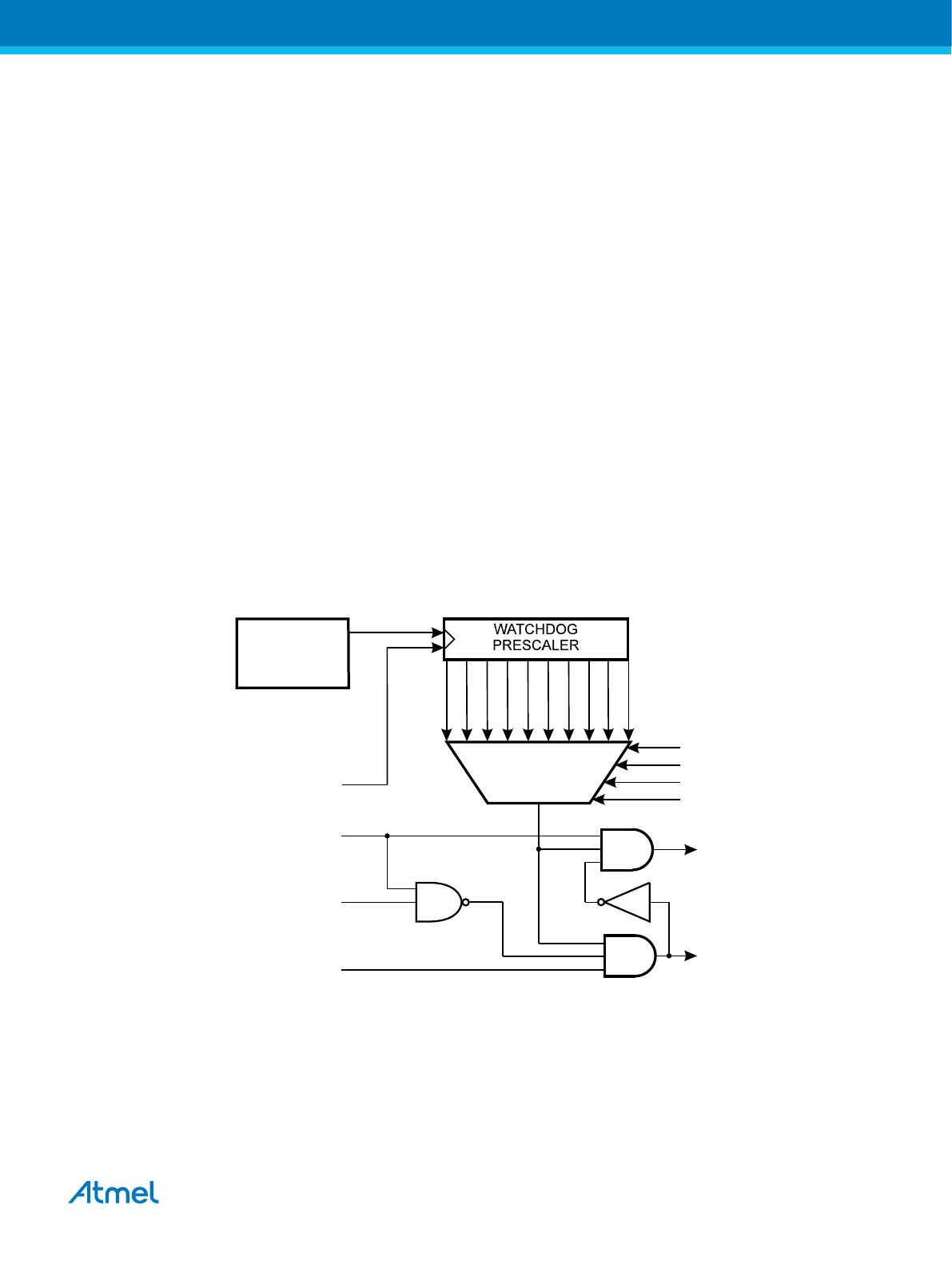
15.8. Watchdog Timer
If the watchdog timer is not needed in the application, the module should be turned off. If the watchdog
timer is enabled, it will be enabled in all sleep modes and hence always consume power. In the deeper
sleep modes, this will contribute significantly to the total current consumption.
Refer to Watchdog System Reset for details on how to configure the watchdog timer.
15.8.1. Features
• Clocked from separate On-chip Oscillator
• Three operating modes:
– Interrupt
– System Reset
– Interrupt and System Reset
• Selectable Time-out period from 16ms to 8s
• Possible Hardware fuse Watchdog always on (WDTON) for fail-safe mode
15.8.2. Overview
The device has an Enhanced Watchdog Timer (WDT). The WDT is a timer counting cycles of a separate
on-chip 128kHz oscillator. The WDT gives an interrupt or a system reset when the counter reaches a
given time-out value. In normal operation mode, it is required that the system uses the Watchdog Timer
Reset (WDR) instruction to restart the counter before the time-out value is reached. If the system doesn't
restart the counter, an interrupt or system reset will be issued.
Figure 15-7. Watchdog Timer
128kHz
OSCILLATOR
OSC/2K
OSC/4K
OSC/8K
OSC/16K
OSC/32K
OSC/64K
OSC/128K
OSC/256K
OSC/512K
OSC/1024K
WDP0
WDP1
WDP2
WDP3
WATCHDOG
RESET
WDE
WDIF
WDIE
MCU RESET
INTERRUPT
In Interrupt mode, the WDT gives an interrupt when the timer expires. This interrupt can be used to wake
the device from sleep-modes, and also as a general system timer. One example is to limit the maximum
time allowed for certain operations, giving an interrupt when the operation has run longer than expected.
In System Reset mode, the WDT gives a reset when the timer expires. This is typically used to prevent
system hang-up in case of runaway code. The third mode, Interrupt and System Reset mode, combines
the other two modes by first giving an interrupt and then switch to System Reset mode. This mode will for
instance allow a safe shutdown by saving critical parameters before a system reset.
Atmel ATmega328/P [DATASHEET]
Atmel-42735B-ATmega328/P_Datasheet_Complete-11/2016
76
Page 77

The Watchdog always on (WDTON) fuse, if programmed, will force the Watchdog Timer to System Reset
mode. With the fuse programmed the System Reset mode bit (WDE) and Interrupt mode bit (WDIE) are
locked to 1 and 0 respectively. To further ensure program security, alterations to the Watchdog set-up
must follow timed sequences. The sequence for clearing WDE and changing time-out configuration is as
follows:
1. In the same operation, write a logic one to the Watchdog change enable bit (WDCE) and Watchdog
System Reset Enable (WDE) in Watchdog Timer Control Register (WDTCSR.WDCE and
WDTCSR.WDE). A logic one must be written to WDTCSR.WDE regardless of the previous value of
the WDTCSR.WDE.
2. Within the next four clock cycles, write the WDTCSR.WDE and Watchdog prescaler bits group
(WDTCSR.WDP) as desired, but with the WDTCSR.WDCE cleared. This must be done in one
operation.
The following examples show a function for turning off the Watchdog Timer. The
examples assume that interrupts are controlled (e.g. by disabling interrupts globally) so
that no interrupts will occur during the execution of these functions.
Assembly Code Example
WDT_off:
; Turn off global interrupt
cli
; Reset Watchdog Timer
wdr
; Clear WDRF in MCUSR
in r16, MCUSR
andi r16, (0xff & (0<<WDRF))
out MCUSR, r16
; Write '1' to WDCE and WDE
; Keep old prescaler setting to prevent unintentional time-out
lds r16, WDTCSR
ori r16, (1<<WDCE) | (1<<WDE)
sts WDTCSR, r16
; Turn off WDT
ldi r16, (0<<WDE)
sts WDTCSR, r16
; Turn on global interrupt
sei
ret
C Code Example
void WDT_off(void)
{
__disable_interrupt();
__watchdog_reset();
/* Clear WDRF in MCUSR */
MCUSR &= ~(1<<WDRF);
/* Write logical one to WDCE and WDE */
/* Keep old prescaler setting to prevent unintentional time-out */
WDTCSR |= (1<<WDCE) | (1<<WDE);
/* Turn off WDT */
WDTCSR = 0x00;
__enable_interrupt();
}
Note: If the Watchdog is accidentally enabled, for example by a runaway pointer or
brown-out condition, the device will be reset and the Watchdog Timer will stay enabled. If
the code is not set up to handle the Watchdog, this might lead to an eternal loop of time-
out resets. To avoid this situation, the application software should always clear the
Watchdog System Reset Flag (WDRF) and the WDE control bit in the initialization
routine, even if the Watchdog is not in use.
Atmel ATmega328/P [DATASHEET]
Atmel-42735B-ATmega328/P_Datasheet_Complete-11/2016
77
Page 78

The following code examples shows how to change the time-out value of the Watchdog
Timer.
Assembly Code Example
WDT_Prescaler_Change:
; Turn off global interrupt
cli
; Reset Watchdog Timer
wdr
; Start timed sequence
lds r16, WDTCSR
ori r16, (1<<WDCE) | (1<<WDE)
sts WDTCSR, r16
; -- Got four cycles to set the new values from here -
; Set new prescaler(time-out) value = 64K cycles (~0.5 s)
ldi r16, (1<<WDE) | (1<<WDP2) | (1<<WDP0)
sts WDTCSR, r16
; -- Finished setting new values, used 2 cycles -
; Turn on global interrupt
sei
ret
C Code Example
void WDT_Prescaler_Change(void)
{
__disable_interrupt();
__watchdog_reset();
/* Start timed sequence */
WDTCSR |= (1<<WDCE) | (1<<WDE);
/* Set new prescaler(time-out) value = 64K cycles (~0.5 s) */
WDTCSR = (1<<WDE) | (1<<WDP2) | (1<<WDP0);
__enable_interrupt();
}
Note: The Watchdog Timer should be reset before any change of the WDTCSR.WDP
bits, since a change in the WDTCSR.WDP bits can result in a time-out when switching to
a shorter time-out period.
15.9. Register Description
Atmel ATmega328/P [DATASHEET]
Atmel-42735B-ATmega328/P_Datasheet_Complete-11/2016
78
Page 79
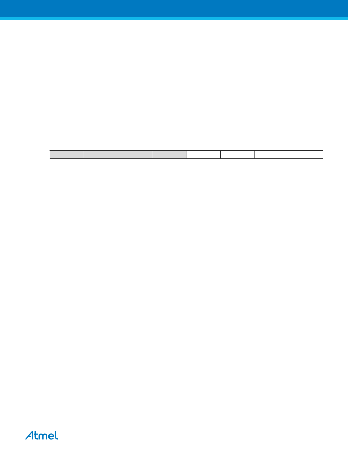
15.9.1. MCU Status Register
To make use of the Reset Flags to identify a reset condition, the user should read and then Reset the
MCUSR as early as possible in the program. If the register is cleared before another reset occurs, the
source of the reset can be found by examining the Reset Flags.
When addressing I/O Registers as data space using LD and ST instructions, the provided offset must be
used. When using the I/O specific commands IN and OUT, the offset is reduced by 0x20, resulting in an
I/O address offset within 0x00 - 0x3F.
Name: MCUSR
Offset: 0x54
Reset: 0x00
Property:
When addressing as I/O Register: address offset is 0x34
Bit 7 6 5 4 3 2 1 0
WDRF BORF EXTRF PORF
Access
R/W R/W R/W R/W
Reset 0 0 0 0
Bit 3 – WDRF: Watchdog System Reset Flag
This bit is set if a Watchdog System Reset occurs. The bit is reset by a Power-on Reset, or by writing a '0'
to it.
Bit 2 – BORF: Brown-out Reset Flag
This bit is set if a Brown-out Reset occurs. The bit is reset by a Power-on Reset, or by writing a '0' to it.
Bit 1 – EXTRF: External Reset Flag
This bit is set if an External Reset occurs. The bit is reset by a Power-on Reset, or by writing a '0' to it.
Bit 0 – PORF: Power-on Reset Flag
This bit is set if a Power-on Reset occurs. The bit is reset only by writing a '0' to it.
Atmel ATmega328/P [DATASHEET]
Atmel-42735B-ATmega328/P_Datasheet_Complete-11/2016
79
Page 80
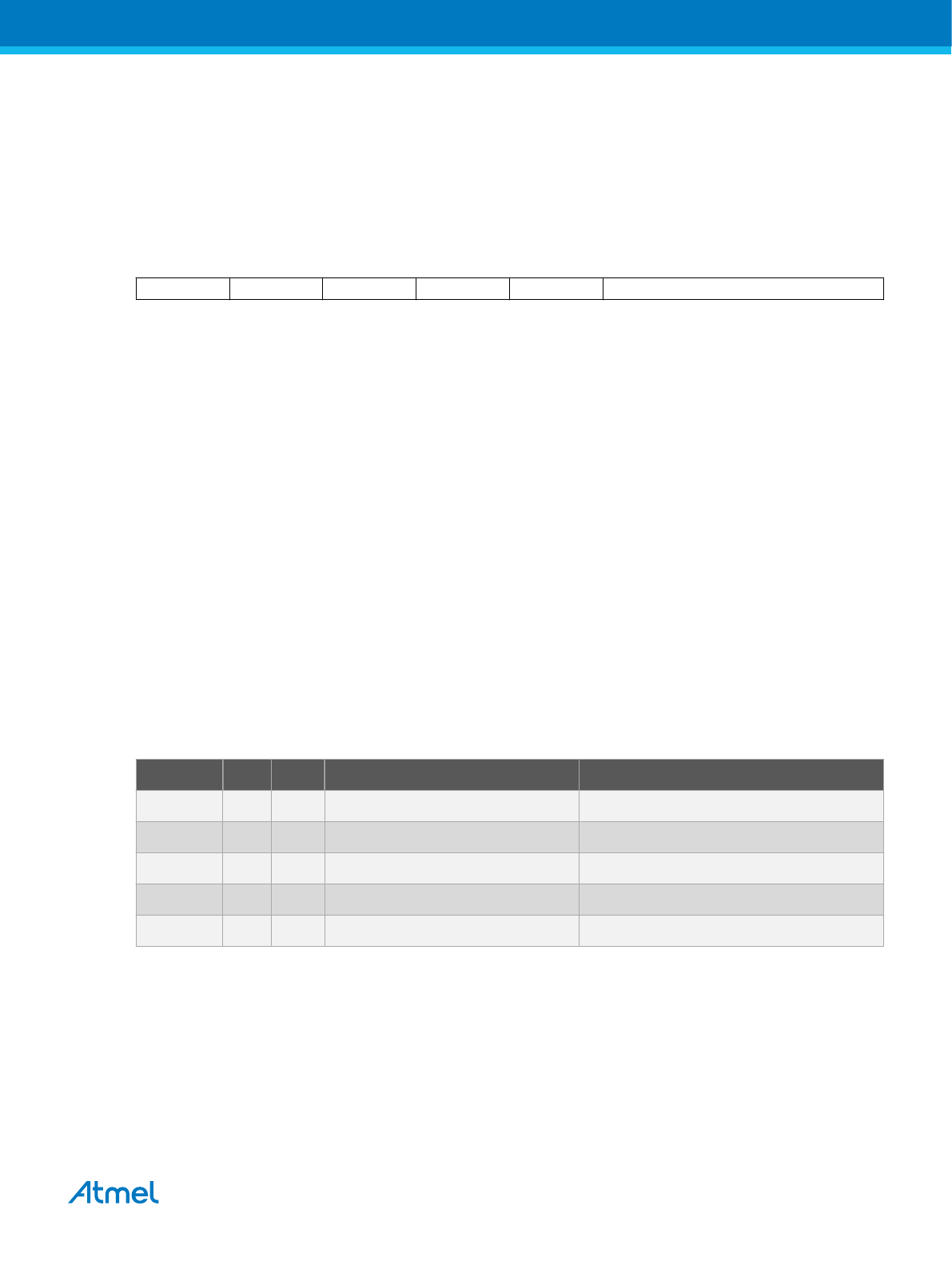
15.9.2. WDTCSR – Watchdog Timer Control Register
Name: WDTCSR
Offset: 0x60
Reset: 0x00
Property:
Bit 7 6 5 4 3 2 1 0
WDIF WDIE WDP[3] WDCE WDE WDP[2:0]
Access
R/W R/W R/W R/W R/W R/W R/W R/W
Reset 0 0 0 0 0 0 0 0
Bit 7 – WDIF: Watchdog Interrupt Flag
This bit is set when a timeout occurs in the Watchdog Timer and the Watchdog Timer is configured for
interrupt. WDIF is cleared by hardware when executing the corresponding interrupt handling vector.
Alternatively, WDIF is cleared by writing a '1' to it. When the I-bit in SREG and WDIE are set, the
Watchdog Timeout Interrupt is executed.
Bit 6 – WDIE: Watchdog Interrupt Enable
When this bit is written to '1' and the I-bit in the Status Register is set, the Watchdog Interrupt is enabled.
If WDE is cleared in combination with this setting, the Watchdog Timer is in Interrupt Mode, and the
corresponding interrupt is executed if timeout in the Watchdog Timer occurs. If WDE is set, the Watchdog
Timer is in Interrupt and System Reset Mode. The first timeout in the Watchdog Timer will set WDIF.
Executing the corresponding interrupt vector will clear WDIE and WDIF automatically by hardware (the
Watchdog goes to System Reset Mode).
This is useful for keeping the Watchdog Timer security while using the interrupt. To stay in Interrupt and
System Reset Mode, WDIE must be set after each interrupt. This should however not be done within the
interrupt service routine itself, as this might compromise the safety function of the Watchdog System
Reset mode. If the interrupt is not executed before the next timeout, a System Reset will be applied.
Table 15-1. Watchdog Timer Configuration
WDTON
(1)
WDE WDIE Mode Action on Time-out
1 0 0 Stopped None
1 0 1 Interrupt Mode Interrupt
1 1 0 System Reset Mode Reset
1 1 1 Interrupt and System Reset Mode Interrupt, then go to System Reset Mode
0 x x System Reset Mode Reset
Note: 1. WDTON Fuse set to '0' means programmed and '1' means unprogrammed.
Bit 5 – WDP[3]: Watchdog Timer Prescaler 3
Bit 4 – WDCE: Watchdog Change Enable
This bit is used in timed sequences for changing WDE and prescaler bits. To clear the WDE bit, and/or
change the prescaler bits, WDCE must be set. Once written to '1', hardware will clear WDCE after four
clock cycles.
Atmel ATmega328/P [DATASHEET]
Atmel-42735B-ATmega328/P_Datasheet_Complete-11/2016
80
Page 81
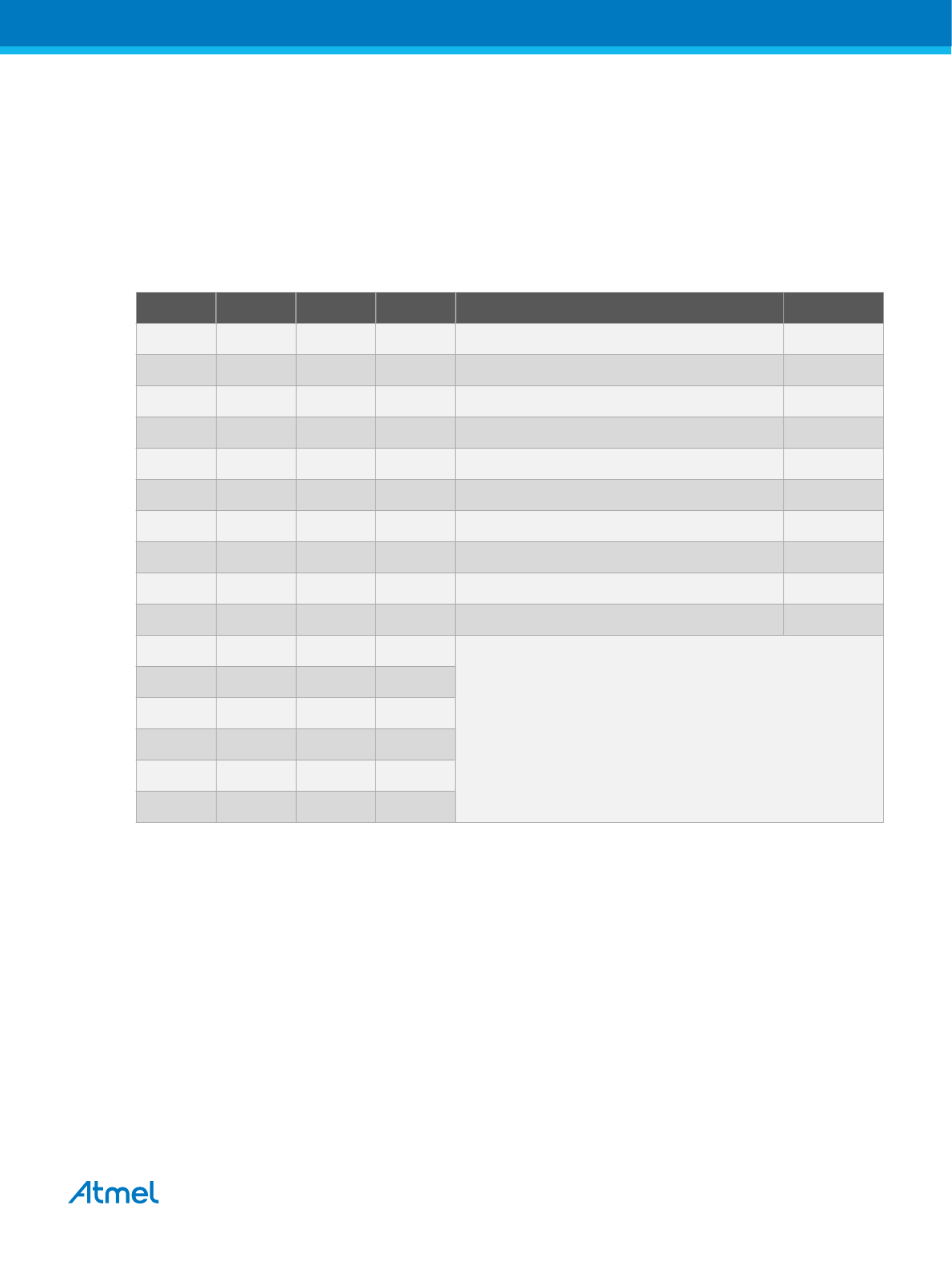
Bit 3 – WDE: Watchdog System Reset Enable
WDE is overridden by WDRF in MCUSR. This means that WDE is always set when WDRF is set. To
clear WDE, WDRF must be cleared first. This feature ensures multiple resets during conditions causing
failure, and a safe startup after the failure.
Bits 2:0 – WDP[2:0]: Watchdog Timer Prescaler 2, 1, and 0
The WDP[3:0] bits determine the Watchdog Timer prescaling when the Watchdog Timer is running. The
different prescaling values and their corresponding timeout periods are shown in the following table.
Table 15-2. Watchdog Timer Prescale Select
WDP[3] WDP[2] WDP[1] WDP[0] Number of WDT Oscillator (Cycles) Oscillator
0 0 0 0 2K (2048) 16ms
0 0 0 1 4K (4096) 32ms
0 0 1 0 8K (8192) 64ms
0 0 1 1 16K (16384) 0.125s
0 1 0 0 32K (32768) 0.25s
0 1 0 1 64K (65536) 0.5s
0 1 1 0 128K (131072) 1.0s
0 1 1 1 256K (262144) 2.0s
1 0 0 0 512K (524288) 4.0s
1 0 0 1 1024K (1048576) 8.0s
1 0 1 0 Reserved
1 0 1 1
1 1 0 0
1 1 0 1
1 1 1 0
1 1 1 1
Atmel ATmega328/P [DATASHEET]
Atmel-42735B-ATmega328/P_Datasheet_Complete-11/2016
81
Page 82
16. Interrupts
This section describes the specifics of the interrupt handling of the device. For a general explanation of
the AVR interrupt handling, refer to the description of Reset and Interrupt Handling.
• Each Interrupt Vector occupies two instruction words .
• Reset Vector is affected by the BOOTRST fuse, and the Interrupt Vector start address is affected by
the IVSEL bit in MCUCR
16.1. Interrupt Vectors in ATmega328/P
Table 16-1. Reset and Interrupt Vectors in ATmega328/P
Vector No
Program Address
(2)
Source Interrupts definition
1 0x0000
(1)
RESET External Pin, Power-on Reset, Brown-out Reset and Watchdog System
Reset
2 0x0002 INT0 External Interrupt Request 0
3 0x0004 INT1 External Interrupt Request 0
4 0x0006 PCINT0 Pin Change Interrupt Request 0
5 0x0008 PCINT1 Pin Change Interrupt Request 1
6 0x000A PCINT2 Pin Change Interrupt Request 2
7 0x000C WDT Watchdog Time-out Interrupt
8 0x000E TIMER2_COMPA Timer/Counter2 Compare Match A
9 0x0010 TIMER2_COMPB Timer/Coutner2 Compare Match B
10 0x0012 TIMER2_OVF Timer/Counter2 Overflow
11 0x0014 TIMER1_CAPT Timer/Counter1 Capture Event
12 0x0016 TIMER1_COMPA Timer/Counter1 Compare Match A
13 0x0018 TIMER1_COMPB Timer/Coutner1 Compare Match B
14 0x001A TIMER1_OVF Timer/Counter1 Overflow
15 0x001C TIMER0_COMPA Timer/Counter0 Compare Match A
16 0x001E TIMER0_COMPB Timer/Coutner0 Compare Match B
17 0x0020 TIMER0_OVF Timer/Counter0 Overflow
18 0x0022 SPI STC SPI Serial Transfer Complete
19 0x0024 USART_RX USART Rx Complete
20 0x0026 USART_UDRE USART Data Register Empty
21 0x0028 USART_TX USART Tx Complete
22 0x002A ADC ADC Conversion Complete
23 0x002C EE READY EEPROM Ready
24 0x002E ANALOG COMP Analog Comparator
Atmel ATmega328/P [DATASHEET]
Atmel-42735B-ATmega328/P_Datasheet_Complete-11/2016
82
Page 83

Vector No Program Address
(2)
Source Interrupts definition
25 0x0030 TWI 2-wire Serial Interface (I
2
C)
26 0x0032 SPM READY Store Program Memory Ready
Note:
1. When the BOOTRST Fuse is programmed, the device will jump to the Boot Loader address at
reset, see ”Boot Loader Support – Read-While-Write Self- Programming”
2. When the IVSEL bit in MCUCR is set, Interrupt Vectors will be moved to the start of the Boot Flash
Section. The address of each Interrupt Vector will then be the address in this table added to the
start address of the Boot Flash Section.
The table below shows reset and Interrupt Vectors placement for the various combinations of BOOTRST
and IVSEL settings. If the program never enables an interrupt source, the Interrupt Vectors are not used,
and regular program code can be placed at these locations. This is also the case if the Reset Vector is in
the Application section while the Interrupt Vectors are in the Boot section or vice versa.
Table 16-2. Reset and Interrupt Vectors Placement
BOOTRST
(1)
IVSEL Reset Address Interrupt Vectors Start Address
1 0 0x000 0x002
1 1 0x000 Boot Reset Address + 0x0002
0 0 Boot Reset Address 0x002
0 1 Boot Reset Address Boot Reset Address + 0x0002
Note: 1. For the BOOTRST Fuse “1” means unprogrammed while “0” means programmed.
The most typical and general program setup for the Reset and Interrupt Vector Addresses is:
Address Labels Code Comments
0x0000 jmp RESET ; Reset
0x0002 jmp INT0 ; IRQ0
0x0004 jmp INT1 ; IRQ1
0x0006 jmp PCINT0 ; PCINT0
0x0008 jmp PCINT1 ; PCINT1
0x000A jmp PCINT2 ; PCINT2
0x000C jmp WDT ; Watchdog Timeout
0x000E jmp TIM2_COMPA ; Timer2 CompareA
0x0010 jmp TIM2_COMPB ; Timer2 CompareB
0x0012 jmp TIM2_OVF ; Timer2 Overflow
0x0014 jmp TIM1_CAPT ; Timer1 Capture
0x0016 jmp TIM1_COMPA ; Timer1 CompareA
0x0018 jmp TIM1_COMPB ; Timer1 CompareB
0x001A jmp TIM1_OVF ; Timer1 Overflow
0x001C jmp TIM0_COMPA ; Timer0 CompareA
0x001E jmp TIM0_COMPB ; Timer0 CompareB
0x0020 jmp TIM0_OVF ; Timer0 Overflow
0x0022 jmp SPI_STC ; SPI Transfer Complete
0x0024 jmp USART_RXC ; USART RX Complete
0x0026 jmp USART_UDRE ; USART UDR Empty
0x0028 jmp USART_TXC ; USART TX Complete
0x002A jmp ADC ; ADC Conversion Complete
0x002C jmp EE_RDY ; EEPROM Ready
0x002E jmp ANA_COMP ; Analog Comparator
0x0030 jmp TWI ; 2-wire Serial
0x0032 jmp SPM_RDY ; SPM Ready
;
0x0034 RESET: ldi r16,high(RAMEND) ; Main program start
0x0035 out SPH,r16 ; Set Stack Pointer to top of RAM
0x0036 ldi r16,low(RAMEND)
0x0037 out SPL,r16
0x0038 sei ; Enable interrupts
Atmel ATmega328/P [DATASHEET]
Atmel-42735B-ATmega328/P_Datasheet_Complete-11/2016
83
Page 84

0x0039 <instr> xxx
... ... ... ...
When the BOOTRST Fuse is unprogrammed, the Boot section size set to 2Kbytes and the
MCUCR.IVSEL is set before any interrupts are enabled, the most typical and general program setup for
the Reset and Interrupt Vector Addresses is:
Address Labels Code Comments
0x0000 RESET: ldi r16,high(RAMEND) ; Main program start
0x0001 out SPH,r16 ; Set Stack Pointer to top of RAM
0x0002 ldi r16,low(RAMEND)
0x0003 out SPL,r16
0x0004 sei ; Enable interrupts
0x0005 <instr> xxx
;
.org 0x3C02
0x3C02 jmp EXT_INT0 ; IRQ0 Handler
0x3C04 jmp EXT_INT1 ; IRQ1 Handler
... ... ... ;
0x3C32 jmp SPM_RDY ; SPM Ready Handler
When the BOOTRST Fuse is programmed and the Boot section size set to 2Kbytes, the most typical and
general program setup for the Reset and Interrupt Vector Addresses is:
Address Labels Code Comments
.org 0x0002
0x0002 jmp EXT_INT0 ; IRQ0 Handler
0x0004 jmp EXT_INT1 ; IRQ1 Handler
... ... ... ;
0x0032 jmp SPM_RDY ; SPM Ready Handler
;
.org 0x3C00
0x3C00 RESET: ldi r16,high(RAMEND) ; Main program start
0x3C01 out SPH,r16 ; Set Stack Pointer to top of RAM
0x3C02 ldi r16,low(RAMEND)
0x3C03 out SPL,r16
0x3C04 sei ; Enable interrupts
0x3C05 <instr> xxx
When the BOOTRST Fuse is programmed, the Boot section size set to 2K bytes and the MCUCR.IVSEL
is set before any interrupts are enabled, the most typical and general program setup for the Reset and
Interrupt Vector Addresses is:
Address Labels Code Comments
;
.org 0x3C00
0x3C00 jmp RESET ; Reset handler
0x3C02 jmp EXT_INT0 ; IRQ0 Handler
0x3C04 jmp EXT_INT1 ; IRQ1 Handler
... ... ... ;
0x3C32 jmp SPM_RDY ; SPM Ready Handler
;
0x3C34 RESET: ldi r16,high(RAMEND) ; Main program start
0x3C35 out SPH,r16 ; Set Stack Pointer to top of RAM
0x3C36 ldi r16,low(RAMEND)
0x3C37 out SPL,r16
0x3C38 sei ; Enable interrupts
0x3C39 <instr> xxx
16.2. Register Description
16.2.1. Moving Interrupts Between Application and Boot Space
The MCU Control Register controls the placement of the Interrupt Vector table.
Atmel ATmega328/P [DATASHEET]
Atmel-42735B-ATmega328/P_Datasheet_Complete-11/2016
84
Page 85
16.2.2. MCU Control Register
When addressing I/O Registers as data space using LD and ST instructions, the provided offset must be
used. When using the I/O specific commands IN and OUT, the offset is reduced by 0x20, resulting in an
I/O address offset within 0x00 - 0x3F.
Name: MCUCR
Offset: 0x55
Reset: 0x00
Property:
When addressing as I/O Register: address offset is 0x35
Bit 7 6 5 4 3 2 1 0
BODS BODSE PUD IVSEL IVCE
Access
R/W R/W R/W R/W R/W
Reset 0 0 0 0 0
Bit 6 – BODS: BOD Sleep
The BODS bit must be written to '1' in order to turn off BOD during sleep. Writing to the BODS bit is
controlled by a timed sequence and the enable bit BODSE. To disable BOD in relevant sleep modes, both
BODS and BODSE must first be written to '1'. Then, BODS must be written to '1' and BODSE must be
written to zero within four clock cycles.
The BODS bit is active three clock cycles after it is set. A sleep instruction must be executed while BODS
is active in order to turn off the BOD for the actual sleep mode. The BODS bit is automatically cleared
after three clock cycles.
Note: BOD disable is only available for ATmega328P.
Bit 5 – BODSE: BOD Sleep Enable
BODSE enables setting of BODS control bit, as explained in BODS bit description. BOD disable is
controlled by a timed sequence.
Note: BOD disable is only available for ATmega328P.
Bit 4 – PUD: Pull-up Disable
When this bit is written to one, the pull-ups in the I/O ports are disabled even if the DDxn and PORTxn
Registers are configured to enable the pull-ups ({DDxn, PORTxn} = 0b01).
Bit 1 – IVSEL: Interrupt Vector Select
When the IVSEL bit is cleared (zero), the Interrupt Vectors are placed at the start of the Flash memory.
When this bit is set (one), the Interrupt Vectors are moved to the beginning of the Boot Loader section of
the Flash. The actual address of the start of the Boot Flash Section is determined by the BOOTSZ Fuses.
To avoid unintentional changes of Interrupt Vector tables, a special write procedure must be followed to
change the IVSEL bit:
1. Write the Interrupt Vector Change Enable (IVCE) bit to one.
2. Within four cycles, write the desired value to IVSEL while writing a zero to IVCE.
Interrupts will automatically be disabled while this sequence is executed. Interrupts are disabled in the
cycle IVCE is set, and they remain disabled until after the instruction following the write to IVSEL. If
IVSEL is not written, interrupts remain disabled for four cycles. The I-bit in the Status Register is
unaffected by the automatic disabling.
Atmel ATmega328/P [DATASHEET]
Atmel-42735B-ATmega328/P_Datasheet_Complete-11/2016
85
Page 86

Note: If Interrupt Vectors are placed in the Boot Loader section and Boot Lock bit BLB02 is
programmed, interrupts are disabled while executing from the Application section. If Interrupt Vectors are
placed in the Application section and Boot Lock bit BLB12 is programed, interrupts are disabled while
executing from the Boot Loader section.
Bit 0 – IVCE: Interrupt Vector Change Enable
The IVCE bit must be written to logic one to enable change of the IVSEL bit. IVCE is cleared by hardware
four cycles after it is written or when IVSEL is written. Setting the IVCE bit will disable interrupts, as
explained in the IVSEL description above. See Code Example below.
Assembly Code Example
Move_interrupts:
; Get MCUCR
in r16, MCUCR
mov r17, r16
; Enable change of Interrupt Vectors
ori r16, (1<<IVCE)
out MCUCR, r16
; Move interrupts to Boot Flash section
ori r17, (1<<IVSEL)
out MCUCR, r17
ret
C Code Example
void Move_interrupts(void)
{
uchar temp;
/* GET MCUCR*/
temp = MCUCR;
/* Enable change of Interrupt Vectors */
MCUCR = temp|(1<<IVCE);
/* Move interrupts to Boot Flash section */
MCUCR = temp|(1<<IVSEL);
}
Atmel ATmega328/P [DATASHEET]
Atmel-42735B-ATmega328/P_Datasheet_Complete-11/2016
86
Page 87

17. EXINT - External Interrupts
The External Interrupts are triggered by the INT pins or any of the PCINT pins. Observe that, if enabled,
the interrupts will trigger even if the INT or PCINT pins are configured as outputs. This feature provides a
way of generating a software interrupt.
The Pin Change Interrupt Request 2 (PCI2) will trigger if any enabled PCINT[23:16] pin toggles. The Pin
Change Interrupt Request 1 (PCI1) will trigger if any enabled PCINT[14:8] pin toggles. The Pin Change
Interrupt Request 0 (PCI0) will trigger if any enabled PCINT[7:0] pin toggles. The PCMSK2, PCMSK1 and
PCMSK0 Registers control which pins contribute to the pin change interrupts. Pin change interrupts on
PCINT are detected asynchronously. This implies that these interrupts can be used for waking the part
also from sleep modes other than Idle mode.
The External Interrupts can be triggered by a falling or rising edge or a low level. This is set up as
indicated in the specification for the External Interrupt Control Register A (EICRA). When the External
Interrupts are enabled and are configured as level triggered, the interrupts will trigger as long as the pin is
held low. Note that recognition of falling or rising edge interrupts on INT requires the presence of an I/O
clock. Low level interrupt on INT is detected asynchronously. This implies that this interrupt can be used
for waking the part also from sleep modes other than Idle mode. The I/O clock is halted in all sleep modes
except Idle mode.
Note: If a level triggered interrupt is used for wake-up from Power-down, the required level must be held
long enough for the MCU to complete the wake-up to trigger the level interrupt. If the level disappears
before the end of the Start-up Time, the MCU will still wake up, but no interrupt will be generated. The
start-up time is defined by the SUT and CKSEL Fuses.
Related Links
System Control and Reset on page 72
Clock Systems and Their Distribution on page 48
System Clock and Clock Options on page 48
17.1. Pin Change Interrupt Timing
An example of timing of a pin change interrupt is shown in the following figure.
Atmel ATmega328/P [DATASHEET]
Atmel-42735B-ATmega328/P_Datasheet_Complete-11/2016
87
Page 88
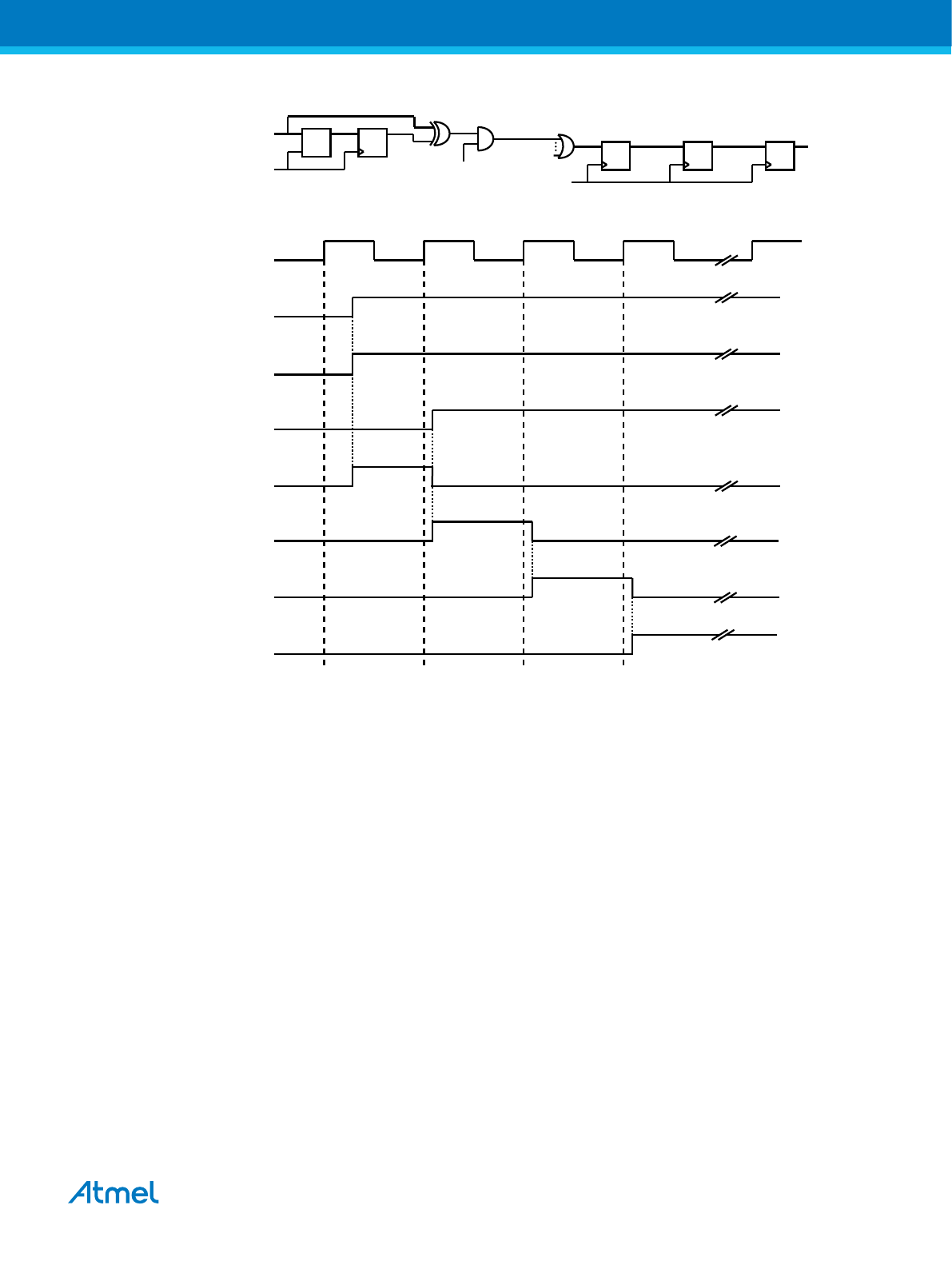
Figure 17-1. Timing of pin change interrupts
clk
PCINT(0)
pin_lat
pin_sync
pcint_in_(0)
pcint_syn
pcint_setflag
PCIF
PCINT(0)
pin_sync
pcint_syn
pin_lat
D Q
LE
pcint_setflag
PCIF
clk
clk
PCINT(0) in PCMSK(x)
pcint_in_(0)
0
x
Related Links
System Control and Reset on page 72
Clock Systems and Their Distribution on page 48
System Clock and Clock Options on page 48
17.2. Register Description
Atmel ATmega328/P [DATASHEET]
Atmel-42735B-ATmega328/P_Datasheet_Complete-11/2016
88
Page 89
17.2.1. External Interrupt Control Register A
The External Interrupt Control Register A contains control bits for interrupt sense control.
Name: EICRA
Offset: 0x69
Reset: 0x00
Property:
-
Bit 7 6 5 4 3 2 1 0
ISC11 ISC10 ISC01 ISC00
Access
R/W R/W R/W R/W
Reset 0 0 0 0
Bits 3:2 – ISC1n: Interrupt Sense Control 1 [n = 1:0]
The External Interrupt 1 is activated by the external pin INT1 if the SREG I-flag and the corresponding
interrupt mask are set. The level and edges on the external INT1 pin that activate the interrupt are defined
in the table below. The value on the INT1 pin is sampled before detecting edges. If edge or toggle
interrupt is selected, pulses that last longer than one clock period will generate an interrupt. Shorter
pulses are not guaranteed to generate an interrupt. If low level interrupt is selected, the low level must be
held until the completion of the currently executing instruction to generate an interrupt.
Value Description
00 The low level of INT1 generates an interrupt request.
01 Any logical change on INT1 generates an interrupt request.
10 The falling edge of INT1 generates an interrupt request.
11 The rising edge of INT1 generates an interrupt request.
Bits 1:0 – ISC0n: Interrupt Sense Control 0 [n = 1:0]
The External Interrupt 0 is activated by the external pin INT0 if the SREG I-flag and the corresponding
interrupt mask are set. The level and edges on the external INT0 pin that activate the interrupt are defined
in table below. The value on the INT0 pin is sampled before detecting edges. If edge or toggle interrupt is
selected, pulses that last longer than one clock period will generate an interrupt. Shorter pulses are not
guaranteed to generate an interrupt. If low level interrupt is selected, the low level must be held until the
completion of the currently executing instruction to generate an interrupt.
Value Description
00 The low level of INT0 generates an interrupt request.
01 Any logical change on INT0 generates an interrupt request.
10 The falling edge of INT0 generates an interrupt request.
11 The rising edge of INT0 generates an interrupt request.
Atmel ATmega328/P [DATASHEET]
Atmel-42735B-ATmega328/P_Datasheet_Complete-11/2016
89
Page 90

17.2.2. External Interrupt Mask Register
When addressing I/O Registers as data space using LD and ST instructions, the provided offset must be
used. When using the I/O specific commands IN and OUT, the offset is reduced by 0x20, resulting in an
I/O address offset within 0x00 - 0x3F.
Name: EIMSK
Offset: 0x3D
Reset: 0x00
Property:
When addressing as I/O Register: address offset is 0x1D
Bit 7 6 5 4 3 2 1 0
INT1 INT0
Access
R/W R/W
Reset 0 0
Bit 1 – INT1: External Interrupt Request 1 Enable
When the INT1 bit is set and the I-bit in the Status Register (SREG) is set, the external pin interrupt is
enabled. The Interrupt Sense Control1 bits 1/0 (ISC11 and ISC10) in the External Interrupt Control
Register A (EICRA) define whether the external interrupt is activated on rising and/or falling edge of the
INT1 pin or level sensed. Activity on the pin will cause an interrupt request even if INT1 is configured as
an output. The corresponding interrupt of External Interrupt Request 1 is executed from the INT1 Interrupt
Vector.
Bit 0 – INT0: External Interrupt Request 0 Enable
When the INT0 bit is set and the I-bit in the Status Register (SREG) is set, the external pin interrupt is
enabled. The Interrupt Sense Control0 bits 1/0 (ISC01 and ISC00) in the External Interrupt Control
Register A (EICRA) define whether the external interrupt is activated on rising and/or falling edge of the
INT0 pin or level sensed. Activity on the pin will cause an interrupt request even if INT0 is configured as
an output. The corresponding interrupt of External Interrupt Request 0 is executed from the INT0 Interrupt
Vector.
Atmel ATmega328/P [DATASHEET]
Atmel-42735B-ATmega328/P_Datasheet_Complete-11/2016
90
Page 91

17.2.3. External Interrupt Flag Register
When addressing I/O Registers as data space using LD and ST instructions, the provided offset must be
used. When using the I/O specific commands IN and OUT, the offset is reduced by 0x20, resulting in an
I/O address offset within 0x00 - 0x3F.
Name: EIFR
Offset: 0x3C
Reset: 0x00
Property:
When addressing as I/O Register: address offset is 0x1C
Bit 7 6 5 4 3 2 1 0
INTF1 INTF0
Access
R/W R/W
Reset 0 0
Bit 1 – INTF1: External Interrupt Flag 1
When an edge or logic change on the INT1 pin triggers an interrupt request, INTF1 will be set. If the I-bit
in SREG and the INT1 bit in EIMSK are set, the MCU will jump to the corresponding Interrupt Vector. The
flag is cleared when the interrupt routine is executed. Alternatively, the flag can be cleared by writing '1' to
it. This flag is always cleared when INT1 is configured as a level interrupt.
Bit 0 – INTF0: External Interrupt Flag 0
When an edge or logic change on the INT0 pin triggers an interrupt request, INTF0 will be set. If the I-bit
in SREG and the INT0 bit in EIMSK are set, the MCU will jump to the corresponding Interrupt Vector. The
flag is cleared when the interrupt routine is executed. Alternatively, the flag can be cleared by writing '1' to
it. This flag is always cleared when INT0 is configured as a level interrupt.
Atmel ATmega328/P [DATASHEET]
Atmel-42735B-ATmega328/P_Datasheet_Complete-11/2016
91
Page 92

17.2.4. Pin Change Interrupt Control Register
Name: PCICR
Offset: 0x68
Reset: 0x00
Property:
-
Bit 7 6 5 4 3 2 1 0
PCIE2 PCIE1 PCIE0
Access
R/W R/W R/W
Reset 0 0 0
Bit 2 – PCIE2: Pin Change Interrupt Enable 2
When the PCIE2 bit is set and the I-bit in the Status Register (SREG) is set, pin change interrupt 2 is
enabled. Any change on any enabled PCINT[23:16] pin will cause an interrupt. The corresponding
interrupt of Pin Change Interrupt Request is executed from the PCI2 Interrupt Vector. PCINT[23:16] pins
are enabled individually by the PCMSK2 Register.
Bit 1 – PCIE1: Pin Change Interrupt Enable 1
When the PCIE1 bit is set and the I-bit in the Status Register (SREG) is set, pin change interrupt 1 is
enabled. Any change on any enabled PCINT[14:8] pin will cause an interrupt. The corresponding interrupt
of Pin Change Interrupt Request is executed from the PCI1 Interrupt Vector. PCINT[14:8] pins are
enabled individually by the PCMSK1 Register.
Bit 0 – PCIE0: Pin Change Interrupt Enable 0
When the PCIE0 bit is set and the I-bit in the Status Register (SREG) is set, pin change interrupt 0 is
enabled. Any change on any enabled PCINT[7:0] pin will cause an interrupt. The corresponding interrupt
of Pin Change Interrupt Request is executed from the PCI0 Interrupt Vector. PCINT[7:0] pins are enabled
individually by the PCMSK0 Register.
Atmel ATmega328/P [DATASHEET]
Atmel-42735B-ATmega328/P_Datasheet_Complete-11/2016
92
Page 93

17.2.5. Pin Change Interrupt Flag Register
When addressing I/O Registers as data space using LD and ST instructions, the provided offset must be
used. When using the I/O specific commands IN and OUT, the offset is reduced by 0x20, resulting in an
I/O address offset within 0x00 - 0x3F.
Name: PCIFR
Offset: 0x3B
Reset: 0x00
Property:
When addressing as I/O Register: address offset is 0x1B
Bit 7 6 5 4 3 2 1 0
PCIF2 PCIF1 PCIF0
Access
R/W R/W R/W
Reset 0 0 0
Bit 2 – PCIF2: Pin Change Interrupt Flag 2
When a logic change on any PCINT[23:16] pin triggers an interrupt request, PCIF2 will be set. If the I-bit
in SREG and the PCIE2 bit in PCICR are set, the MCU will jump to the corresponding Interrupt Vector.
The flag is cleared when the interrupt routine is executed. Alternatively, the flag can be cleared by writing
'1' to it.
Bit 1 – PCIF1: Pin Change Interrupt Flag 1
When a logic change on any PCINT[14:8] pin triggers an interrupt request, PCIF1 will be set. If the I-bit in
SREG and the PCIE1 bit in PCICR are set, the MCU will jump to the corresponding Interrupt Vector. The
flag is cleared when the interrupt routine is executed. Alternatively, the flag can be cleared by writing '1' to
it.
Bit 0 – PCIF0: Pin Change Interrupt Flag 0
When a logic change on any PCINT[7:0] pin triggers an interrupt request, PCIF0 will be set. If the I-bit in
SREG and the PCIE0 bit in PCICR are set, the MCU will jump to the corresponding Interrupt Vector. The
flag is cleared when the interrupt routine is executed. Alternatively, the flag can be cleared by writing '1' to
it.
Atmel ATmega328/P [DATASHEET]
Atmel-42735B-ATmega328/P_Datasheet_Complete-11/2016
93
Page 94

17.2.6. Pin Change Mask Register 2
Name: PCMSK2
Offset: 0x6D
Reset: 0x00
Property:
-
Bit 7 6 5 4 3 2 1 0
PCINT23 PCINT22 PCINT21 PCINT20 PCINT19 PCINT18 PCINT17 PCINT16
Access
R/W R/W R/W R/W R/W R/W R/W R/W
Reset 0 0 0 0 0 0 0 0
Bits 0, 1, 2, 3, 4, 5, 6, 7 – PCINT16, PCINT17, PCINT18, PCINT19, PCINT20, PCINT21, PCINT22,
PCINT23: Pin Change Enable Mask
Each PCINT[23:16]-bit selects whether pin change interrupt is enabled on the corresponding I/O pin. If
PCINT[23:16] is set and the PCIE2 bit in PCICR is set, pin change interrupt is enabled on the
corresponding I/O pin. If PCINT[23:16] is cleared, pin change interrupt on the corresponding I/O pin is
disabled.
Atmel ATmega328/P [DATASHEET]
Atmel-42735B-ATmega328/P_Datasheet_Complete-11/2016
94
Page 95

17.2.7. Pin Change Mask Register 1
Name: PCMSK1
Offset: 0x6C
Reset: 0x00
Property:
-
Bit 7 6 5 4 3 2 1 0
PCINT14 PCINT13 PCINT12 PCINT11 PCINT10 PCINT9 PCINT8
Access
R/W R/W R/W R/W R/W R/W R/W
Reset 0 0 0 0 0 0 0
Bits 0, 1, 2, 3, 4, 5, 6 – PCINT8, PCINT9, PCINT10, PCINT11, PCINT12, PCINT13, PCINT14: Pin
Change Enable Mask
Each PCINT[15:8]-bit selects whether pin change interrupt is enabled on the corresponding I/O pin. If
PCINT[15:8] is set and the PCIE1 bit in PCICR is set, pin change interrupt is enabled on the
corresponding I/O pin. If PCINT[15:8] is cleared, pin change interrupt on the corresponding I/O pin is
disabled.
Atmel ATmega328/P [DATASHEET]
Atmel-42735B-ATmega328/P_Datasheet_Complete-11/2016
95
Page 96

17.2.8. Pin Change Mask Register 0
Name: PCMSK0
Offset: 0x6B
Reset: 0x00
Property:
-
Bit 7 6 5 4 3 2 1 0
PCINT7 PCINT6 PCINT5 PCINT4 PCINT3 PCINT2 PCINT1 PCINT0
Access
R/W R/W R/W R/W R/W R/W R/W R/W
Reset 0 0 0 0 0 0 0 0
Bits 7:0 – PCINTn: Pin Change Enable Mask [n = 7:0]
Each PCINT[7:0] bit selects whether pin change interrupt is enabled on the corresponding I/O pin. If
PCINT[7:0] is set and the PCIE0 bit in PCICR is set, pin change interrupt is enabled on the corresponding
I/O pin. If PCINT[7:0] is cleared, pin change interrupt on the corresponding I/O pin is disabled.
Atmel ATmega328/P [DATASHEET]
Atmel-42735B-ATmega328/P_Datasheet_Complete-11/2016
96
Page 97
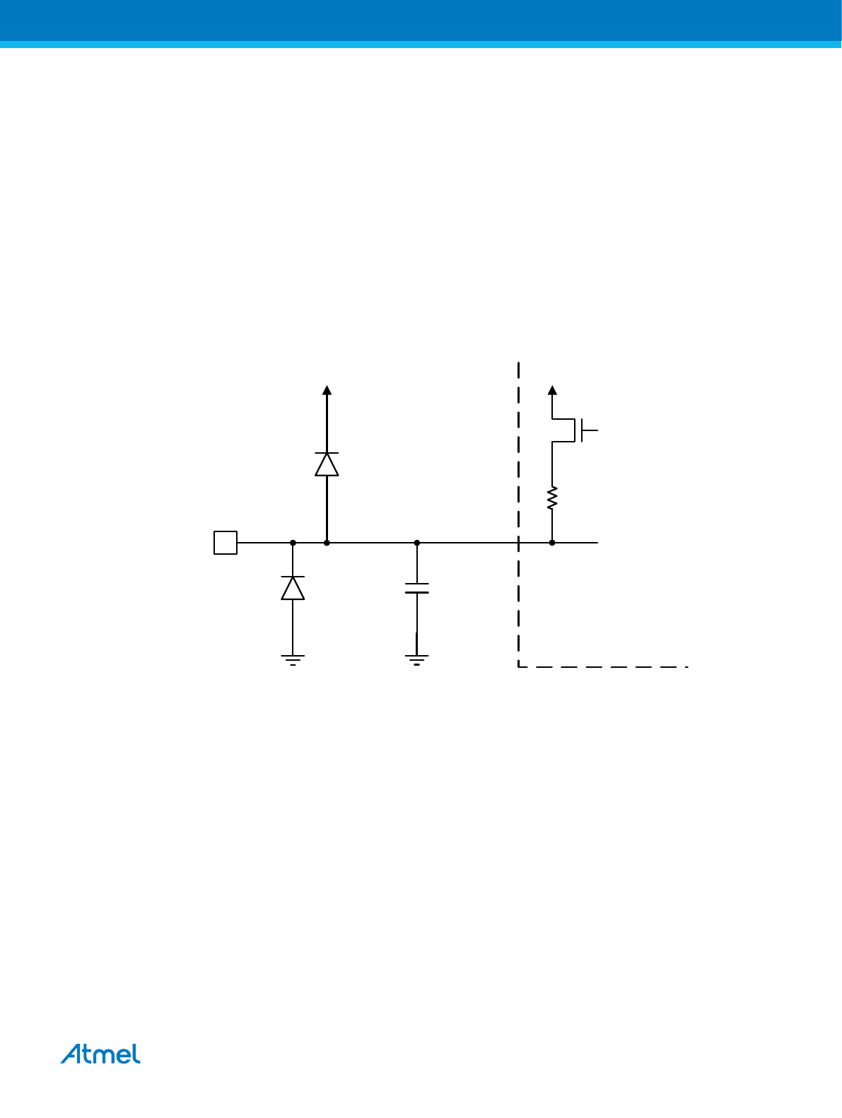
18. I/O-Ports
18.1. Overview
All AVR ports have true Read-Modify-Write functionality when used as general digital I/O ports. This
means that the direction of one port pin can be changed without unintentionally changing the direction of
any other pin with the SBI and CBI instructions. The same applies when changing drive value (if
configured as output) or enabling/disabling of pull-up resistors (if configured as input). Each output buffer
has symmetrical drive characteristics with both high sink and source capability. The pin driver is strong
enough to drive LED displays directly. All port pins have individually selectable pull-up resistors with a
supply-voltage invariant resistance. All I/O pins have protection diodes to both V
CC
and Ground as
indicated in the following figure.
Figure 18-1. I/O Pin Equivalent Schematic
C
pin
Logic
R
pu
See Figure
"General Digital I/O" for
Details
Pxn
All registers and bit references in this section are written in general form. A lower case “x” represents the
numbering letter for the port, and a lower case “n” represents the bit number. However, when using the
register or bit defines in a program, the precise form must be used. For example, PORTB3 for bit no. 3 in
Port B, here documented generally as PORTxn.
I/O memory address locations are allocated for each port, one each for the Data Register – PORTx, Data
Direction Register – DDRx, and the Port Input Pins – PINx. The Port Input Pins I/O location is read only,
while the Data Register and the Data Direction Register are read/write. However, writing '1' to a bit in the
PINx Register will result in a toggle in the corresponding bit in the Data Register. In addition, the Pull-up
Disable – PUD bit in MCUCR disables the pull-up function for all pins in all ports when set.
Using the I/O port as General Digital I/O is described in next section. Most port pins are multiplexed with
alternate functions for the peripheral features on the device. How each alternate function interferes with
the port pin is described in Alternate Port Functions section in this chapter. Refer to the individual module
sections for a full description of the alternate functions.
Enabling the alternate function of some of the port pins does not affect the use of the other pins in the
port as general digital I/O.
Atmel ATmega328/P [DATASHEET]
Atmel-42735B-ATmega328/P_Datasheet_Complete-11/2016
97
Page 98
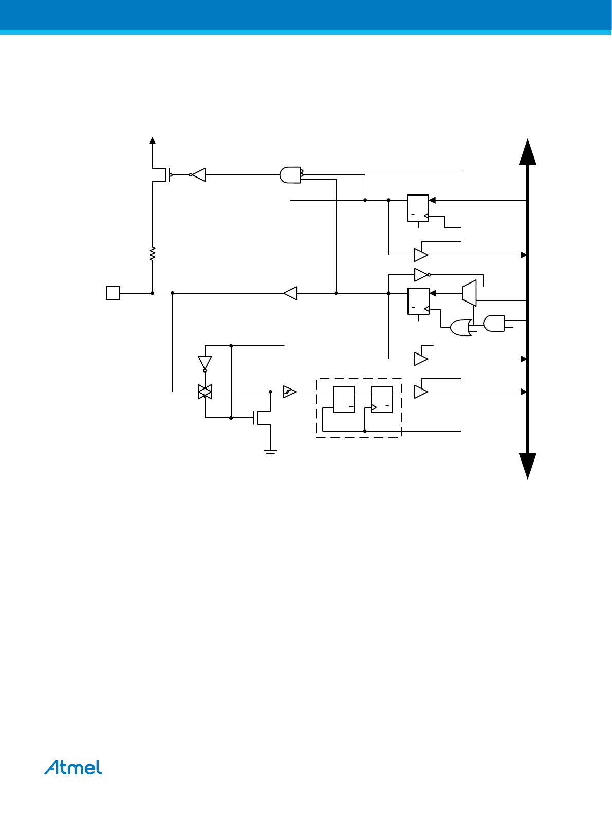
18.2. Ports as General Digital I/O
The ports are bi-directional I/O ports with optional internal pull-ups. The following figure shows the
functional description of one I/O-port pin, here generically called Pxn.
Figure 18-2. General Digital I/O
(1)
clk
RPx
RRx
RDx
WDx
PUD
SYNCHRONIZER
WDx: WRITE DDRx
WRx: WRITE PORTx
RRx: READ PORTx REGISTER
RPx: READ PORTx PIN
PUD: PULLUP DISABLE
clk
I/O
: I/O CLOCK
RDx: READ DDRx
D
L
Q
Q
RESET
RESET
Q
QD
Q
Q D
CLR
PORTxn
Q
Q D
CLR
DDxn
PINxn
DATA BUS
SLEEP
SLEEP: SLEEP CONTROL
Pxn
I/O
WPx
0
1
WRx
WPx: WRITE PINx REGISTER
Note: 1. WRx, WPx, WDx, RRx, RPx, and RDx are common to all pins within the same port. clk
I/O
,
SLEEP, and PUD are common to all ports.
18.2.1. Configuring the Pin
Each port pin consists of three register bits: DDxn, PORTxn, and PINxn. As shown in the Register
Description, the DDxn bits are accessed at the DDRx I/O address, the PORTxn bits at the PORTx I/O
address, and the PINxn bits at the PINx I/O address.
The DDxn bit in the DDRx Register selects the direction of this pin. If DDxn is written to '1', Pxn is
configured as an output pin. If DDxn is written to '0', Pxn is configured as an input pin.
If PORTxn is written to '1' when the pin is configured as an input pin, the pull-up resistor is activated. To
switch the pull-up resistor off, PORTxn has to be written to '0' or the pin has to be configured as an output
pin. The port pins are tri-stated when reset condition becomes active, even if no clocks are running.
If PORTxn is written to '1' when the pin is configured as an output pin, the port pin is driven high. If
PORTxn is written logic zero when the pin is configured as an output pin, the port pin is driven low.
Atmel ATmega328/P [DATASHEET]
Atmel-42735B-ATmega328/P_Datasheet_Complete-11/2016
98
Page 99
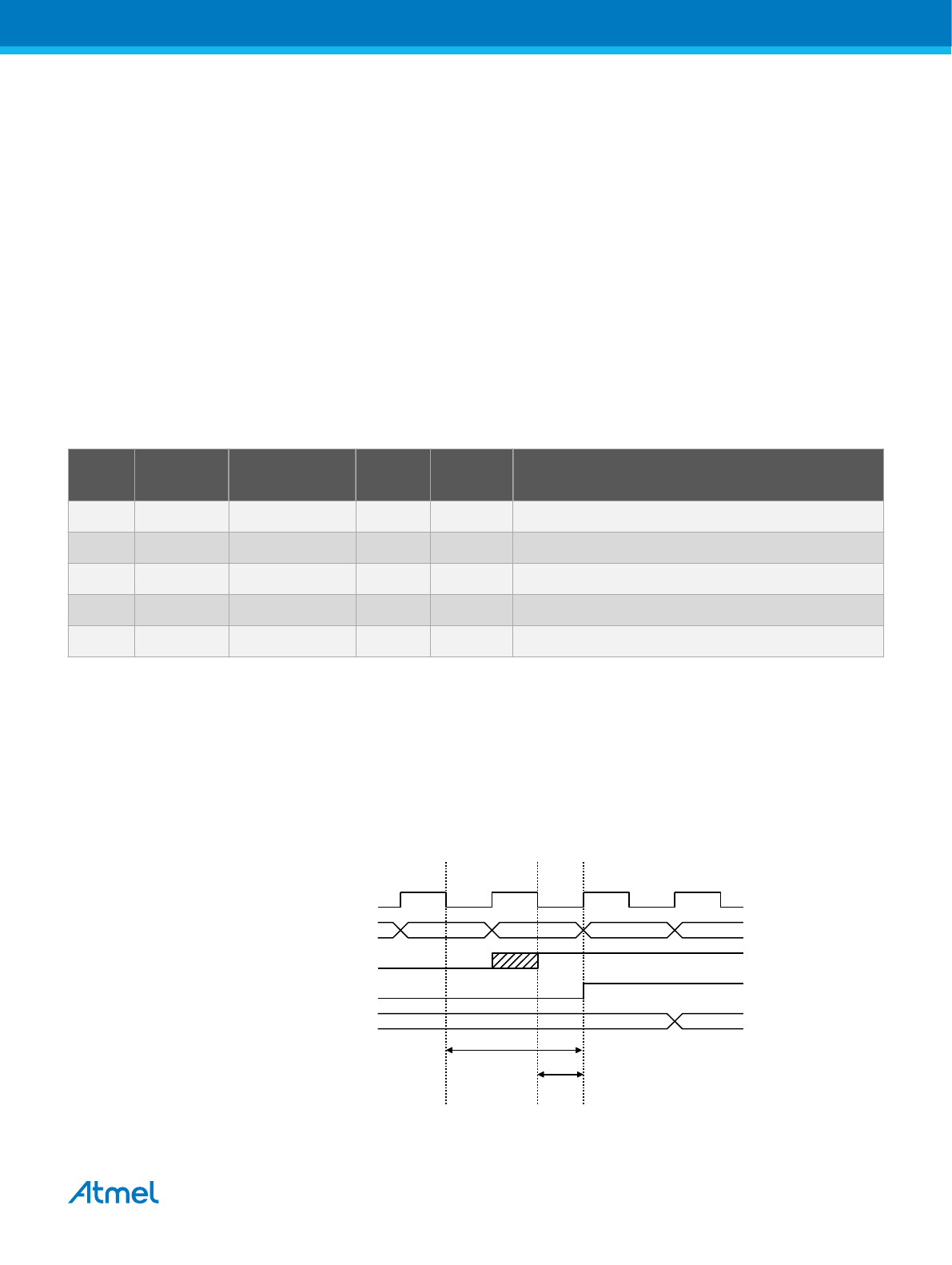
18.2.2. Toggling the Pin
Writing a '1' to PINxn toggles the value of PORTxn, independent on the value of DDRxn. The SBI
instruction can be used to toggle one single bit in a port.
18.2.3. Switching Between Input and Output
When switching between tri-state ({DDxn, PORTxn} = 0b00) and output high ({DDxn, PORTxn} = 0b11),
an intermediate state with either pull-up enabled {DDxn, PORTxn} = 0b01) or output low ({DDxn,
PORTxn} = 0b10) must occur. Normally, the pull-up enabled state is fully acceptable, as a high-
impedance environment will not notice the difference between a strong high driver and a pull-up. If this is
not the case, the PUD bit in the MCUCR Register can be set to disable all pull-ups in all ports.
Switching between input with pull-up and output low generates the same problem. The user must use
either the tri-state ({DDxn, PORTxn} = 0b00) or the output high state ({DDxn, PORTxn} = 0b11) as an
intermediate step.
The following table summarizes the control signals for the pin value.
Table 18-1. Port Pin Configurations
DDxn PORTxn PUD
(in MCUCR)
I/O Pull-up Comment
0 0 X Input No Tri-state (Hi-Z)
0 1 0 Input Yes Pxn will source current if ext. pulled low
0 1 1 Input No Tri-state (Hi-Z)
1 0 X Output No Output Low (Sink)
1 1 X Output No Output High (Source)
18.2.4. Reading the Pin Value
Independent of the setting of Data Direction bit DDxn, the port pin can be read through the PINxn
Register bit. As shown in Ports as General Digital I/O, the PINxn Register bit and the preceding latch
constitute a synchronizer. This is needed to avoid metastability if the physical pin changes value near the
edge of the internal clock, but it also introduces a delay. The following figure shows a timing diagram of
the synchronization when reading an externally applied pin value. The maximum and minimum
propagation delays are denoted t
pd,max
and t
pd,min
respectively.
Figure 18-3. Synchronization when Reading an Externally Applied Pin value
XXX in r17, PINx
0x00 0xFF
INSTRUCTIONS
SYNC LATCH
PINxn
r17
XXX
SYSTEM CLK
t
pd, max
t
pd, min
Consider the clock period starting shortly after the first falling edge of the system clock. The latch is
closed when the clock is low, and goes transparent when the clock is high, as indicated by the shaded
Atmel ATmega328/P [DATASHEET]
Atmel-42735B-ATmega328/P_Datasheet_Complete-11/2016
99
Page 100
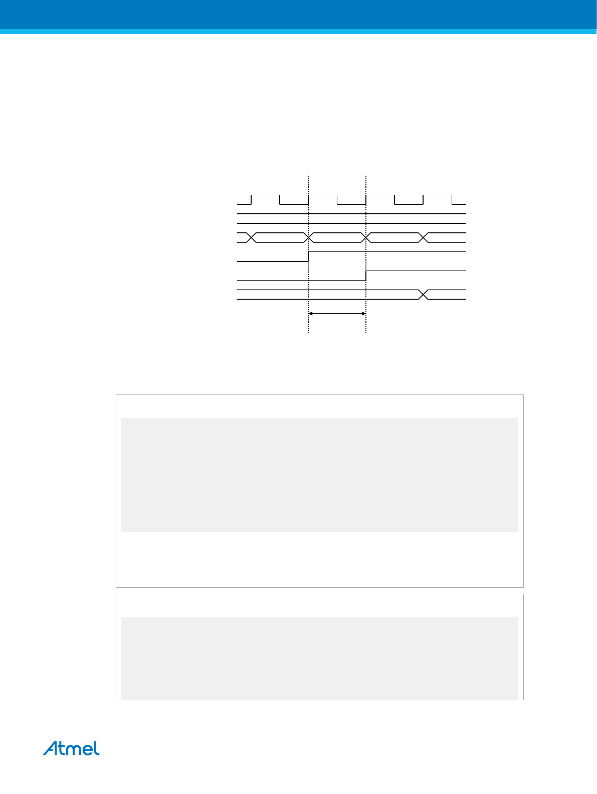
region of the “SYNC LATCH” signal. The signal value is latched when the system clock goes low. It is
clocked into the PINxn Register at the succeeding positive clock edge. As indicated by the two arrows
tpd,max and tpd,min, a single signal transition on the pin will be delayed between ½ and 1½ system clock
period depending upon the time of assertion.
When reading back a software assigned pin value, a nop instruction must be inserted as indicated in the
following figure. The out instruction sets the “SYNC LATCH” signal at the positive edge of the clock. In
this case, the delay tpd through the synchronizer is 1 system clock period.
Figure 18-4. Synchronization when Reading a Software Assigned Pin Value
out PORTx, r16 nop in r17, PINx
0xFF
0x00 0xFF
SYSTEM CLK
r16
INSTRUCTIONS
SYNC LATCH
PINxn
r17
t
pd
The following code example shows how to set port B pins 0 and 1 high, 2 and 3 low, and define the port
pins from 4 to 7 as input with pull-ups assigned to port pins 6 and 7. The resulting pin values are read
back again, but as previously discussed, a nop instruction is included to be able to read back the value
recently assigned to some of the pins.
Assembly Code Example
(1)
...
; Define pull-ups and set outputs high
; Define directions for port pins
ldi r16,(1<<PB7)|(1<<PB6)|(1<<PB1)|(1<<PB0)
ldi r17,(1<<DDB3)|(1<<DDB2)|(1<<DDB1)|(1<<DDB0)
out PORTB,r16
out DDRB,r17
; Insert nop for synchronization
nop
; Read port pins
in r16,PINB
...
Note: 1. For the assembly program, two temporary registers are used to minimize the
time from pull-ups are set on pins 0, 1, 6, and 7, until the direction bits are correctly set,
defining bit 2 and 3 as low and redefining bits 0 and 1 as strong high drivers.
C Code Example
unsigned char i;
...
/* Define pull-ups and set outputs high */
/* Define directions for port pins */
PORTB = (1<<PB7)|(1<<PB6)|(1<<PB1)|(1<<PB0);
DDRB = (1<<DDB3)|(1<<DDB2)|(1<<DDB1)|(1<<DDB0);
/* Insert nop for synchronization*/
__no_operation();
/* Read port pins */
Atmel ATmega328/P [DATASHEET]
Atmel-42735B-ATmega328/P_Datasheet_Complete-11/2016
100
 Loading...