

Page 1
6-rows 30 mA LEDs driver with boost regulator
Features
■ Boost section
– 4.5 V to 36 V input voltage range
– Internal power MOSFET
– Internal +5 V LDO for device supply
– Up to 36 V output voltage
– Constant frequency peak current-mode
control
– 250 kHz to 1 MHz adjustable switching
frequency
– External synchronization for multi-device
application
– Pulse-skip power saving mode at light load
– Programmable soft-start
– Programmable OVP protection
– Stable with ceramic output capacitors
– Thermal shutdown
■ Backlight driver section
– Six rows with 30 mA maximum current
capability (adjustable)
– Rows disable option
– Less than 500 ns minimum dimming on-
time (1 % minimum dimming duty-cycle at
20 kHz)
– ±2 % current matching between rows
– LED failure (open and short-circuit)
detection
LED7706
for LCD panels backlight
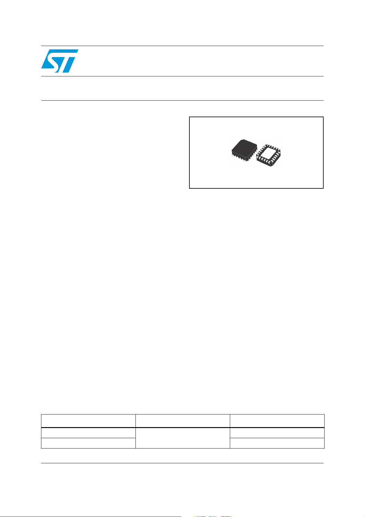
VFQFPN-24 4x4
Description
The LED7706 consists of a high efficiency
monolithic boost converter and six controlled
current generators (rows) specifically designed to
supply LEDs arrays used in the backlighting of
LCD panels. The device can manage an output
voltage up to 36 V (i.e. 10 white LEDs per row).
The generators can be externally programmed to
sink up to 30 mA and can be dimmed via a PWM
signal (1 % dimming duty-cycle at 20 kHz can be
managed). The device allows to detect and
manage the open and shorted LED faults and to
let unused rows floating. Basic protections (output
over-voltage, internal MOSFET over-current and
thermal shutdown) are provided.
Applications
■ LCD monitors and TV panels
■ PDAs panel backlight
■ GPS panel backlight
Table 1. Device summary
Order codes Package Packaging
LED7706
VFQFPN-24 4x4 (exposed pad)
LED7706TR Tape and reel
April 2009 Rev 2 1/46
Tu b e
www.st.com
46
Page 2

Contents LED7706
Contents
1 Typical application circuit . . . . . . . . . . . . . . . . . . . . . . . . . . . . . . . . . . . . 4
2 Pin settings . . . . . . . . . . . . . . . . . . . . . . . . . . . . . . . . . . . . . . . . . . . . . . . . 5
2.1 Connections . . . . . . . . . . . . . . . . . . . . . . . . . . . . . . . . . . . . . . . . . . . . . . . . 5
2.2 Pin description . . . . . . . . . . . . . . . . . . . . . . . . . . . . . . . . . . . . . . . . . . . . . . 6
3 Electrical data . . . . . . . . . . . . . . . . . . . . . . . . . . . . . . . . . . . . . . . . . . . . . . 7
3.1 Maximum rating . . . . . . . . . . . . . . . . . . . . . . . . . . . . . . . . . . . . . . . . . . . . . 7
3.2 Thermal data . . . . . . . . . . . . . . . . . . . . . . . . . . . . . . . . . . . . . . . . . . . . . . . 7
4 Electrical characteristics . . . . . . . . . . . . . . . . . . . . . . . . . . . . . . . . . . . . . 8
5 Operation description . . . . . . . . . . . . . . . . . . . . . . . . . . . . . . . . . . . . . . . 10
5.1 Boost section . . . . . . . . . . . . . . . . . . . . . . . . . . . . . . . . . . . . . . . . . . . . . . 11
5.1.1 Functional description . . . . . . . . . . . . . . . . . . . . . . . . . . . . . . . . . . . . . . 11
5.1.2 Enable function . . . . . . . . . . . . . . . . . . . . . . . . . . . . . . . . . . . . . . . . . . . 12
5.1.3 Soft-start . . . . . . . . . . . . . . . . . . . . . . . . . . . . . . . . . . . . . . . . . . . . . . . . 13
5.1.4 Overvoltage protection . . . . . . . . . . . . . . . . . . . . . . . . . . . . . . . . . . . . . . 14
5.1.5 Switching frequency selection and synchronization . . . . . . . . . . . . . . . 15
5.1.6 Slope compensation . . . . . . . . . . . . . . . . . . . . . . . . . . . . . . . . . . . . . . . 16
5.1.7 Boost current limit . . . . . . . . . . . . . . . . . . . . . . . . . . . . . . . . . . . . . . . . . 18
5.1.8 Thermal protection . . . . . . . . . . . . . . . . . . . . . . . . . . . . . . . . . . . . . . . . . 18
5.2 Backlight driver section . . . . . . . . . . . . . . . . . . . . . . . . . . . . . . . . . . . . . . 19
5.2.1 Current generators . . . . . . . . . . . . . . . . . . . . . . . . . . . . . . . . . . . . . . . . . 19
5.2.2 PWM dimming . . . . . . . . . . . . . . . . . . . . . . . . . . . . . . . . . . . . . . . . . . . . 20
5.3 Fault management . . . . . . . . . . . . . . . . . . . . . . . . . . . . . . . . . . . . . . . . . . 21
5.3.1 FAULT pin . . . . . . . . . . . . . . . . . . . . . . . . . . . . . . . . . . . . . . . . . . . . . . . 21
5.3.2 MODE pin . . . . . . . . . . . . . . . . . . . . . . . . . . . . . . . . . . . . . . . . . . . . . . . 21
5.3.3 Open LED fault . . . . . . . . . . . . . . . . . . . . . . . . . . . . . . . . . . . . . . . . . . . 22
5.3.4 Shorted LED fault . . . . . . . . . . . . . . . . . . . . . . . . . . . . . . . . . . . . . . . . . 23
2/46
Page 3

LED7706 Contents
6 Application information . . . . . . . . . . . . . . . . . . . . . . . . . . . . . . . . . . . . . 24
6.1 System stability . . . . . . . . . . . . . . . . . . . . . . . . . . . . . . . . . . . . . . . . . . . . 24
6.1.1 Loop compensation . . . . . . . . . . . . . . . . . . . . . . . . . . . . . . . . . . . . . . . . 24
6.2 Thermal considerations . . . . . . . . . . . . . . . . . . . . . . . . . . . . . . . . . . . . . . 27
6.3 Component selection . . . . . . . . . . . . . . . . . . . . . . . . . . . . . . . . . . . . . . . . 28
6.3.1 Inductor selection . . . . . . . . . . . . . . . . . . . . . . . . . . . . . . . . . . . . . . . . . . 28
6.3.2 Capacitors selection . . . . . . . . . . . . . . . . . . . . . . . . . . . . . . . . . . . . . . . 29
6.3.3 Flywheel diode selection . . . . . . . . . . . . . . . . . . . . . . . . . . . . . . . . . . . . 29
6.4 Design example . . . . . . . . . . . . . . . . . . . . . . . . . . . . . . . . . . . . . . . . . . . . 30
6.4.1 Switching frequency setting . . . . . . . . . . . . . . . . . . . . . . . . . . . . . . . . . . 30
6.4.2 Row current setting . . . . . . . . . . . . . . . . . . . . . . . . . . . . . . . . . . . . . . . . 30
6.4.3 Inductor choice . . . . . . . . . . . . . . . . . . . . . . . . . . . . . . . . . . . . . . . . . . . 30
6.4.4 Output capacitor choice . . . . . . . . . . . . . . . . . . . . . . . . . . . . . . . . . . . . . 31
6.4.5 Input capacitor choice . . . . . . . . . . . . . . . . . . . . . . . . . . . . . . . . . . . . . . 33
6.4.6 Over-voltage protection divider setting . . . . . . . . . . . . . . . . . . . . . . . . . 33
6.4.7 Compensation network . . . . . . . . . . . . . . . . . . . . . . . . . . . . . . . . . . . . . 34
6.4.8 Boost current limit . . . . . . . . . . . . . . . . . . . . . . . . . . . . . . . . . . . . . . . . . 34
6.4.9 Power dissipation estimate . . . . . . . . . . . . . . . . . . . . . . . . . . . . . . . . . . 35
6.5 Layout consideration . . . . . . . . . . . . . . . . . . . . . . . . . . . . . . . . . . . . . . . . 37
7 Electrical characteristics . . . . . . . . . . . . . . . . . . . . . . . . . . . . . . . . . . . . 41
8 Package mechanical data . . . . . . . . . . . . . . . . . . . . . . . . . . . . . . . . . . . . 43
9 Revision history . . . . . . . . . . . . . . . . . . . . . . . . . . . . . . . . . . . . . . . . . . . 45
3/46
Page 4
Typical application circuit LED7706
1 Typical application circuit
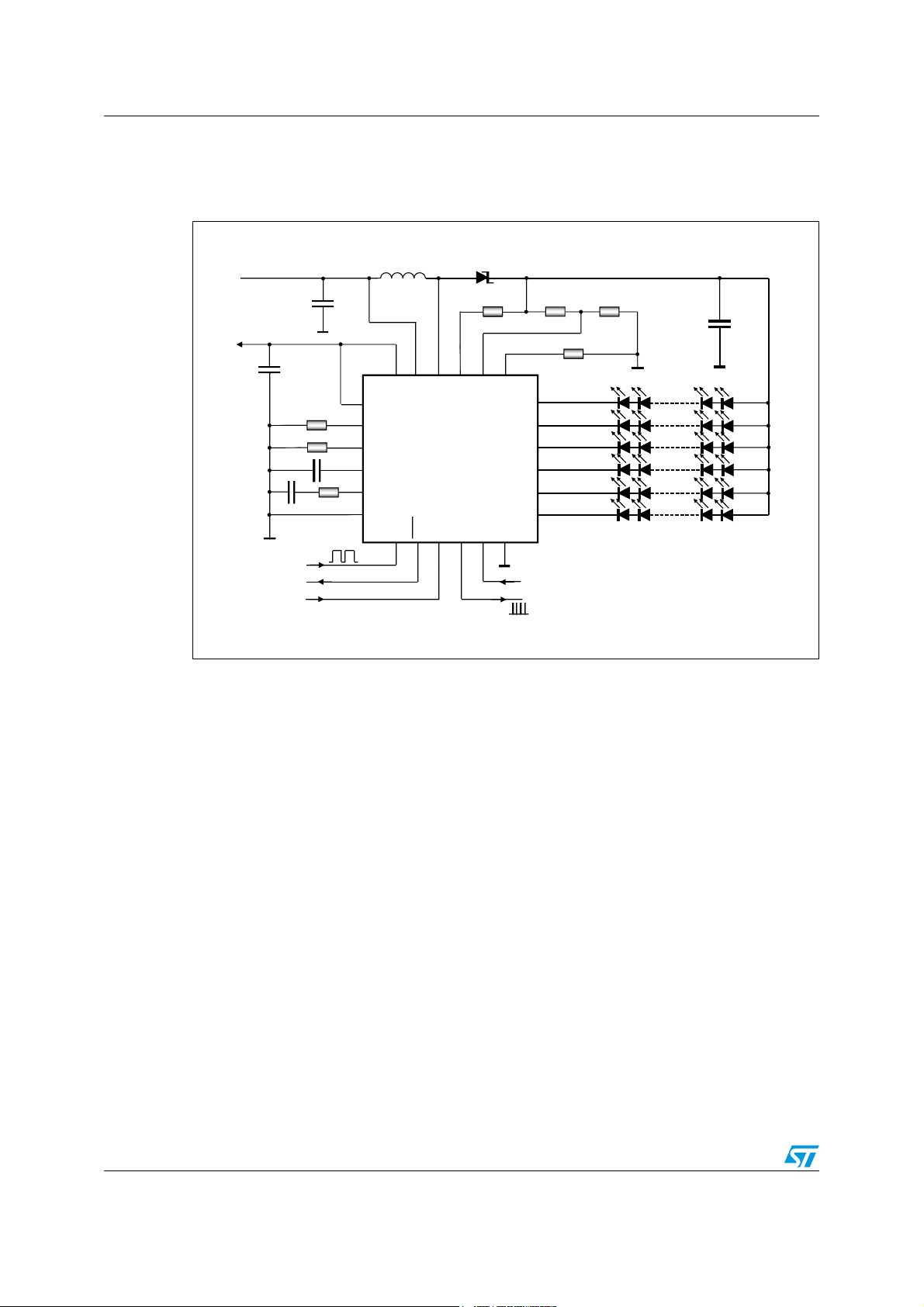
Figure 1. Application circuit
VIN
+5V
Internal MOS OCP
Rows current selection
Dimming
Fault
Enable
LDO5
BILIM
RILIM
SS
COMP
SGND
L
LX
VIN
AVCC
LED7706
FAULT
DIM
EN
Slope Compensation
OVSEL
SLOPE
MODE
SYNC
OVP selection
Switching Frequenc y selection
SWF
ROW1
ROW2
ROW3
ROW4
ROW5
ROW6
PGND
Faults Management Selection
Sync Output
MLCC
Up to 10 WLEDs per row
OUT
V
AM00594v1
4/46
Page 5
LED7706 Pin settings
2 Pin settings
2.1 Connections
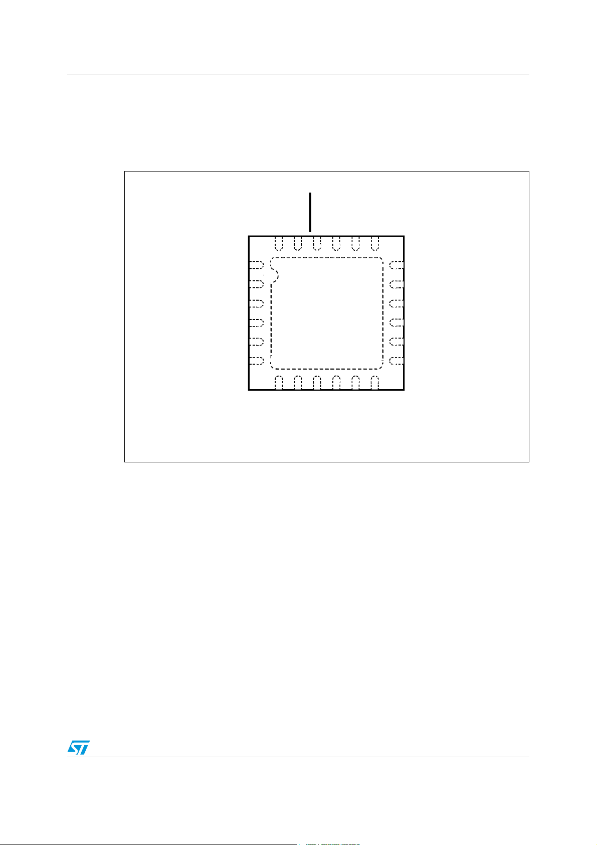
Figure 2. Pin connection (through top view)
COMP
RILIM
BILIM
FSW
MODE
AVCC
SYNC
SS
24
1
EN
DIM
FAULT
LX
19
18
OVSEL
PGND
LED7706
ROW6
ROW5
ROW4
ROW3
6
7
13
12
VIN
LDO5
SGND
SLOPE
ROW2
ROW1
AM00595v1
5/46
Page 6
Pin settings LED7706
2.2 Pin description
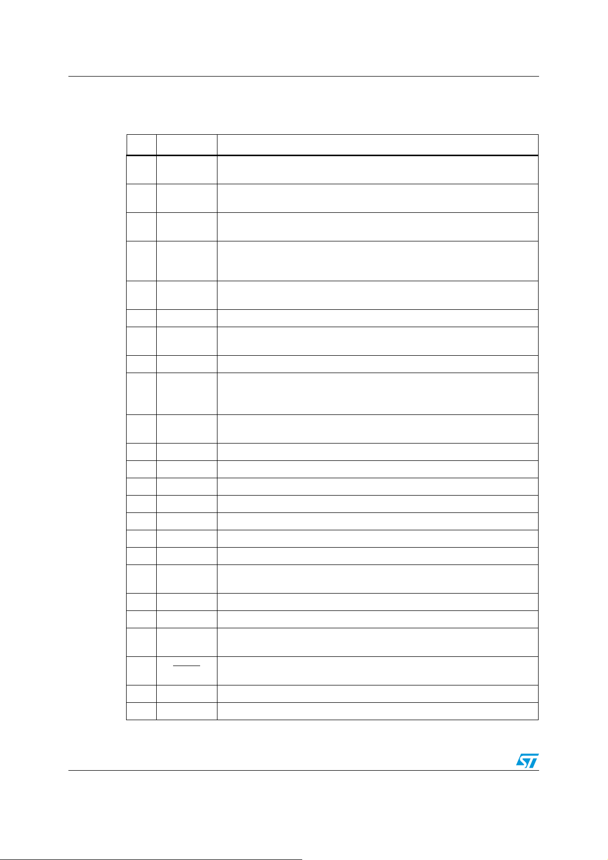
Table 2. Pin functions
N° Pin Function
1COMP
2RILIM
3 BILIM
4FSW
5MODE
6 AVCC + 5 V analog supply. Connect to LDO5 through a simple RC filter.
7LDO5
8 VIN Input voltage. Connect to the main supply rail.
9SLOPE
10 SGND
11 ROW1 Row driver output #1.
Error amplifier output. A simple RC series between this pin and ground is
needed to compensate the loop of the boost regulator.
Output generators current limit setting. The output current of the rows can be
programmed connecting a resistor to SGND.
Boost converter current limit setting. The internal MOSFET current limit can
be programmed connecting a resistor to SGND.
Switching frequency selection and external sync input. A resistor to SGND is
used to set the desired switching frequency. The pin can also be used as
external synchronization input. See
Current generators fault management selector. It allows to detect and manage
LEDs failures. See
+ 5 V LDO output and power section supply. Bypass to SGND with a
1 μF ceramic capacitor.
Slope compensation setting. A resistor between the output of the boost
converter and this pin is needed to avoid sub-harmonic instability.
Refer to
Signal ground. Supply return for the analog circuitry and the current
generators.
Section 6.1 on page 24 for details.
Section 5.3.2 on page 21 for details.
Section 5.1.5 on page 15 for details.
12 ROW2 Row driver output #2.
13 ROW3 Row driver output #3.
14 ROW4 Row driver output #4.
15 ROW5 Row driver output #5.
16 ROW6 Row driver output #6.
17 PGND Power ground. Source of the internal Power MOSFET.
18 OVSEL
19 LX Switching node. Drain of the internal Power MOSFET.
20 DIM Dimming input. Used to externally set the brightness by using a PWM signal.
21 EN
22 FAULT
23 SYNC Synchronization output. Used as external synchronization output.
24 SS Soft-start. Connect a capacitor to SGND to set the desired soft-start duration.
6/46
Over-voltage selection. Used to set the desired OV threshold by an external
divider. See
Enable input. When low, the device is turned off. If tied high or left open, the
device is turned on and a soft-start sequence takes place.
Fault signal output. Open drain output. The pin goes low when a fault condition
is detected (see Section 5.3.1 on page 21 for details).
Section 5.1.4 on page 14 for details.
Page 7
LED7706 Electrical data
3 Electrical data
3.1 Maximum rating
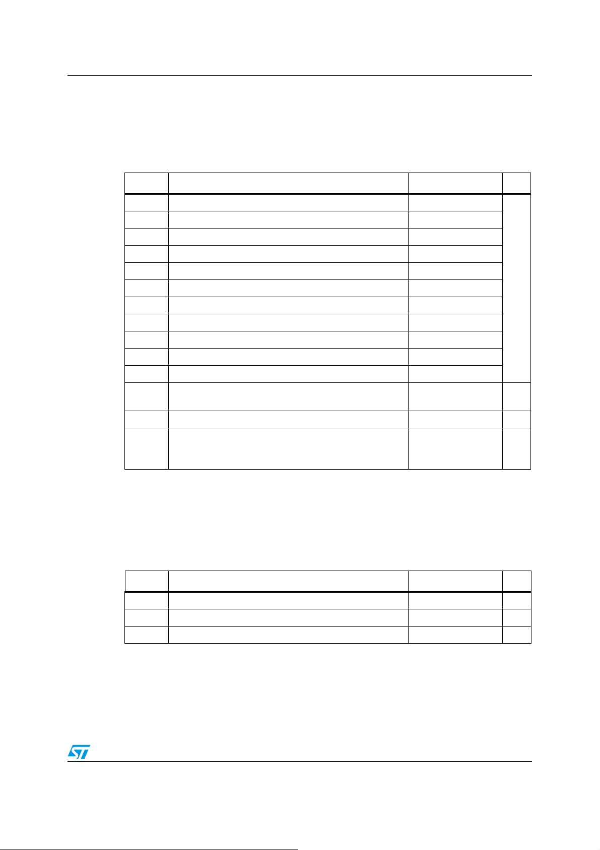
Table 3. Absolute maximum ratings
(1)
Symbol Parameter Value Unit
V
AVC C
V
LDO5
AVCC to SGND -0.3 to 6
LDO5 to SGND -0.3 to 6
PGND to SGND -0.3 to 0.3
V
V
VIN to PGND -0.3 to 40
IN
LX to SGND -0.3 to 40
LX
LX to PGND -0.3 to 40
RILIM, BILIM, SYNC, OVSEL, SS to SGND -0.3 to V
AVC C
+ 0.3
EN, DIM, SW, MODE, FAULT to SGND -0.3 to 6
ROWx to PGND/ SGND -0.3 to 40
SLOPE to VIN V
- 0.3 to VIN + 6
IN
SLOPE to SGND -0.3 to 40
Internal switch maximum RMS current
(flowing through LX node)
P
Power dissipation @ TA = 25 °C 2.3
TOT
2.0 A
(2)
Maximum withstanding voltage range test condition:
CDF-AEC-Q100-002- “human body model” acceptance
±1000 V
criteria: “normal performance”
1. Stresses beyond those listed under “absolute maximum ratings” may cause permanent damage to the
device. Exposure to absolute maximum rated conditions for extended periods may affect device reliability.
2. Power dissipation referred to the device mounted on the demonstration board described in section 5.5
V
W
3.2 Thermal data
Table 4. Thermal data
Symbol Parameter Value Unit
R
T
Thermal resistance junction to ambient 42 °C/W
thJA
Storage temperature range -50 to 150 °C
STG
Junction operating temperature range -40 to 150 °C
T
J
7/46
Page 8
Electrical characteristics LED7706
4 Electrical characteristics
VIN = 12 V; TJ = 25 °C and LDO5 connected to AVCC if not otherwise specified
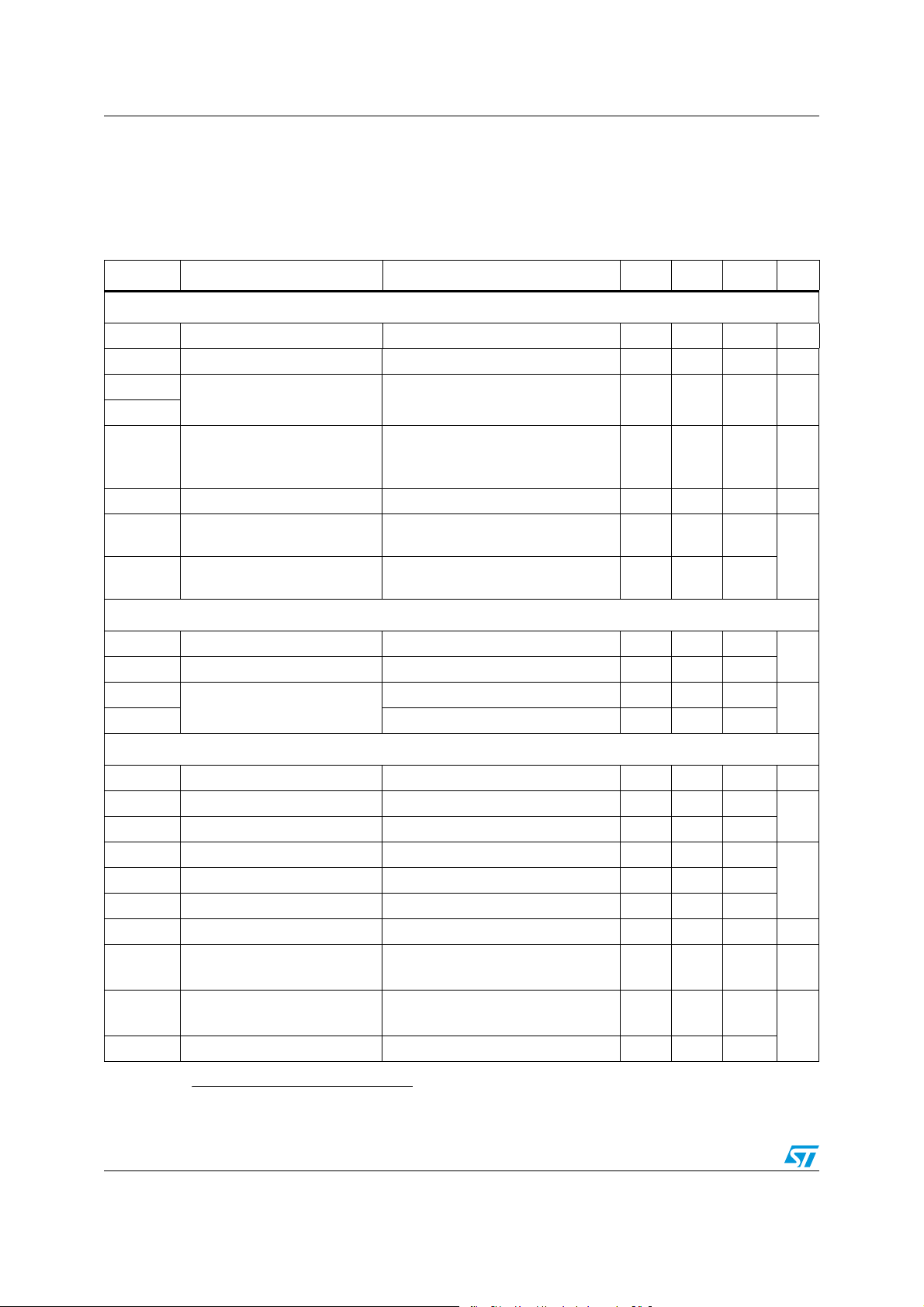
Table 5. Electrical characteristics
(a)
Symbol Parameter Test condition Min. Typ. Max. Unit
Supply section
V
V
V
I
V
BST
LDO5
AVC C
IN,Q
Input voltage range 4.5 36 V
IN
Boost section output voltage 36
LDO output and IC supply
voltage
Operating quiescent current
EN High
= 0 mA
I
LDO5
= 51 kΩ, R
R
RILIM
R
SLOPE
= 680 kΩ
BILIM
4.4 5 5.5 V
= 220 kΩ,
1mA
DIM tied to SGND.
I
IN,SHDN
V
UVLO,ON
V
UVLO,OFF
Operating current in shutdown EN low 20 30 μA
LDO5 under voltage lock out
upper threshold
LDO5 under voltage lock out
lower threshold
3.3 3.6
3.8 4.0
LDO linear regulator
Line regulation 6 V
LDO dropout voltage V
LDO maximum output current
V
V
IN
LDO5
LDO5
≤ 36 V, I
IN
= 4.3 V, I
> V
UVLO,ON
< V
UVLO,OFF
LDO5
= 30 mA 30
LDO5
= 10 mA 80 120
25 40 60
20 30
≤ V
Boost section
V
mV
mA
t
ON,min
f
SW
Minimum switching on-time 200 ns
Default switching frequency FSW connected to AVCC 570 660 750
Minimum FSW sync frequency 210
FSW sync input threshold 240
FSW sync input hysteresis 20
FSW sync min. ON time 270 ns
SYNC output Duty-Cycle
SYNC output high level I
SYNC output low level I
a. Specification referred to TJ from 0 °C to +85 °C. Specification over the 0 to +85 °C TJ range are assured by
design, characterization and statistical correlation.
FSW connected to AVCC
(Internal oscillator selected)
= 10 μA
SYNC
= -10 μA 20
SYNC
8/46
V
AVC C
-20V
kHz
mVFSW sync low level 350
34 40 %
mV
Page 9
LED7706 Electrical characteristics
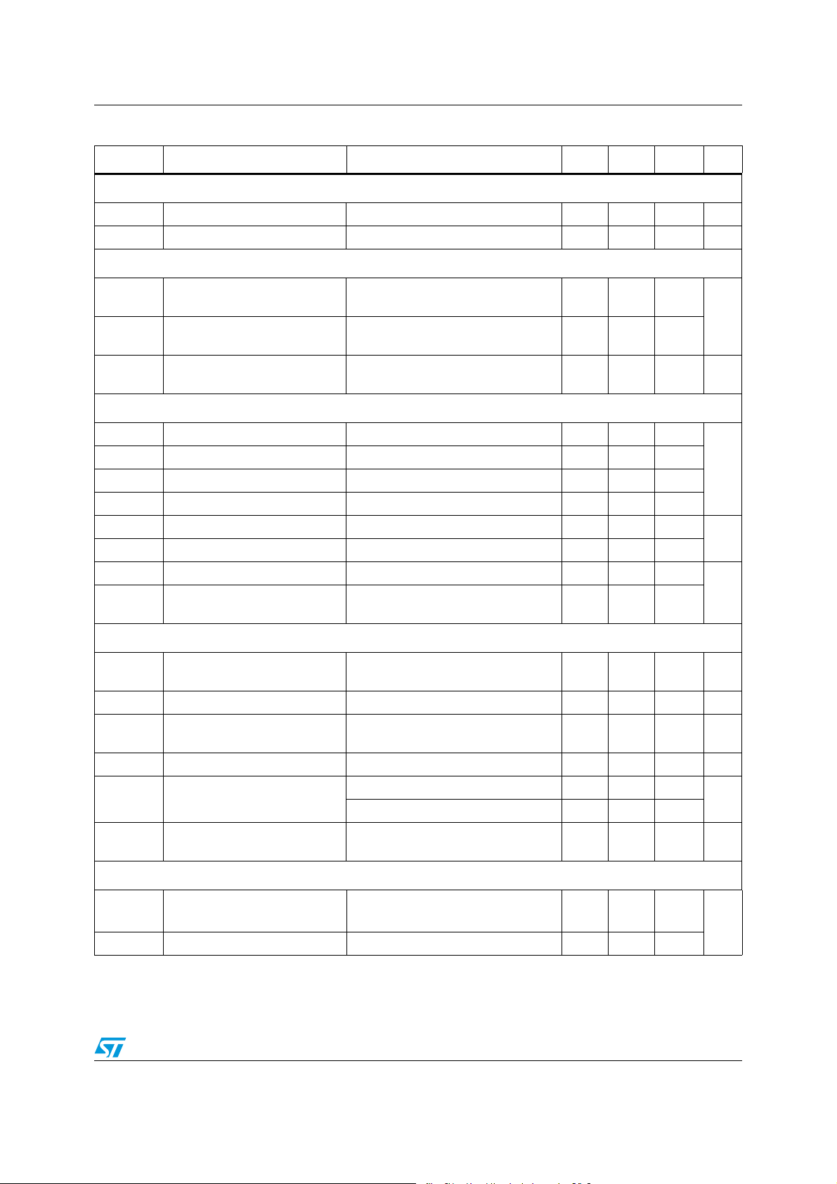
Table 5. Electrical characteristics (continued)
Symbol Parameter Test condition Min. Typ. Max. Unit
Power switch
5
V
R
K
DSon
LX current coefficient R
B
Internal MOSFET on-resistance
OC and OV protections
= 600 kΩ 5·1056·1057·10
BILIM
280 500 mΩ
V
TH,OVP
V
TH,FRD
ΔV
OVP,FRD
Over voltage protection
reference threshold (OVSEL)
Floating channel detection
threshold
Voltage gap between OVP and
FRD thresholds
Soft-start and power management
EN, Turn-on threshold 1.6
EN, Turn-off threshold 0.8
DIM, high level threshold 1.3
DIM, low level threshold 0.8
EN, pull-up current 2.5
SS, charge current 4 5 6
SS, end-of-startup threshold 2.0 2.4 2.8
SS, reduced switching
frequency release threshold
Current generators section
T
DIM-
ON,min
K
ΔK
V
IFB
V
rowx,
FAULT
V
FAU LT,
LOW
Minimum dimming on-time 500 ns
Current generators gain 987 V
R
Current generators gain
(1)
R
accuracy
Feedback regulation voltage 400 mV
Shorted LED fault detection
threshold
FAULT pin low-level voltage I
Thermal shutdown
1.190 1.234 1.280
1.100 1.145 1.190
90 mV
0.8
MODE tied to SGND 3.4
MODE connected to AVCC 6.0
FAULT,SINK
= 4 mA 200 350 mV
V
V
μA
V
±2.0 %
V
1. I
T
SHDN
ROW
Thermal shutdown
turn-off temperature
Thermal shutdown hysteresis 30
= KR / R
, ΔI
RILIM
ROW/IROW ≈ ΔKR/KR
+ ΔR
RILIM/RRILIM
9/46
150
°C
Page 10
Operation description LED7706
5 Operation description
The device can be divided into two sections: the boost section and the backlight driver
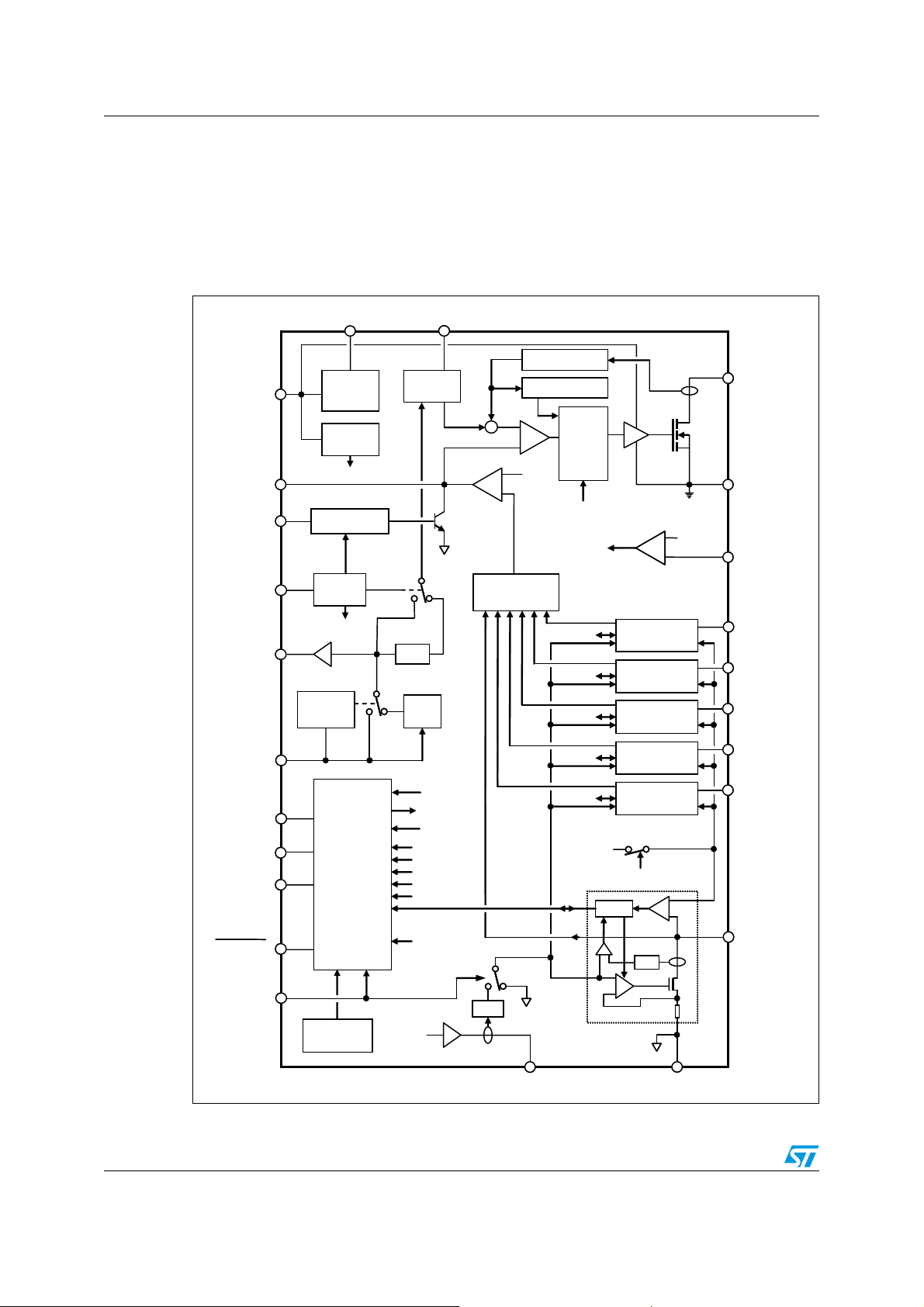
section. These sections are described in the next paragraphs. Figure 3 provides an
overview of the internal blocks of the device.
Figure 3. Simplified block diagram
VIN
LDO5
LDO5
COMP
COMP
BILIM
BILIM
SS
SS
SYNC
SYNC
FSW
FSW
AVCC
AVCC
EN
EN
MODE
MODE
FAULT
FAULT
DIM
DIM
VIN
+5V
+5V
LDO
LDO
UVLO
UVLO
Detector
Detector
UVLO
UVLO
Current Limit
Current Limit
Soft Start
Soft Start
Prot_EN
Prot_EN
Ext Sync
Ext Sync
Detector
Detector
CONTROL
CONTROL
LOGIC
LOGIC
Thermal
Thermal
Shutdown
Shutdown
SLOPE
SLOPE
Ramp
Ramp
Generator
Generator
÷2
÷2
OSC
OSC
Prot_EN
Prot_EN
Boost_EN
Boost_EN
UVLO
UVLO
CTRL6
CTRL6
CTRL5
CTRL5
CTRL4
CTRL4
CTRL3
CTRL3
CTRL2
CTRL2
OVP
OVP
1.2V
1.2V
+
+
+
+
+
+
g
m
g
m
_
_
Min Voltage
Min Voltage
Selector
Selector
CTRL1
CTRL1
ROW1
ROW1
V
V
I to V
I to V
Current Sense
Current Sense
ZCD
ZCD
+
+
Boost
Boost
Control
Control
_
_
Logic
Logic
0.7V
0.7V
Boost_EN
Boost_EN
CTRL6
CTRL6
CTRL5
CTRL5
CTRL4
CTRL4
CTRL3
CTRL3
CTRL2
CTRL2
OVP
OVP
V
ROW6
V
ROW6
V
ROW5
V
ROW5
V
ROW4
V
ROW4
V
ROW3
V
ROW3
V
ROW2
V
ROW2
4V
4V
LOGIC
LOGIC
Current
Current
Generator 1
Generator 1
Current
Current
Generator 6
Generator 6
Current
Current
Generator 5
Generator 5
Current
Current
Generator 4
Generator 4
Current
Current
Generator 3
Generator 3
Current
Current
Generator 2
Generator 2
MODE
MODE
I to V
I to V
+
+
_
_
_
_
+
+_+
V
V
TH,FLT
TH,FLT
1.172V
1.172V
LX
LX
PGND
PGND
OVSEL
OVSEL
ROW6
ROW6
ROW5
ROW5
ROW4
ROW4
ROW3
ROW3
ROW2
ROW2
ROW1
ROW1
10/46
RILIM
RILIM
SGND
SGND
AM00596v1
Page 11
LED7706 Operation description
5.1 Boost section
5.1.1 Functional description
The LED7706 is a monolithic LEDs driver for the backlight of LCD panels and it consists of a
boost converter and six PWM-dimmable current generators.
The boost section is based on a constant switching frequency, peak current-mode
architecture. The boost output voltage is controlled such that the lowest row's voltage,
referred to SGND, is equal to an internal reference voltage (400 mV typ. see Figure 5). The
input voltage range is from 4.5 V up to 36 V. In addition, the LED7706 has an internal LDO
that supplies the internal circuitry of the device and is capable to deliver up to 40 mA. The
input of the LDO is the VIN pin.
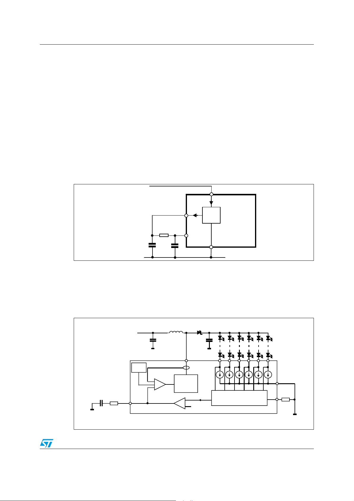
The LDO5 pin is the LDO output and the supply for the power MOSFET driver at the same
time. The AVCC pin is the supply for the analog circuitry and should be connected to the
LDO output through a simple RC filter in order to improve the noise rejection.
Figure 4. AVCC filtering
VIN
VIN
LDO5
CLDO5
CLDO5
1uF
1uF
Rfilt
Rfilt
4R7
4R7
C
C
AVCC
AVCC
100nF
100nF
LDO5
AVCC
AVCC
LDO
LDO
SGND
SGND
LED7706
LED7706
AM00597v1
Two loops are involved in regulating the current sunk by the generators.
The main loop is related to the boost regulator and uses a constant frequency peak currentmode architecture to regulate the power rail that supplies the LEDs (Figure 5), while an
internal current loop regulates the same current (flowing through the LEDs) at each row
according to the set value (RILIM pin).
Figure 5. Main loop and current loop diagram
V
IN
LX
Slope
PWM
ROWx
SGND
COMP
RILIM
E/A
Error amplifier
Minimum voltage drop
selector
0.4V
11/46
AM00598v1
Page 12
Operation description LED7706
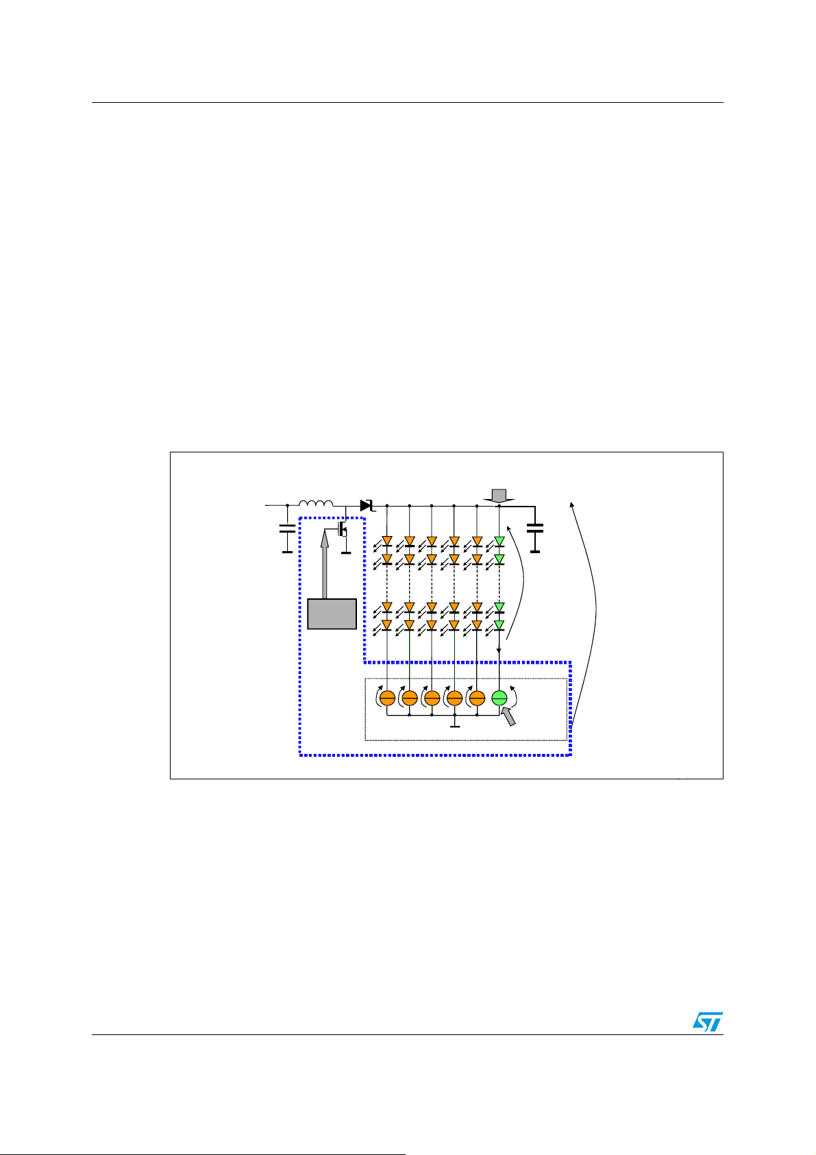
A dedicated circuit automatically selects the lowest voltage drop among all the rows and
provides this voltage to the main loop that, in turn, regulates the output voltage. In fact, once
the reference generator has been detected, the error amplifier compares its voltage drop to
the internal reference voltage and varies the COMP output. The voltage at the COMP pin
determines the inductor peak current at each switching cycle. The output voltage of the
boost regulator is thus determined by the total forward voltage of the LEDs strings (see
Figure 6):
Equation 1
m
N
OUT
ROWS
=
1i
LEDS
Σ
=
mV400)V(maxV
+=
j,F
1j
where the first term represents the highest total forward voltage drop over N active rows and
the second is the voltage drop across the leading generator (400 mV typ.).
The device continues to monitor the voltage drop across all the rows and automatically
switches to the current generator having the lowest voltage drop.
Figure 6. Calculation of the output voltage of the boost regulator
Row with the highest voltage
V
IN
drop across LEDs
5.1.2 Enable function
The LED7706 is enabled by the EN pin. This pin is active high and, when forced to SGND,
the device is turned off. This pin is connected to a permanently active 2.5 μA current source;
when sudden device turn-on at power-up is required, this pin must be left floating or
connected to a delay capacitor. When turned off, the LED7706 quickly discharges the
soft-start capacitor and turns off the power MOSFET, the current generators and the LDO.
The power consumption is thus reduced to 20 μA only.
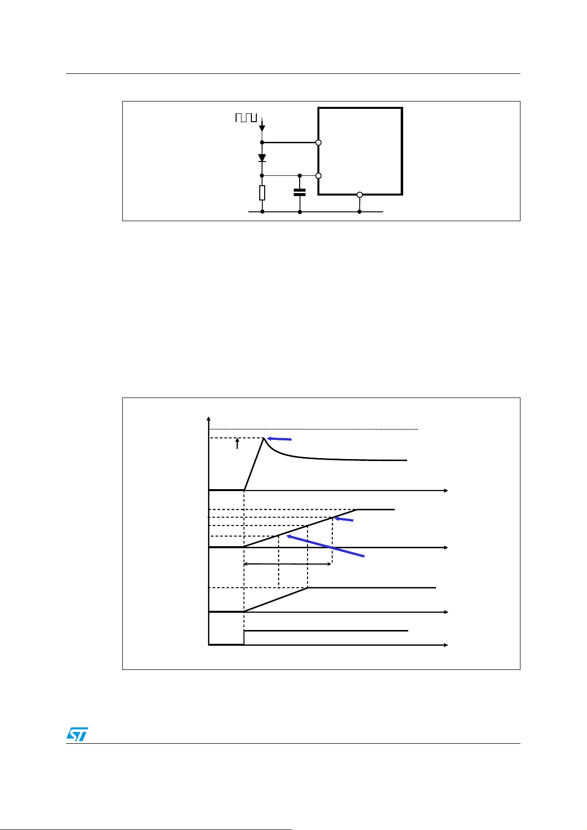
In applications where the dimming signal is used to turn on and off the device, the EN pin
can be connected to the DIM pin as shown in Figure 7.
Boost
controller
Current
generators
section
I
LED
400 mV
generator
max
Σ
Leading
V
F
V
BOOST
AM00599v1
12/46
Page 13
LED7706 Operation description
Figure 7. Enable pin driven by dimming signal
DIM
DIM
BAS69
BAS69
EN
220kΩ
220kΩ
100nF
100nF
EN
LED7706
LED7706
SGND
SGND
AM00600v1
5.1.3 Soft-start
The soft-start function is required to perform a correct start-up of the system, controlling the
inrush current required to charge the output capacitor and to avoid output voltage overshoot.
The soft-start duration is set connecting an external capacitor between the SS pin and
ground. This capacitor is charged with a 5 μA (typ.) constant current, forcing the voltage on
the SS pin to ramp up. When this voltage increases from zero to nearly 1.2 V, the current
limit of the power MOSFET is proportionally released from zero to its final value. However,
because of the limited minimum on-time of the switching section, the inductor might saturate
due to current runaway. To solve this problem the switching frequency is reduced to one half
of the nominal value at the beginning of the soft-start phase. The nominal switching
frequency is restored after the SS pin voltage has crossed 0.8 V.
Figure 8. Soft-start sequence waveforms in case of floating rows
OVP
OVP
Floating ROWs detection
Floating ROWs detection
95% of
95% of
OVP
AVCC
AVCC
2.4V
2.4V
1.2V
1.2V
0.8V
0.8V
100%
100%
OVP
t
ss
t
ss
Current limit
Current limit
Output voltage
Output voltage
SS pin voltage
SS pin voltage
Protections turn active
Protections turn active
Nominal switching
Nominal switching
frequency release
frequency release
EN pin voltage
EN pin voltage
t
t
AM00601v1
During the soft-start phase the floating rows detection is also performed. In presence of one
or more floating rows, the voltage across the involved current generator drops to zero. This
voltage becomes the inverting input of the error amplifier through the minimum voltage drop
13/46
Page 14

Operation description LED7706
selector (see Figure 5). As a consequence the error amplifier is unbalanced and the loop
reacts by increasing the output voltage. When it reaches the floating row detection (FRD)
threshold (95% of the OVP threshold), the floating rows are managed according to
Section 5.3 on page 21). After the SS voltage reaches a 2.4 V threshold, the start-up
(see
finishes and all the protections turn active. The soft-start capacitor C
can be calculated
SS
Ta bl e 6
according to equation 2.
Equation 2
⋅
tI
≅
C
SS
SSSS
4.2
Where I
= 5 µA and tSS is the desired soft-start duration.
SS
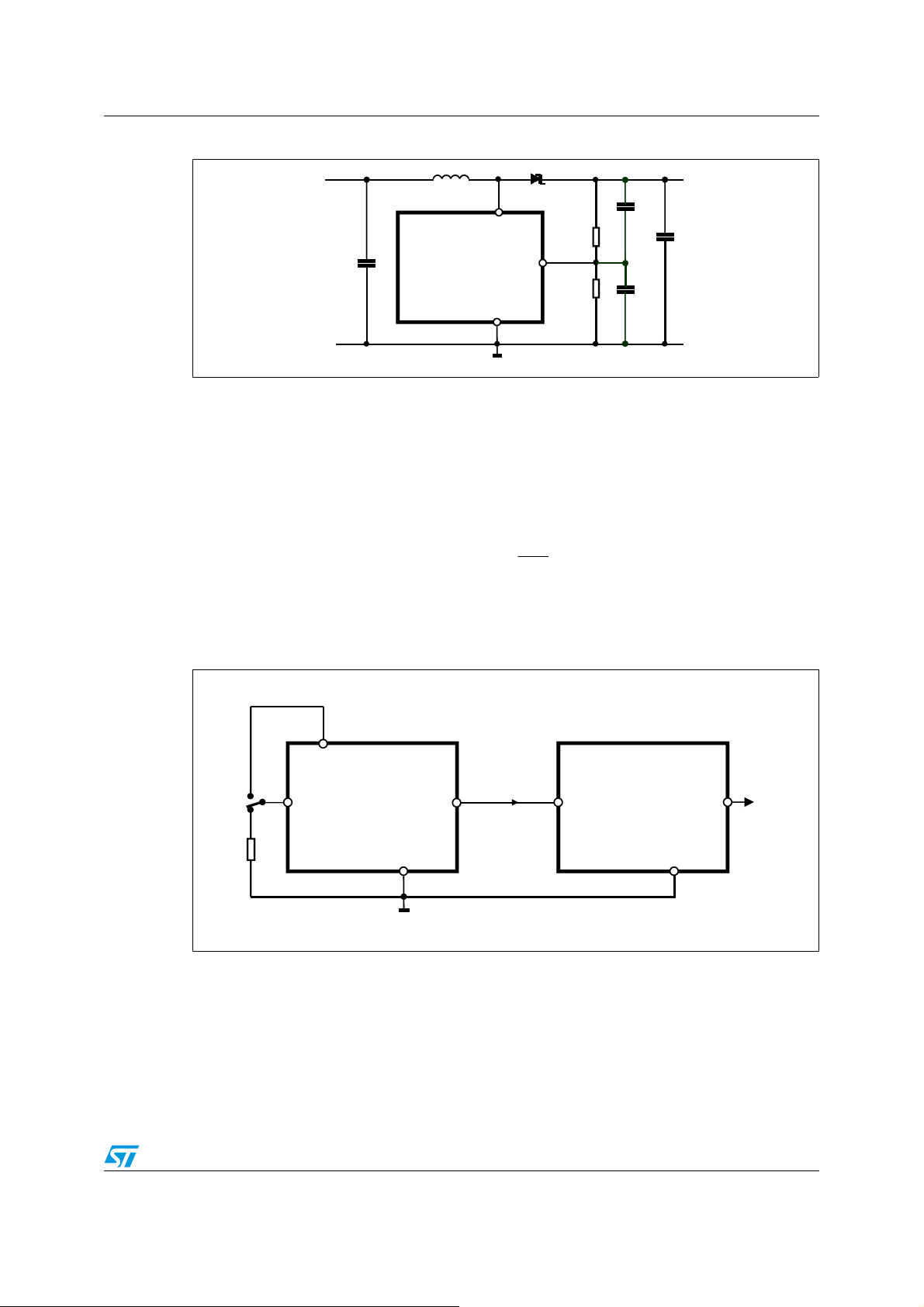
5.1.4 Overvoltage protection
An adjustable over-voltage protection is available. It can be set feeding the OVSEL pin with a
partition of the output voltage. The voltage of the central tap of the divider is thus compared
to a fixed 1.234 V threshold. When the voltage on the OVSEL pin exceeds the OV threshold,
the FAULT pin is tied low and the device is turned off; this condition is latched and the
LED7706 is restarted
occurs when the LDO output falls below the lower UVLO threshold and subsequently
crosses the upper UVLO threshold during the rising phase of the input voltage). Normally,
the value of the high-side resistors of the divider must be chosen as high as possible (but
lower than 1 M
(during the off phase of the dimming cycle). The R2/R1 ratio is calculated to trigger the OVP
circuitry as soon as the output voltage is 2 V higher than the maximum value for a given LED
string (see equation 3). Two additional filtering capacitors, C
improve noise rejection at the OVSEL pin, as shown in
in the 100 pF-330 pF range, while the C
Equation 3
by toggling the EN pin or by performing a Power-On Reset (the POR
Ω) to reduce the output capacitor discharge when the boost converter is off
Figure 9. The typical value for C10 is
13 value is given by equation 4.
RR
⋅=
12
OVP,OUT
V234.1
−+
10 and C13, may be required to
)V234.1V2V(
Equation 4
14/46
R
2
C2C ⋅=
1013
R
1
Page 15
LED7706 Operation description
Figure 9. OVP threshold setting
V
IN
LX
OVSEL
LED7706
SGND
R
R
V
OUT
C
13
C
1
2
OUT
C
10
AM00602v1
5.1.5 Switching frequency selection and synchronization
The switching frequency of the boost converter can be set in the 250 kHz-1 MHz range by
connecting the FSW pin to ground through a resistor. Calculation of the setting resistor is
made using equation 5 and should not exceed the 100 kΩ-400 kΩ range.
Equation 5
F
SW
=
R
FSW
5.2
In addition, when the FSW pin is tied to AVCC, the LED7706 uses a default 660 kHz fixed
switching frequency, allowing to save a resistor in minimum component-count applications.
Figure 10. Multiple device synchronization
MASTER
AVCC
FSW SYNC
SYNC
FSW
LED7706
FSW
R
SGND
SLAVE
Sync Out
SYNC
LED7706
SGND
AM00603v1
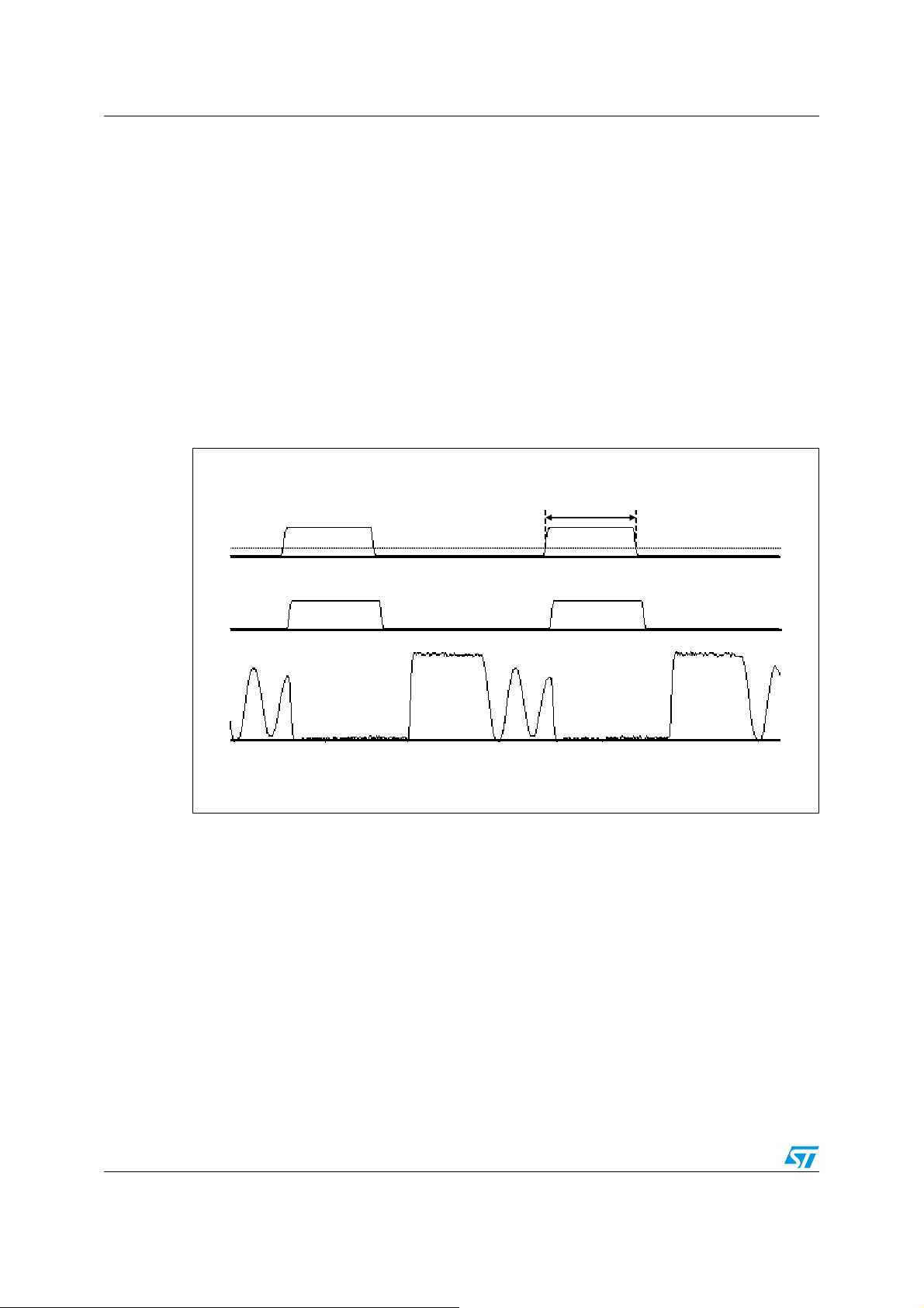
The FSW pin can also be used as synchronization input, allowing the LED7706 to operate
both as master or slave device. If a clock signal with a 210 kHz minimum frequency is
applied to this pin, the device locks synchronized. The signal provided to the FSW pin must
cross the 270 mV threshold in order to be recognized. The minimum pulse width which
allows the synchronizing pulses to be detected is 270 ns. An Internal time-out allows
synchronization as long as the external clock frequency is greater than 210 kHz.
15/46
Page 16
Operation description LED7706
Keeping the FSW pin voltage lower than 270 mV for more than 4.8 µs results in a stop of the
device switching activity. Normal operation is resumed as soon as FSW rises above the
mentioned threshold and the soft-start sequence is repeated.
The SYNC pin is a synchronization output and provides a 35 % (typ.) duty-cycle clock when
the LED7706 is used as master or a replica of the FSW pin when used as slave. It is used to
connect multiple devices in a daisy-chain configuration or to synchronize other switching
converters running in the system with the LED7706 (master operation). When an external
synchronization clock is applied to the FSW pin, the internal oscillator is over-driven: each
switching cycle begins at the rising edge of the clock, while the slope compensation
(
Figure 11) ramp starts at the falling edge of the same signal. Thus, to prevent sub-
harmonic instability (see
Section 5.1.6), the external synchronization clock is required to
have a 40 % maximum duty-cycle when the boost converter is working in continuousconduction mode (CCM) in order to assure that the slope compensation is effective (starts
with duty-cycle lower than 40%)
Figure 11. External sync waveforms
FSW pin voltage (ext. sync)
Slave SYNC pin voltage
Slave LX pin voltage
5.1.6 Slope compensation
The constant frequency, peak current-mode topology has the advantage of very easy loop
compensation with output ceramic caps (reduced cost and size of the application) and fast
transient response. In addition, the intrinsic peak-current measurement simplifies the
current limit protection, avoiding undesired saturation of the inductor.
On the other side, this topology has a drawback: there is an inherent open loop instability
when operating with a duty-ratio greater than 0.5. This phenomenon is known as “SubHarmonic Instability” and can be avoided by adding an external ramp to the one coming
from the sensed current. This compensating technique, based on the additional ramp, is
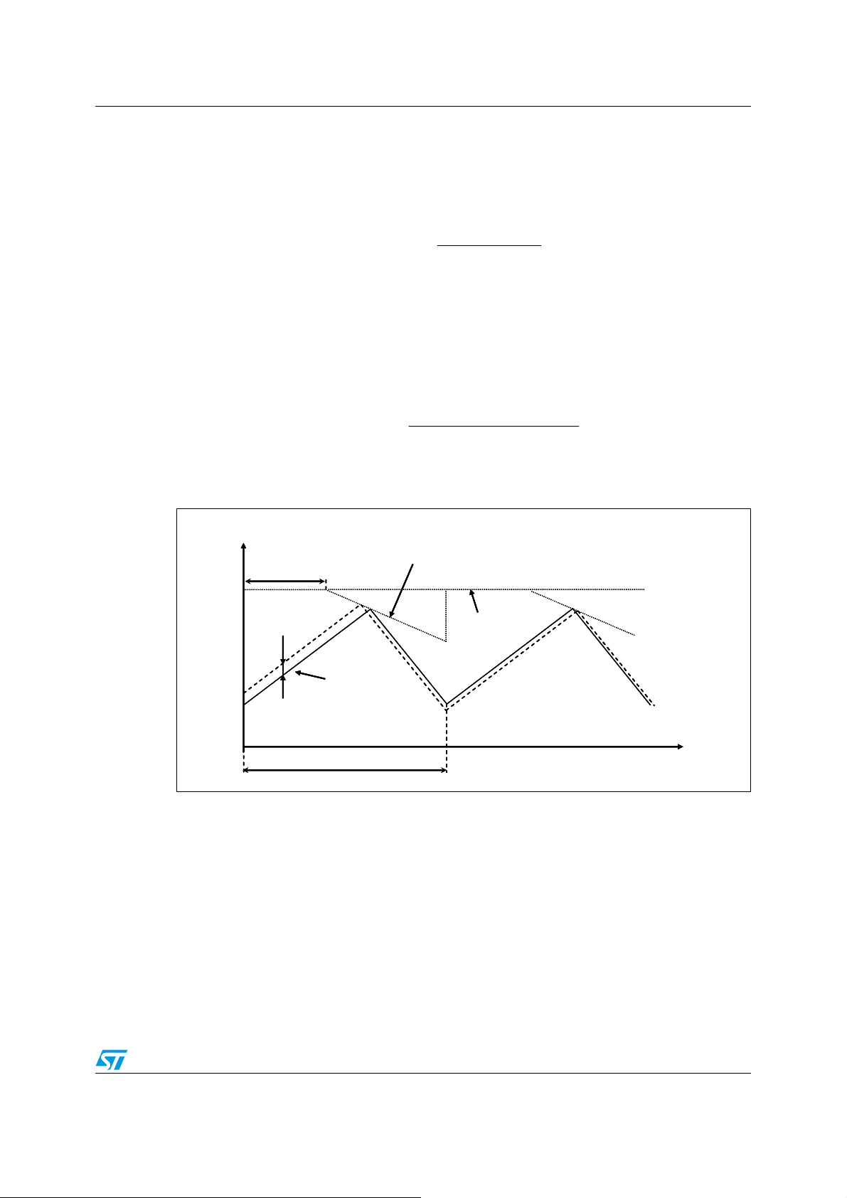
called “slope compensation”. In
the small perturbation ΔI
and the system reverts to a stable situation.
L
270ns minimum
270mV threshold
AM00604v1
Figure 12, where the switching duty-cycle is higher than 0.5,
dies away in subsequent cycles thanks to the slope compensation
16/46
Page 17
LED7706 Operation description
The SLOPE pin allows to properly set the amount of slope compensation connecting a
simple resistor R
between the SLOPE pin and the output. The compensation ramp
SLOPE
starts at 35% (typ.) of each switching period and its slope is given by the following equation:
Equation 6
⎞
VVV
−−
BEINOUT
⎟
⎟
⎠
Where KS = 5.8 ⋅10
10 s-1
⎛
⎜
KS
=
SE
⎜
R
⎝
, V
= 2 V (typ.) and SE is the slope ramp in [A/s].
BE
SLOPE
To avoid sub-harmonic instability, the compensating slope should be at least half the slope
of the inductor current during the off-phase when the duty-cycle is greater than 50%. The
value of
R
SLOPE
can be calculated according to equation 7.
Equation 7
)VVV(LK2
−−⋅⋅⋅
R
SLOPE
≤
−
INOUT
BEINOUTS
)VV(
Figure 12. Effect of slope compensation on small inductor current perturbation
(D > 0.5)
Inductor current (CCM)
Inductor current (CCM)
0.35
·T
0.35
·T
SW
SW
Programmed inductor peak current with
Programmed inductor peak current with
slope compensation (S
slope compensation (S
I
I
BOOST, PEAK
BOOST, PEAK
E)
E)
ΔI
ΔI
L
L
Inductor current
Inductor current
perturbation
perturbation
T
T
SW
SW
t
t
AM00606v1
17/46
Page 18
Operation description LED7706
5.1.7 Boost current limit
The design of the external components, especially the inductor and the flywheel diode, must
be optimized in terms of size relying on the programmable peak current limit. The LED7706
improves the reliability of the final application giving the way to limit the maximum current
flowing into the critical components. A simple resistor connected between the BILIM pin and
ground sets the desired value. The voltage at the BILIM pin is internally fixed to 1.23 V and
the current limit is proportional to the current flowing through the setting resistor, according
to the following equation:
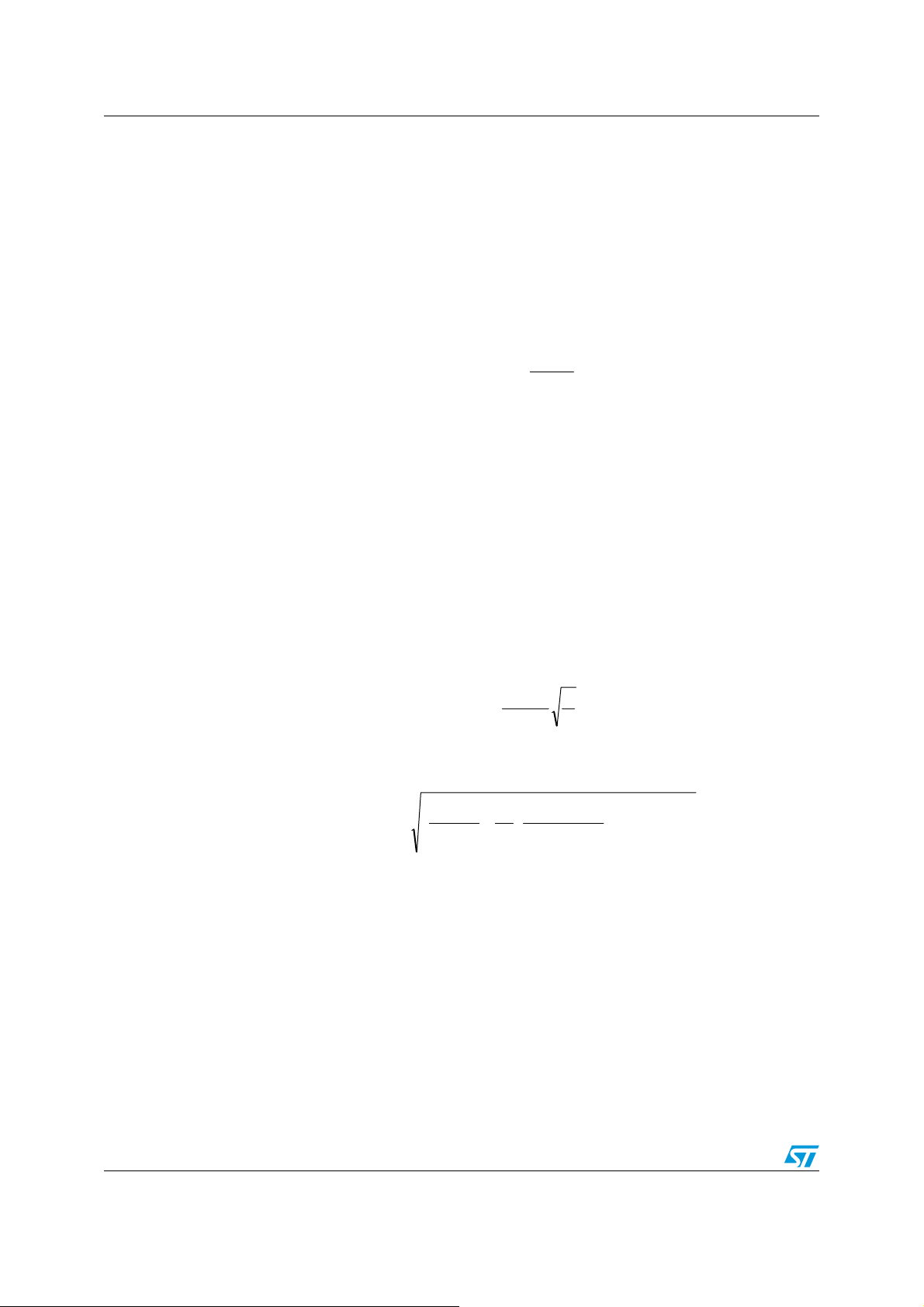
Equation 8
K
I =
PEAK,BOOST
where
B
The maximum allowed current limit is 5 A, resulting in a minimum setting resistor
R
> 120 kΩ. The maximum guaranteed RMS current in the power switch is 2 A.
BILIM
In a boost converter the RMS current through the internal MOSFET depends on both the
input and output voltages, according to equations 9a (DCM) and 9b (CCM).
B
R
BILIM
5
V106K
⋅=
The current limitation works by clamping the COMP pin voltage proportionally to R
Peak inductor current is limited to the above threshold decreased by the slope
compensation contribution.
Equation 9 a
Equation 9 b
5.1.8 Thermal protection
In order to avoid damage due to high junction temperature, a thermal shutdown protection is
implemented. When the junction temperature rises above 150 °C (typ.), the device turns off
both the control logic and the boost converter and holds the FAULT pin low. The LDO is kept
alive and normal operation is automatically resumed after the junction temperature has
been reduced by 30 °C.
.
BILIM
DV
⋅
I
rms,MOS
⎛
D
⎜
II
=
OUTrms,MOS
⎜
()
D1
−
⎝
IN
=
SW
⎛
1
⎜
+
⎜
2
12
⎝
D
3
LF
⋅
V
OUT
2
⎞
⎟
()()
⎟
LfI
⋅⋅
SWOUT
⎠
⎞
3
⎟
D1D
−
⎟
⎠
18/46
Page 19
LED7706 Operation description
5.2 Backlight driver section
5.2.1 Current generators
The LED7706 is a LEDs driver with six channels (rows); each row is able to drive multiple
LEDs in series (max. 36 V) and to sink up to 30 mA maximum current, allowing to manage
different kinds of LEDs.
The LEDs current can be set by connecting an external resistor (R
) between the RILIM
RILIM
pin and ground. The voltage across the RILIM pin is internally set to 1.23 V and the rows
current is proportional to the RILIM current according to the following equation:
Equation 10
K
I =
ROWx
R
R
RILIM
Where KR = 987 V.
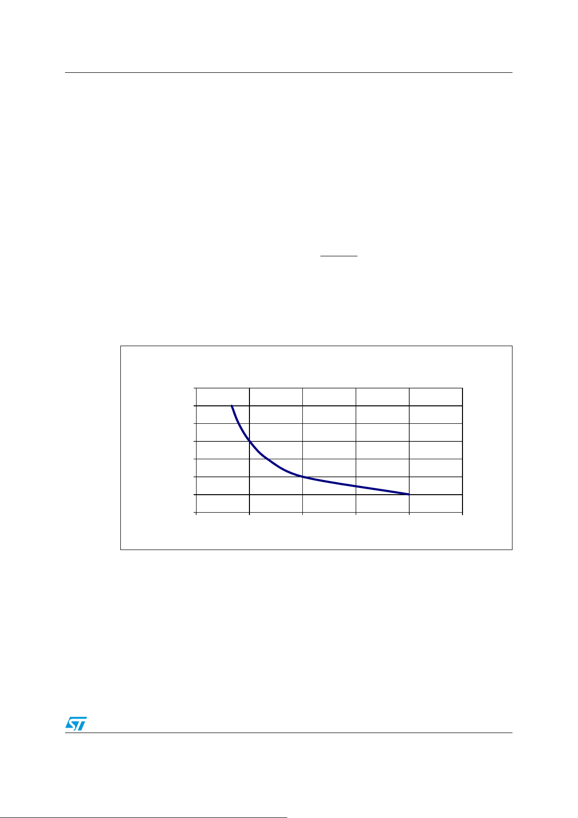
The graph in
Figure 13 better shows the relationship between I
ROW
and R
and helps to
RILIM
choose the correct value of the resistor to set the desired row current.
Figure 13. Row current vs R
35
30
25
20
15
RILIM
Row current vs R
RILIM
10
Row current [mA]
5
0
0 50 100 150 200 250
R
RILIM
[kΩ]
The maximum current mismatch between the rows is ± 2 % @ I
19/46
= 20 mA.
rowx
AM00605v1
Page 20
Operation description LED7706
⋅
=
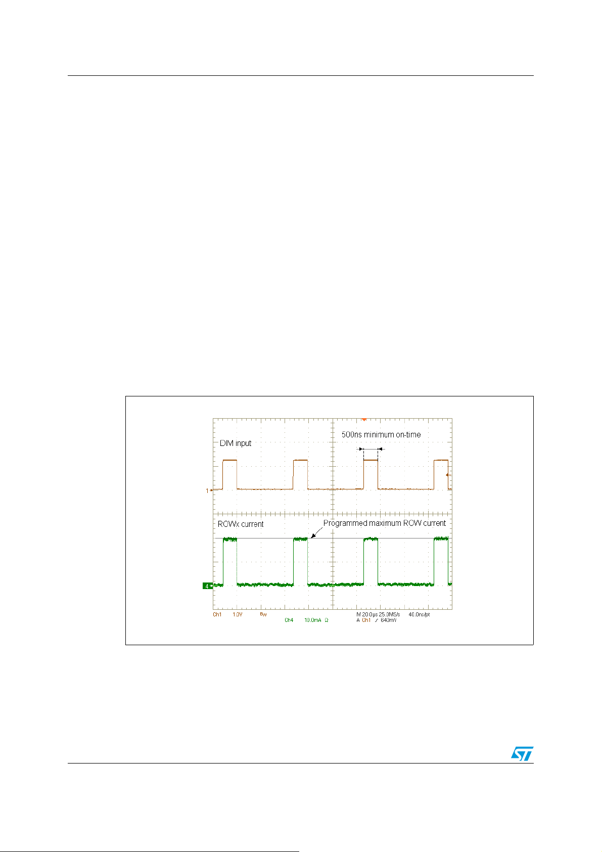
5.2.2 PWM dimming
The brightness control of the LEDs is performed by a pulse-width modulation of the rows
current. When a PWM signal is applied to the DIM pin, the current generators are turned on
and off mirroring the DIM pin behavior. Actually, the minimum dimming duty-cycle depends
on the dimming frequency.
The real limit to the PWM dimming is the minimum on-time that can be managed for the
current generators; this minimum on-time is approximately 500 ns.
Thus, the minimum dimming duty-cycle depends on the dimming frequency according to the
following formula:
Equation 11
fns500D
DIMmin,DIM
For example, at a dimming frequency of 20 kHz, 1% of dimming duty-cycle can be
managed.
During the off-phase of the PWM signal the boost converter is paused and the current
generators are turned off. The output voltage can be considered almost constant because of
the relatively slow discharge of the output capacitor. During the start-up sequence (see
Section 5.1.3 on page 13) the dimming duty-cycle is forced to 100% to detect floating rows
regardless of the applied dimming signal.
Figure 14. PWM dimming waveforms
20/46
Page 21
LED7706 Operation description
5.3 Fault management
The main loop keeps the row having the lowest voltage drop regulated to about 400 mV.
This value slightly depends on the voltage across the remaining active rows. After the softstart sequence, all protections turn active and the voltage across the active current
generators is monitored to detect shorted LEDs.
5.3.1 FAULT pin
The FAULT pin is an open-collector output, (with 4 mA current capability) active low, which
gives information regarding faulty conditions eventually detected. This pin can be used
either to drive a status LED or to warn the host system.
The FAULT pin status is strictly related to the MODE pin setting (see
5.3.2 MODE pin
The MODE pin is a digital input and can be connected to AVCC or SGND in order to choose
the desired fault detection and management. The LED7706 can manage a faulty condition
in two different ways, according to the application needs.
device detects and handles the internal protections related to the boost section (overcurrent, over-temperature and over-voltage) and to the current generators section (open and
shorted LEDs).
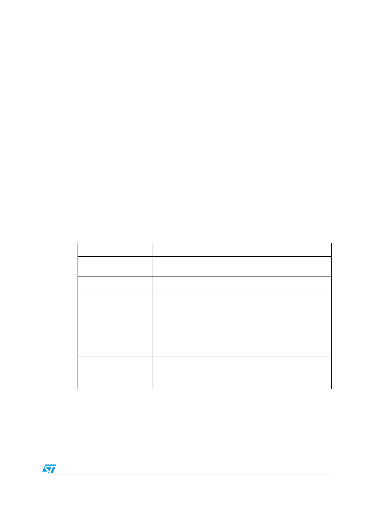
Table 6. Faults management summary
FAULT MODE to GND MODE to VCC
Internal MOSFET over
current
Output over voltage
Thermal shutdown
LED short shorted led
Open row(s)
FAULT pin HIGH
Power MOS turned OFF
FAULT pin LOW
Device turned OFF, latched condition
FAULT pin LOW. Device turned OFF.
Automatic restart after 30 C temperature drop.
FAULT pin LOW
Device turned OFF,
latched condition
(Vth = 3.4 V)
FAULT pin LOW
Device turned OFF at first
occurrence, latched condition
Ta bl e 6 for details).
Ta bl e 6 summarizes how the
FAULT pin LOW
Faulty row(s) disconnected
Device keeps on working with the
remaining row(s)
(Vth = 6 V)
FAULT pin HIGH Faulty row(s)
disconnected.
Device keeps on working with the
remaining row(s)
21/46
Page 22
Operation description LED7706
5.3.3 Open LED fault
In case a row is not connected or a LED fails open, the device has two different behaviors
according to the MODE pin status.
Connecting the MODE pin to SGND, as soon as an open row is detected the FAULT pin is
tied low and the device is turned off. The internal logic latches this status: to restore the
normal operation, the device must be restarted by toggling the EN pin or performing a
Power-On Reset (POR occurs when the voltage at the LDO5 pin falls below the lower UVLO
threshold and subsequently rises above the upper one).
If the MODE pin is high (i.e. connected to AVCC), the LED7706 behaves in a different
manner: the open row is excluded from the control loop and the device continues to work
properly with the remaining rows. The FAULT pin is not affected. Thus, if less than six rows
are used in the application, the MODE pin must be set high.
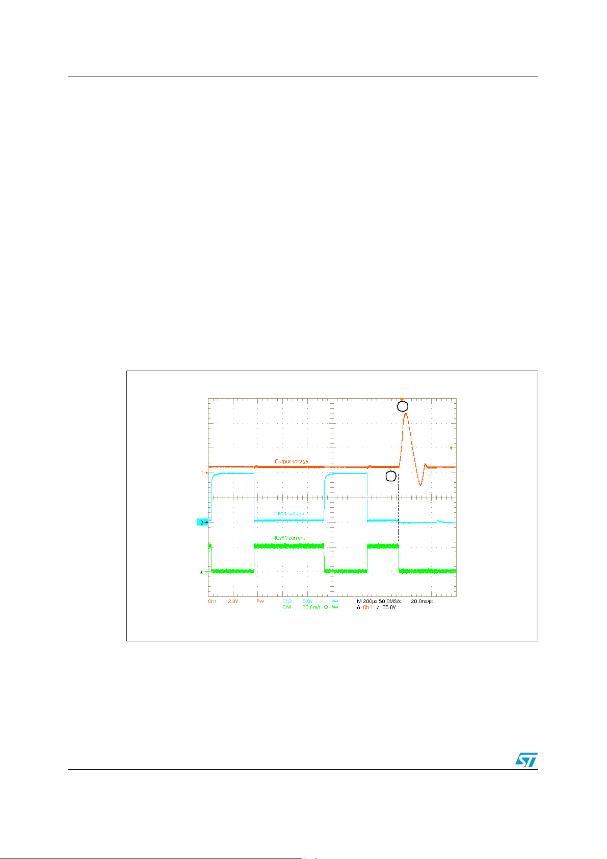
Figure 15 shows an example of open channel detection in case of MODE connected to
AVCC.
At the point marked as “1” in
point on the output voltage is increased as long as the output voltage reaches the floating
row detection threshold (see
faulty row is disconnected and the device keeps on working only with the remaining rows.
Figure 15. Open channel detection (MODE to AVCC)
Figure 15, the row opens (row current drops to zero). From this
Section 5.1.3 on page 13). Then (point marked as “2”) the
2
121
22/46
Page 23
LED7706 Operation description
5.3.4 Shorted LED fault
When a LED is shorted, the voltage across the related current generator increases of an
amount equal to the missing voltage drop of the faulty LED. Since the feedback voltage on
each active generator is constantly compared with a fault threshold V
TH,FAULT
detects the faulty condition and acts according to the MODE pin status.
, the device
If the MODE pin is low, the fault threshold is V
TH,FAULT
= 3.4 V. When the voltage across a
row is higher than this threshold, the FAULT pin is set low and the device is turned off. The
internal logic latches this status until the EN pin is toggled or a POR is performed.
In case the MODE pin is connected to AVCC, the fault threshold is set to 6 V. The LED7706
simply disconnects the rows whose voltage is higher than the threshold and the FAULT pin
is forced low. This option is also useful to avoid undesired triggering of the shorted-LED
protection simply due to the high voltage drop spread across the LEDs.
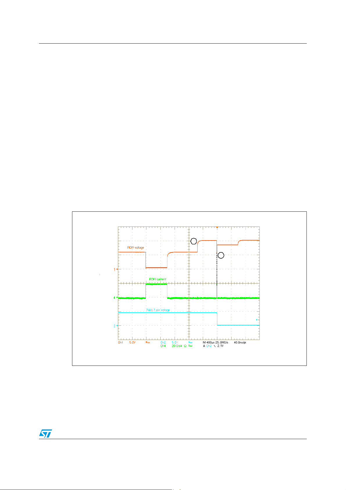
Figure 16 shows an example of shorted LED detection in case MODE is connected to GND.
At the point marked as “1” in
Figure 16 one LED fails becoming a short-circuit. The voltage
across the current generator of the channel where the failed LED is connected increases by
an amount equal to the forward voltage of the faulty LED. Since the voltage across the
current generator is above the threshold (3.4 V in this case), the device is turned off and the
fault pin is set low (point “2”).
Figure 16. Shorted LED detection (MODE to GND)
121
2
23/46
Page 24

Application information LED7706
⋅
≤
6 Application information
6.1 System stability
The boost section of the LED7706 is a fixed frequency, current-mode converter. During
normal operation, a minimum voltage selection circuit compares all the voltage drops across
the active current generators and provides the minimum one to the error amplifier. The
output voltage of the error amplifier determines the inductor peak current in order to keep its
inverting input equal to the reference voltage (400 mV typ). The compensation network
consists of a simple RC series (R
The calculation of R
COMP
dynamic performance of the boost converter and is strictly related to the operating
conditions.
6.1.1 Loop compensation
The compensation network can be quickly calculated using equations 12 to 16. Once both
R
get the optimal dynamic performance from the application.
The first parameter to be fixed is the switching frequency. Normally, a high switching
frequency allows reducing the size of the inductor and positively affects the dynamic
response of the converter (wider bandwidth) but increases the switching losses. For most of
applications, the fixed value (660 kHz) represents a good trade-off between power
dissipation and dynamic response, allowing to save an external resistor at the same time. In
low-profile applications, the inductor value is often kept low to reduce the number of turns;
an inductor value in the 4.7 µH-15 µH range is a good starting choice.
COMP
and C
have been determined, a fine-tuning phase may be required in order to
COMP
and C
- C
COMP
is fundamental to achieve optimal loop stability and
COMP
) between the COMP pin and ground.
COMP
In order to avoid instability due to interaction between the DC-DC converter's loop and the
current generators' loop, the bandwidth of the boost should not exceed the bandwidth of the
current generators. A unity-gain frequency (f
) in the order of 30-40 kHz is acceptable. Also,
U
take care not to exceed the CCM-mode right half-plane zero (RHPZ).
Equation 12
F2.0f
SWU
Equation 13
OUT
2
⎞
min,IN
⎟
⎟
⎠
⋅π
⎞
⎛
V
OUT
⎟
⎜
⎟
⎜
I
OUT
⎠
⎝
L2
V
⎛
⎜
2
RM
2.0f
U
⋅≤
L2
⋅π
⎜
V
⎝
2.0
⋅=
Equation 14 a
V
V
min,IN
OUT
M =
24/46
Page 25

LED7706 Application information
(
)
⋅⋅π
Equation 14b
V
OUT
R =
I
OUT
Where V
is the minimum input voltage and I
IN,min
is the overall output current.
OUT
Note that, the lower the inductor value (and the higher the switching frequency), the higher
the bandwidth can be achieved. The output capacitor is directly involved in the loop of the
boost converter and must be large enough to avoid excessive output voltage drop in case of
a sudden line transition from the maximum to the minimum input voltages.
However a more significant requirement concerns the output voltage ripple.
The output capacitor should be chosen in accordance with the following expression:
Equation 15
TII
⋅−
OFFOUTpeak,L
max,OUT
is the peak
L, peak
where ΔV
OUT, max
inductor current, T
C
>
OUT
V2
Δ⋅
is the maximum acceptable output voltage ripple, I
is the off-time of the switching cycle (for an extensive explanation see
OFF
Section 6.4.4 on page 31).
Once the output capacitor has been chosen, the R
can be calculated as:
COMP
Equation 16
Cf2
R
COMP
=
U
MgG
⋅⋅
EAM
Where GM = 2.7 S and g
Equation 16 places the loop bandwidth at f
= 375 µS
EA
. Then, the C
U
capacitor is determined to
COMP
place the frequency of the compensation zero 5 times lower than the loop bandwidth:
Equation 17
C
COMP
=
1
Rf2
⋅⋅π
COMPZ
Where fZ=fU/5.
In most of the applications an experimental approach is also very valid to compensate the
circuit. A simple technique to optimize different applications is to choose C
and to replace R
with a 10 kΩ trimmer adjusting its value to properly damp the output
COMP
COMP
= 4.7 nF
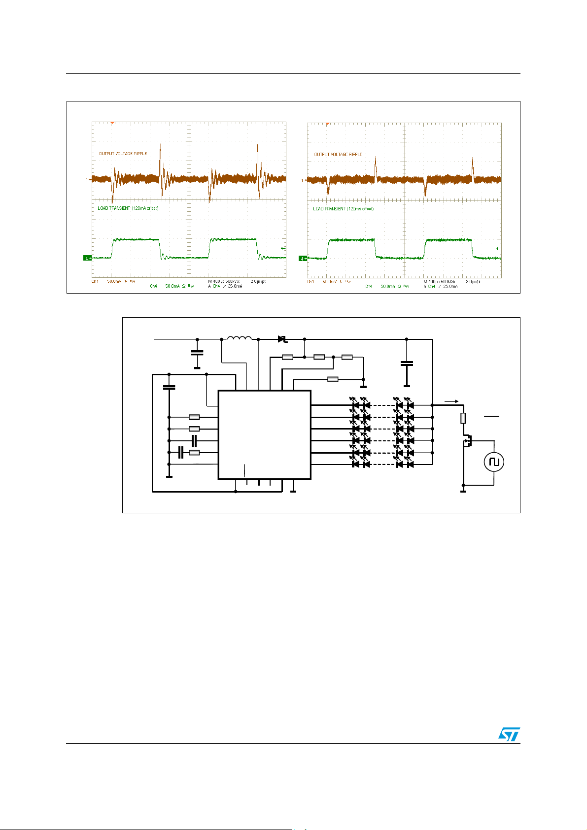
transient response. Insufficient damping will result in excessive ringing at the output and
poor phase margin.
Figure 17 (a and b) give an example of compensation adjustment for a typical application.
25/46
Page 26
Application information LED7706
Figure 17. Poor phase margin (a) and properly damped (b) load transient responses
a) b)
Figure 18. Load transient response measurement set-up
VIN= 6V
+5V
6.8μH
C
IN
LX
VIN
LDO5
BILIM
RILIM
SS
COMP
SGND
AVCC
LED7706
DIM
FAULT
EN
FSW
OVSEL
SLOPE
ROW1
ROW2
ROW3
ROW4
ROW5
ROW6
PGND
SYNC
MODE
Up to 10 WLEDs per row
V
4.7μF
MLCC
BOOST
R
=
L
500Hz
V
BST
50mA
AM00607v1
26/46
Page 27

LED7706 Application information
⋅+=
⋅⋅=
6.2 Thermal considerations
In order to prevent the device from exceeding the thermal shutdown threshold (150 °C), it is
important to estimate the junction temperature through the following equation:
Equation 18
PRTT
tot,DJA,thAmbJ
where TA is the ambient temperature, R
ambient and P
The R
measured on the application demonstration board (described in Section 6.5)
th,JA
is the power dissipated by the device.
D,tot
is the equivalent thermal resistance junction to
th,JA
is 42 °C/W.
The P
has several contributions, listed below.
D,tot
a) Conduction losses due to the R
of the internal power switch, equal to:\
DS(on)
Equation 19
2
DDIRP ⋅⋅⋅=
INDSoncond,D
DIM
where D is defined as:
Equation 20
V
IN
1D −=
V
OUT
and D
is the duty cycle of the PWM dimming signal.
DIM
b) Switching losses due to the power MOSFET turn on and off, calculated as:
Equation 21
)tt(
+
fr
fIVP ⋅
⋅⋅⋅=
swINOUTsw,D
D
2
DIM
where tr and tf are the power MOSFET rise time and fall time respectively.
c) Current generators losses. This contribution is strictly related to the LEDs used in
the application. Only the contribution of the leading current generator (“master”
current generator) can be predicted, regardless of the LEDs forward voltage:
Equation 22
DVIP
DIMIFBROWMaster,GEN
where I
is the current flowing through the row, whereas V
ROW
is the voltage across the
IFB
master current generator (typically 400 mV).
The voltages across the other current generators depend on the spread of the LEDs forward
voltage. The worst case for power dissipation (maximum forward voltage LEDs in the master
row, minimum forward voltage LEDs in all other rows) can be estimated as:
27/46
Page 28
Application information LED7706
(
(
)
⋅⋅Δ+⋅−⋅
(
⋅−=
Equation 23
=
where n
voltage and n
d) LDO losses, due to the dissipation of the 5 V linear regulator:
Equation 24
The LED7706 is housed in a 24 leads 4x4-VFQFPN package with exposed pad that allows
good thermal performance. However it is also important to design properly the
demonstration board layout in order to assure correct heat dissipation.
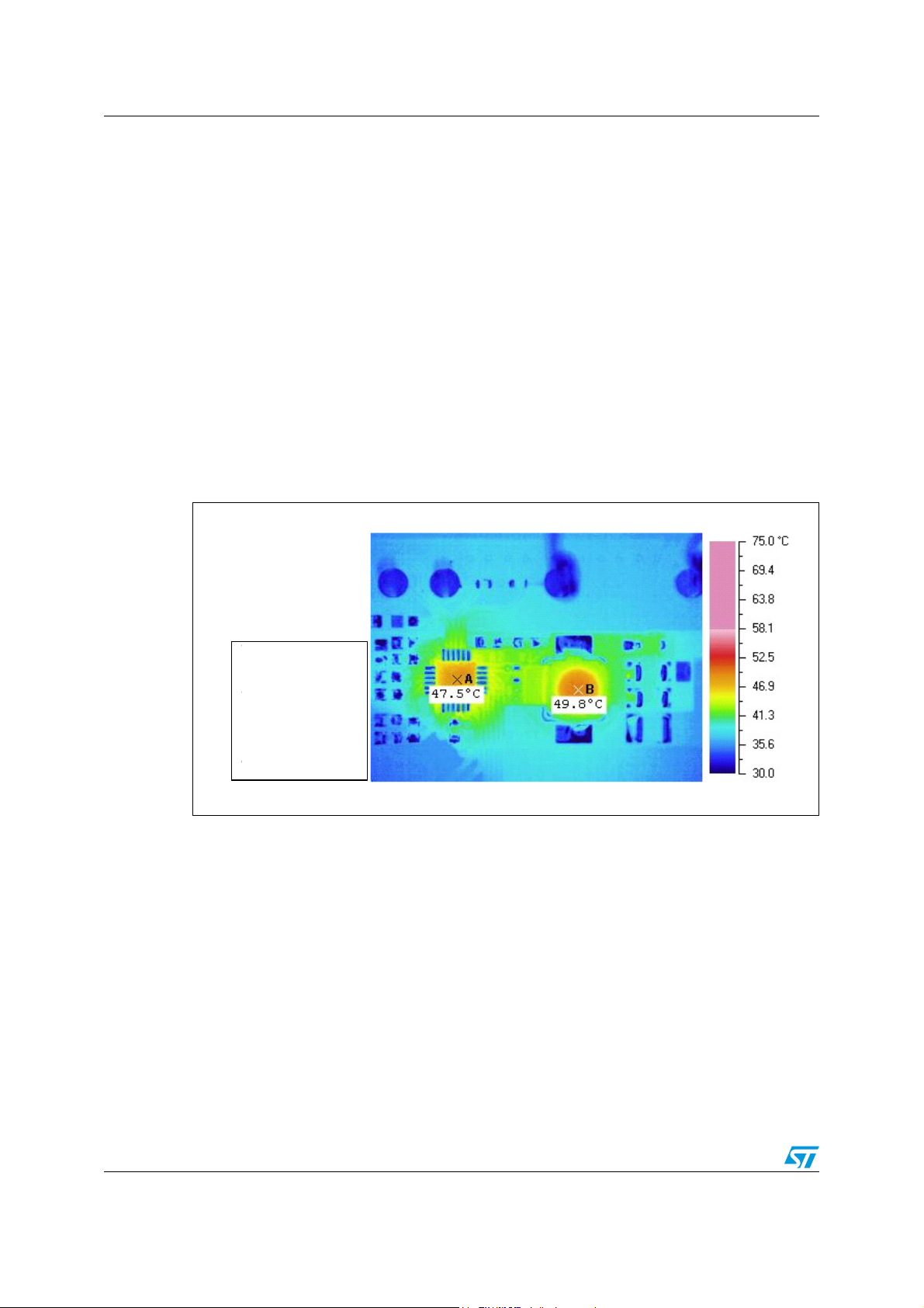
Figure 19 shows a picture of the LED7706 application demonstration board taken using an
infrared camera. The chip temperature, in those application conditions, is kept below 50 °C.
Figure 19. Demonstration board thermographic analysis
is the number of active rows, ΔV
ROWs
is the number of LEDs per row.
LEDs
)
is the spread of the LEDs forward
f,LEDs
)
IVVP
LDOLDOINLDO,D
DnVV1nIP
DIMLEDsLEDs,fIFBROWsROWGEN
VIN= 12V
VIN= 12V
= 20m A
= 20m A
I
I
ROW
ROW
= 34V
= 34V
V
V
OUT
OUT
= 660kHz
= 660kHz
F
F
SW
SW
= 90%
= 90%
D
D
DIM
DIM
= 30°C
= 30°C
T
T
Amb
Amb
6.3 Component selection
6.3.1 Inductor selection
Being the LED7706 mostly dedicated to backlighting, real-estate applications dictate severe
constrain in selecting the optimal inductor. The inductor choice must take into account
different parameters like conduction losses (DCR), core losses (ferrite or iron-powder),
saturation current and magnetic-flux shielding (core shape and technology).
The switching frequency of the LED7706 can be set in the 200 kHz-1 MHz range, allowing a
wide selecting room for the inductance value. Low switching frequencies takes to high
inductance value, resulting in significant DCR and size. On the other hand, high switching
frequencies result in significant core losses. The suggested range is 4.7-22 µH, even if the
28/46
Page 29
LED7706 Application information
best trade off between the different loss contributions varies from manufacturer to
manufacturer.
A 6.8 µH inductor has been experimentally found as the most suitable for applications
running at a 660 kHz switching frequency.
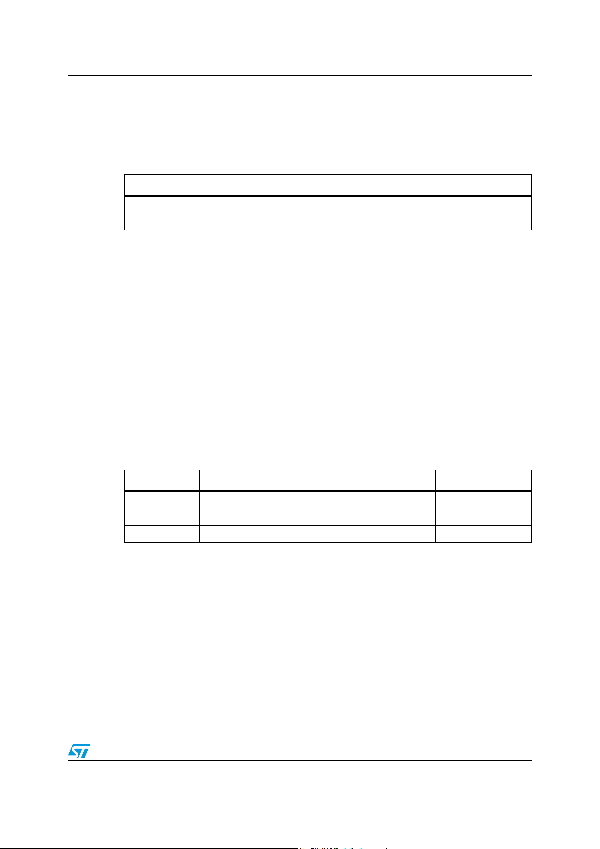
Table 7. Recommended inductors
Manufacturer Part number Description Size
Coilcraft LPS6235-682MLC 6.8 μH, 75 mΩ, 2.7 A 6x6 mm
Wurth 7440650068 6.8 μH, 33 mΩ, 3.6 A 10x10 mm
6.3.2 Capacitors selection
The input and output capacitors should have very low ESR (ceramic capacitors) in order to
minimize the ripple voltage. The boost converter of the LED7706 has been designed to
support ceramic capacitors. The required capacitance depends on the programmed LED
current and the minimum dimming frequency (the boost converter is off when the DIM pin is
low and the output capacitor is slowly discharged). Considering the worst case (i.e. 200 Hz
dimming frequency and 30 mA/channel), two 2.2 µF MLCCs are suitable for almost all
applications. Particular care must be taken when selecting the rated voltage and the
dielectric type of the output capacitors: 50 V rated MLCC may show a significant
capacitance drop when biased, especially in case of Y5V dielectric.
As in most of boost converters, the input capacitor is less critical, although it is necessary to
reduce the switching noise on the supply rail. The input capacitor is also important for the
internal LDO of the LED7706 and must be kept as close as possible to the chip. The rated
voltage of the input capacitor can be chosen according to the supply voltage range; a 10 µF
X5R MLCC is recommended.
Table 8. Recommended capacitors
Manufacturer Part number Description Package Notes
Taiyo Yuden UMK325BJ106KM-T Ceramic, 35V, X5R, 20 % SMD 1210 C
Murata GRM31CR71H225KA88B Ceramic, 50V, X7R, 20 % SMD 1206 C
Murata GRM31CR71H475KA88B Ceramic, 50V, X7R, 20 % SMD 1206 C
6.3.3 Flywheel diode selection
The flywheel diode must be a Schottky type to minimize the losses. This component is
subject to an average current equal to the output one and must sustain a reverse voltage
equal to the maximum output rail voltage. Considering all the channels sinking 30mA each
(i.e. 180 mA output current) and the maximum output voltage (36 V), the STP1L40M
(I
= 1 A, Vr = 40 V) diode is a good choice. Smaller diodes can be used in applications
f,ave
involving lower output voltage and/or lower output current.
IN
OUT
OUT
29/46
Page 30

Application information LED7706
(
6.4 Design example
In order to help the design of an application using the LED7706, in this section a simple
step-by-step design example is provided.
A possible application could be the LED backlight in a 15” LCD panel using the LED7706.
Here below the possible application conditions are listed:
● V
● 2 strings of 48 white LEDs (20 mA) each (arranged in 6 rows, 8 LEDs per row)
● V
6.4.1 Switching frequency setting
To reduce the number of the external components, the default switching frequency is
selected (660 kHz typ.) by connecting the FSW pin to AVCC pin.
However, in case a different switching frequency is required, a resistor from FSW pin and
ground can be connected, according to the equation (5) in
6.4.2 Row current setting
= 12 ± 20 %
IN
= 3.5 V ± 200 mV
F, L ED s
Section 5.1.5.
Considering the equation 10 in Section 5.2.1, the R
Equation 25
The closest standard commercial value is 51 kΩ. The actual value of the row current will be
a little lower (19.3 mA).
6.4.3 Inductor choice
The boost section, as all DC-DC converters, can work in CCM (continuous conduction
mode) or in DCM (discontinuous conduction mode) depending on load current, input and
output voltage and other parameters, among which the inductor value.
In a boost converter it is usually preferable to work in DCM.
Once the load, the input and output voltage, and the switching frequency are fixed, the
inductor value defining the boundary between DCM and CCM operation can be calculated
as:
Equation 26
R
RILIM
K
I
ROW
L
resistor can be calculated as:
RILIM
R
0
=
B
V987
mA20
2
)
D1DR
−⋅⋅
F2
⋅
SW
Ω=== k35.49
where D is the duty-cycle defined as:
30/46
Page 31

LED7706 Application information
=⋅=
=+⋅
=
(
)
μ=<
Equation 27
=
⎧
V
IN
V
OUT
=−=
⎨
⎩
1D
min,IN
max,IN
V6.9V@68.0
=
V4.14V@52.0
whereas R0 is:
Equation 28
V
R
OUT
0
I
OUT
Ω== 250
and
Equation 29
ROWOUT
mA120I6I
The output voltage in the above calculations is considered as the maximum value (LED with
the maximum forward voltage connected to the leading generator):
Equation 30
max,LEDs,Fmax,OUT
V30mV400V8V
Considering the input voltage range, the lower LB will be at the lower input voltage. Hence
the condition to assure the DCM operation becomes:
Equation 31
min,INB
H2.13VLL
An inductor value of 6.8 µH could be a suitable value, considering also a margin from the
boundary condition.
It is important to highlight that the inductor choice involves not only the value itself but the
saturation current (higher than the current limit, see
Section 6.4.4), the rated RMS current
(the compliance with the saturation current might be not enough; also the thermal
performances must be taken into account), the DCR (which affects the efficiency) and the
size (in some application might be a strict requirement).
However the DCR can’t be reduced keeping the size small. Hence a trade off between these
two requirements must be achieved according to the application.
6.4.4 Output capacitor choice
The choice of the output capacitor is mainly affected by the desired output voltage ripple.
Since the voltage across the LEDs can be considered almost constant, this ripple is
transferred across the current generators, affecting their dynamic response.
The output ripple can be estimated as (neglecting the contribution of ESR of C
in case of MLCC):
31/46
, very low
OUT
Page 32
Application information LED7706
(
)
Equation 32
⋅−
TII
OUT
OFFOUTpeak,L
`
V
OUT
=Δ
⋅
C2
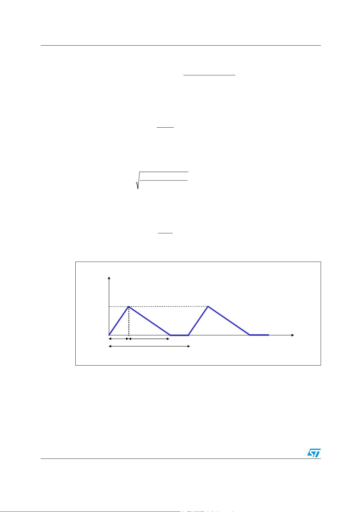
where I
is the inductor peak current (see Figure 20) calculated as:
L, peak
Equation 33
⎧
⋅
DV
IN
sw
=
⎨
⋅
LF
⎩
=
I
peak,L
whereas D, working in DCM, is:
Equation 34
⎧
−⋅⋅⋅
=
D
sw
R
0
)1M(MLF2
=
⎨
⎩
defining M as:
Equation 35
M
⎨
V
IN
⎩
⎧
V
OUT
=
Figure 20. Inductor current in DCM operation
=
min,IN
max,IN
=
min,IN
=
max,IN
V6.9V@A044.1
=
V4.14V@A914.0
=
min,IN
max,IN
V6.9V@488.0
=
V4.14V@285.0
V6.9V@125.3
V4.14V@083.2
I
L
I
L, peak
T
T
can be calculated as:
OFF
Equation 36
defining D2 as:
ON
T
OFF
TSW= 1/F
SW
=
⎧
=⋅=
DTT
⎨
2SWOFF
⎩
min,IN
max,IN
V6.9V@ns5.348
=
V4.14V@ns5.398
t
AM00608v1
32/46
Page 33

LED7706 Application information
(
)
Equation 37
=
⎧
⋅⋅⋅
MLF2
=
D
2
SW
()
0
=
−⋅
⎨
1MR
⎩
min,IN
max,IN
V6.9V@23.0
=
V4.14V@263.0
The worst case for the output voltage ripple is when input voltage is lower (V
A simple way to select the C
In order to affect as less as possible the current generators, it would be better to fix the
maximum ripple lower than the typical voltage across the generators.
For example considering
ΔV
leading generator), the required capacitance is:
Equation 38
A margin from the calculated value should be taken into account because of the
capacitance drop due to the applied voltage when MLCCs are used.
A 4.7 µF MLCC can be a good choice for this application (two 2.2 μF MLCC in parallel can
be also a good solution).
In case a dimming duty cycle different from 100 % is used, a further contribution to the
capacitor discharge (during the off time of the dimming cycle) should be considered.
6.4.5 Input capacitor choice
The input capacitor of a boost converter is less critical than the output capacitor, due to the
fact that the inductor is in series with the input, and hence, the input current waveform is
continuous.
IN,min
value is fixing a maximum voltage ripple.
OUT
lower than 80 mV (i.e. the 20 % of the voltage across the
OUT
TII
⋅−
C
>
OUT
V2
Δ⋅
OFFOUTpeak,L
max,OUT
F02.2
μ=
= 9.6 V).
A low ESR capacitor is always recommended.
A capacitor of 10 µF is tentatively a good choice for most of the applications.
6.4.6 Over-voltage protection divider setting
The over-voltage protection (OVP) divider provides a partition of the output voltage to the
OVSEL pin. The OVP divider setting not only fixes the OVP threshold, but also the openchannel detection threshold (95 % of the OVP threshold).
The proper OVP divider setting can be calculated by the equation (3):
Equation 39
RR
⋅=
where V
OUT, MAX
the maximum V
12
is the maximum output voltage considering the worst case (all LEDs with
= V
F
= 3.7 V on the same row):
F, m a x
MAX,OUT
33/46
V234.1
−+
)V234.1V2V(
Page 34

Application information LED7706
=+⋅
=
Equation 40
R1 can be chosen is in the order of hundreds of kilo-ohms to reduce the leakage current in
the resistor divider. For example, setting R
standard commercial value is R
The correct selection of the OVP divider (and, as consequence, the open channel detection
threshold) must take into account the shorted LED fault threshold (see
When the selected OVP threshold is too high, an undesired triggering of the shorted LED
detection circuitry may occur when a channel opens.
In fact, as explained in section 4.3.3, once a channel opens, the device reacts increasing the
output voltage and the voltage across the working current generators may reach the shorted
LED detection threshold before the open channel detection threshold.
6.4.7 Compensation network
For the compensation network, the suggestions provided in Section 6.1 are always valid.
In this condition, tentatively the following value of R3 and C8 (see
good choice for the loop stability:
R
= 2.4 kΩ
3
C
= 4.7 nF
8
= 22 kΩ.
2
max,FOVP,OUT
= 510 kΩ leads to R2 = 21.89 kΩ. The closest
1
V30mV400VnLEDV
Section 5.3.4).
Figure 23) are usually a
6.4.8 Boost current limit
The boost current limit is set to protect the internal power switch against excessive current.
The slope compensation may reduce the programmed current limit. Hence, to take into
account this effect, as a rule of thumb, the current limit can be set as twice as much the
maximum inductor peak current (see
I
BOOST, PEAK
Therefore, using equation (8) and choosing I
Equation 41
> 2.09 A
Section 6.4.4):
R
BILIM
BOOST, PEAK
K
I
= 2.5 A, R
B
PEAK,BOOST
Ω== k240
BILIM
will be:
34/46
Page 35

LED7706 Application information
=⋅⋅
=
(
)
⋅⋅Δ+⋅
−
=++
+
=⋅+
=
6.4.9 Power dissipation estimate
As explained in Section 6.2, there are several contributions to the total power dissipation.
Neglecting the power dissipated by the LDO (surely less significant compared with the other
contributions), equation (19), (21), (22) and (23) help to estimate the overall power
dissipation.
Before starting the power dissipation estimate it is important to highlight that the following
calculations are considering the worst case (the actual value of the dissipated power would
require measurements). Therefore the power dissipation is estimated according to the
following assumptions:
1. Minimum input voltage (9.6 V), which leads to maximum input current (and also D will
have the higher value, see
2. Maximum R
of the internal power MOSFET;
DS(on)
3. LEDs in the row of the leading generator will have the maximum forward voltage,
whereas all other LEDs in the other rows will have the minimum forward voltage.
4. 100 % dimming signal duty cycle is considered.
The conduction and switching losses on the internal power switch can be calculated as:
Equation 42
Section 6.4.4);
2
INDSoncond,D
DIM
mW34DDIRP
=⋅⋅⋅=
Equation 43
+
)tt(
fIVP
swINOUTsw,D
2
DIM
fr
⋅⋅⋅=
mW111D
=⋅
where tr = tf = 15 ns
The power dissipation related to the current generators is given by:
Equation 44
mW8DVIP
DIMIFBROWMaster,GEN
Equation 45
()
⋅=
DIMLEDsLEDs,fIFBROWsROWGEN
mW360DnVV1nIP
=
Equation 46
≅
GENMaster,GENsw,Dcond,Dtot,D
mW513PPPPP
The junction temperature can be estimated by equation (18) considering TA = 25 °C:
Equation 47
C5.46PRTT
tot,DJA,thAmbJ
35/46
°
Page 36

Application information LED7706
=⋅⋅
=
=++
=
In order to estimate also the efficiency, other contributions to the power dissipation must be
added to P
(which represents only the power dissipated by the device), that is:
D, t o t
Equation 48
mW5.34DIVP
where V
F, Diode
2INDiode,FDiode,DISS
= 0.4 V
Equation 49
2
RMS,IndInd,DISS
2
IN
mW2.11IDCRIDCRP
=⋅≅⋅=
where DCR = 80 mΩ (typical DCR of the recommended inductors).
Therefore the total dissipated power is:
Equation 50
Ind,DISSDiode,DISStot,DTOTAL,DISS
mW1.559PPPP
Considering the input power as the result of input voltage multiplied by the input current, the
estimated efficiency is:
Equation 51
PP
−
=η
TOT,DISSIN
P
IN
845.0
=
Note: It is important to remind that the previous calculations consider the worst case, especially for
the power dissipated on the current generators.
Statistical analysis (confirmed by bench measurements) shows that the series connection of
more LEDs on each channel leads to compensation effects.
The hypothesis 3 above mentioned is thus rather unlikely.
Therefore P
is significantly lower and the overall efficiency is typically around 90 %.
GEN
36/46
Page 37

LED7706 Application information
6.5 Layout consideration
1. A careful PCB layout is important for proper operation. In this section some guidelines
are provided in order to achieve a good layout.
2. The device has two different ground pins: signal ground (SGND) and power ground
(PGND). The PGND pin handles the switching current related to the boost section; for
this reason the PCB traces should be kept as short as possible and with adequate
width.
3. The signal ground is the return for the device supply and the current generators and
can be connected to the thermal pad.
4. The heat dissipation area (adequate to the application conditions) should be placed
backside respect to the device and with the lowest thermal impedance possible (i.e.
PCB traces in the backside should be avoided). The dissipation area is thermally and
electrically connected to the thermal pad by several vias (nine vias are recommended).
5. The signal and power grounds must be connected together in a single point as close as
possible to the PGND pin to reduce ground loops.
6. The R-C components of the compensation network should be placed as close as
possible to the COMP pin in order to avoid noise issue and instability of the
compensation.
7. Noise sensitive signals (i.e. feedbacks and compensation) should be routed as short as
possible to minimize noise collection. The LED7706 pinout makes it easy to separate
power components (e.g. inductor, diode) from signal ones.
8. The LX switching node should have and adequate width for high efficiency.
9. The critical power path inductor-LX-PGND must be as short as possible by mounting
the inductor, the diode and COUT as close as possible each other.
10. The capacitors of the compensated divider connected to the OVSEL pin should be
placed as close as possible to the OVSEL pin.
11. In order to assure good performance in terms of row current accuracy/mismatch, the
PCB traces from the rows pins to the LEDs should have similar length and width.
12. The capacitors of the filter connected to LDO5 and VIN pins should be mounted as
close as possible to the mentioned pins
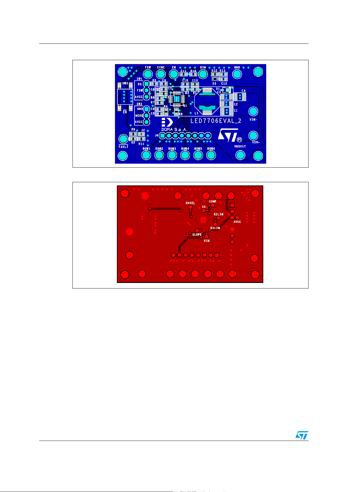
Figure 21 and Figure 22 shows the demonstration board layout (top view and bottom view
respectively).
37/46
Page 38
Application information LED7706
Figure 21. Demonstration board layout (top view)
Figure 22. Demonstration board layout (bottom view)
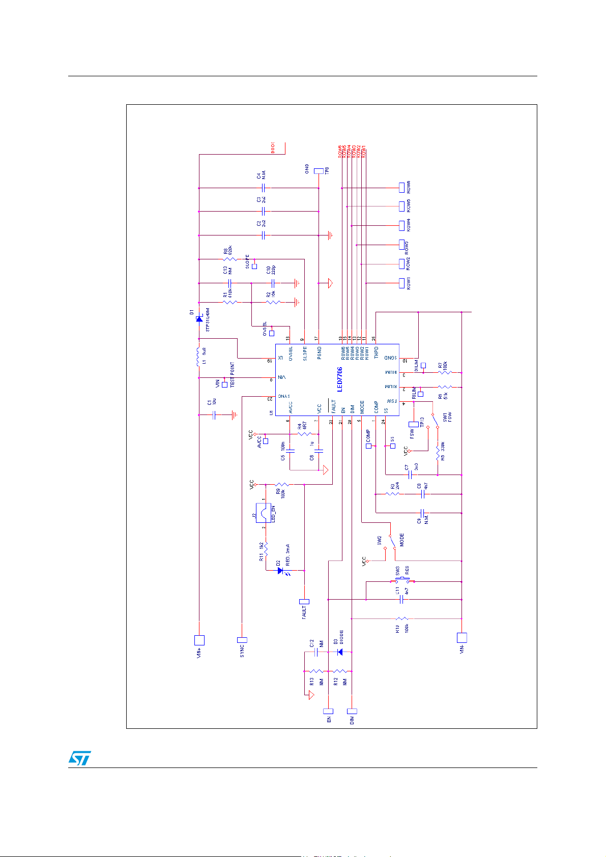
Figure 23
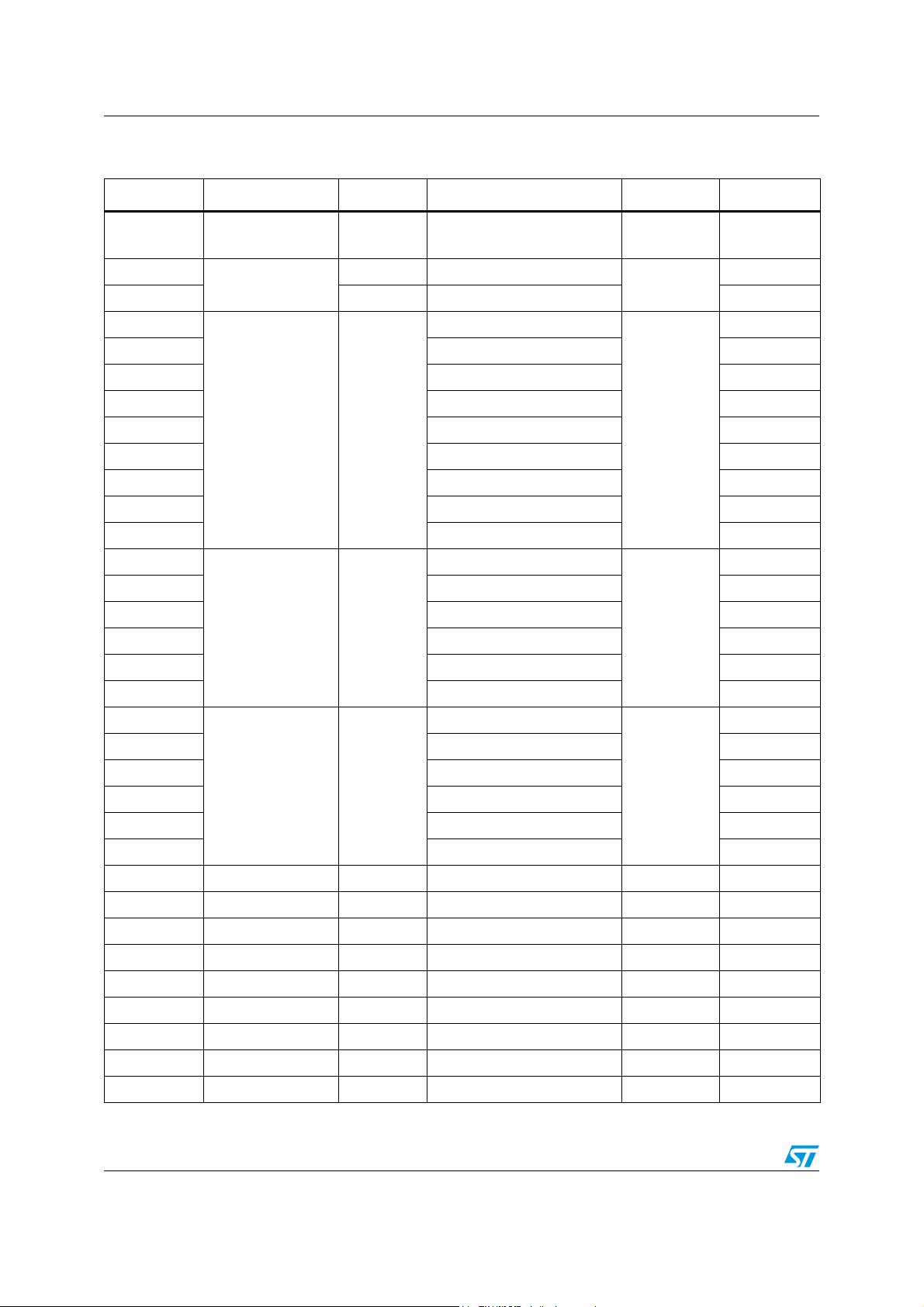
the used components and their value.
38/46
shows the LED7706 demonstration board application circuit, whereas Ta bl e 9 lists
Page 39
LED7706 Application information
Figure 23. LED7706 demonstration board schematic
AM00609v1
39/46
Page 40
Application information LED7706
Table 9. LED7706 demonstration board component list
Component Description Package Part number MFR Value
C1
C2,C3
C4 SMD 1206 GRM31CR71H225KA88B N.M.
C5
C6 100 nF
C7 3.3 nF
C8 4.7 nF
C9 N.M.
C10 220 pF
C11 4.7 nF
C12 N.M.
C13 15 pF
R1
R2 16 kΩ
R3 2.4 kΩ
R4 4.7 Ω
R5 330 kΩ
R6 51 kΩ
R7
Ceramic, 35V
X5R, 20%
Ceramic, 50V
X7R, 20%
Ceramic, 25V
X5R, 20%
Chip resistor
0.1 W, 1%
SMD 1210 UMK325BJ106KM-T Taiyo Yuden 10 µF
SMD 1206 GRM31CR71H225KA88B
Murata
SMD 0603 Standard
SMD 0603 Standard
2.2 µF
1 µF
510 kΩ
180 kΩ
R8 680 kΩ
R9, R10 100 kΩ
R11 1.2 kΩ
R12 N.M.
R13 N.M.
L1 6u8, 75 mΩ, 2.7 A 6x6 mm LPS6235-682MLC Coilcraft 6.8 µF
D1 Schottky, 40 V, 1 A DO216-AA STPS1L40M ST STPS1L40M
D2 Red LED, 3 mA SMD 0603 Standard
D3 Signal Schottky SOD-523 BAS69 N.M.
U1 Integrated circuit QFN4x4 LED7706 ST LED7706
J2 PCB pad jumper
J8 Header 8 SIL 8 Standard
SW1, SW2 Jumper 3 SIL 3 Standard
SW3 Push button 6x6 mm FSM4JSMAT TYCO
40/46
Chip resistor
0.1 W, 1%
SMD 0603 Standard
Page 41
LED7706 Electrical characteristics
7 Electrical characteristics
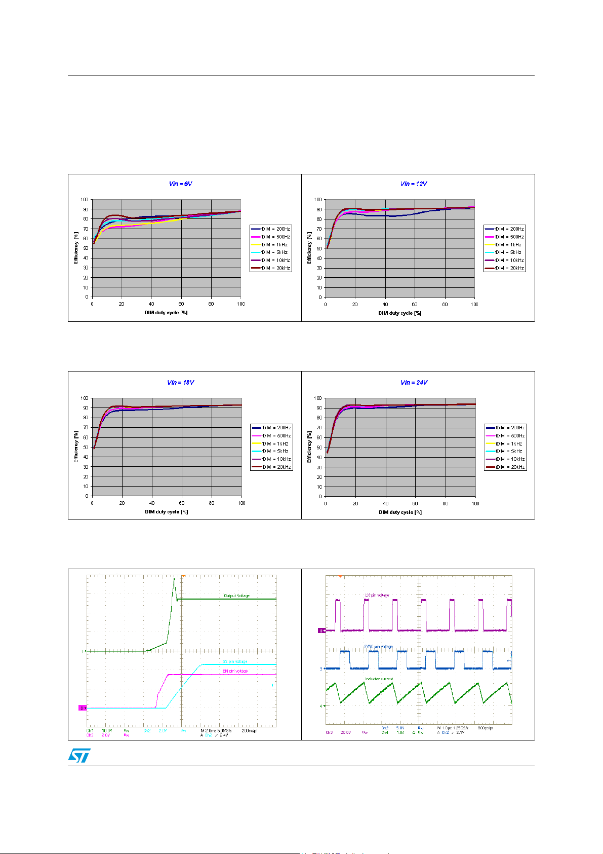
Figure 24. Efficiency versus DIM duty cycle,
V
= 6 V, 6 rows, 10 white LEDs
IN
(20 mA) in series
Figure 26. Efficiency versus DIM duty cycle,
V
= 18 V, 6 rows, 10 white LEDs
IN
(20 mA) in series
Figure 25. Efficiency versus DIM duty cycle,
VIN = 12 V, 6 rows, 10 white LEDs
(20 mA) in series
Figure 27. Efficiency versus DIM duty cycle,
VIN = 24 V, 6 rows, 10 white LEDs
(20 mA) in series
Figure 28. Soft-start waveforms (EN, SS, and
V
monitored)
OUT
Figure 29. Boost section switching signals
(LX, SYNC and inductor current
monitored), V
41/46
= 12 V, 10 LEDs
IN
Page 42
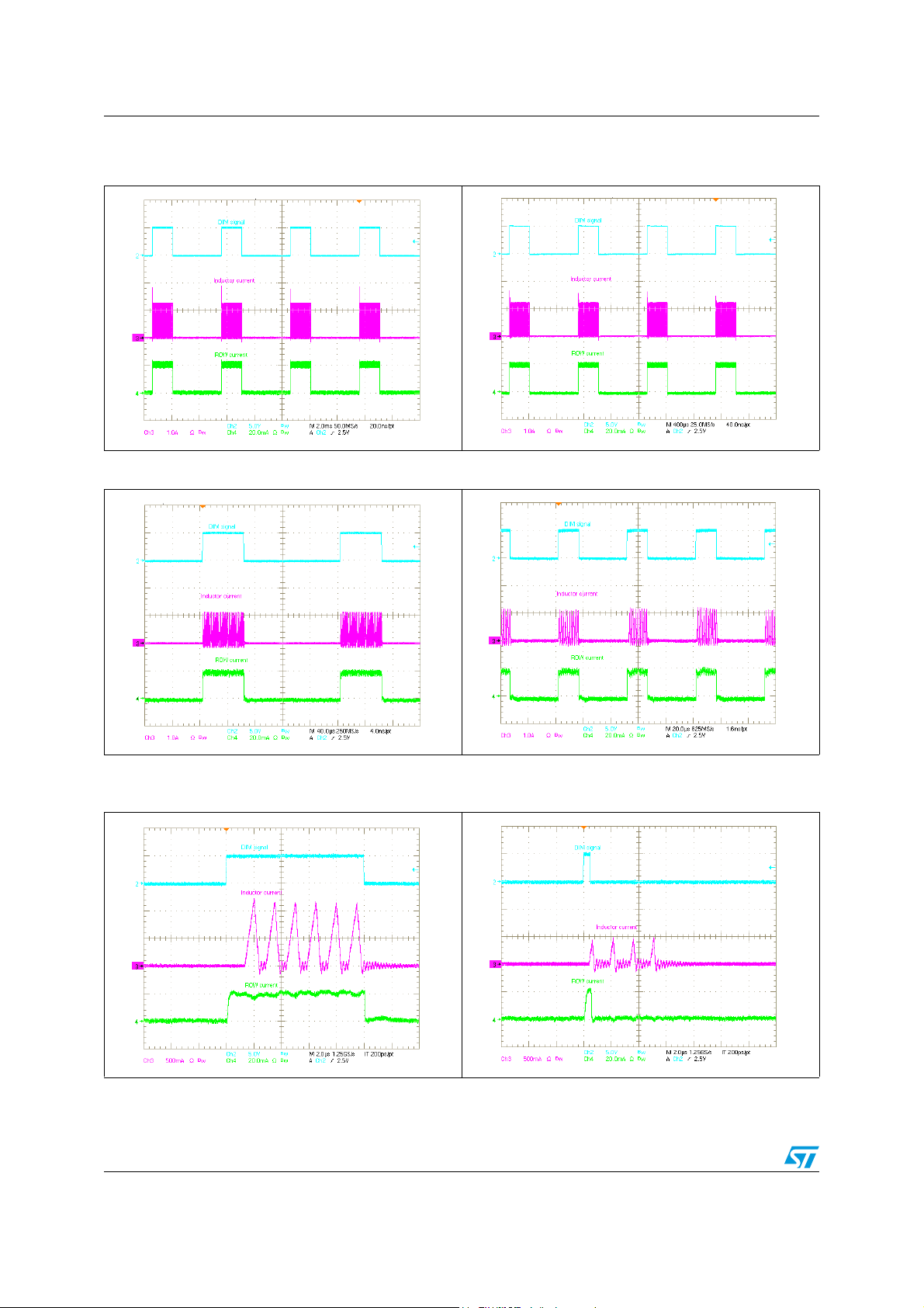
Electrical characteristics LED7706
Figure 30. Dimming waveforms
(F
= 200 Hz)
Figure 32. Dimming waveforms (F
DIM
= 5 kHz) Figure 33. Dimming waveforms (F
DIM
Figure 31. Dimming waveforms (F
= 1 kHz)
DIM
= 20 kHz)
DIM
Figure 34. Dimming waveforms
(T
42/46
DIM,ON
= 10 µs)
Figure 35. Dimming waveforms with the
minimum dimming on time (500 ns)
Page 43

LED7706 Package mechanical data
8 Package mechanical data
In order to meet environmental requirements, ST offers these devices in different grades of
ECOPACK
specifications, grade definitions and product status are available at: www.st.com.
ECOPACK
®
packages, depending on their level of environmental compliance. ECOPACK®
®
is an ST trademark.
43/46
Page 44
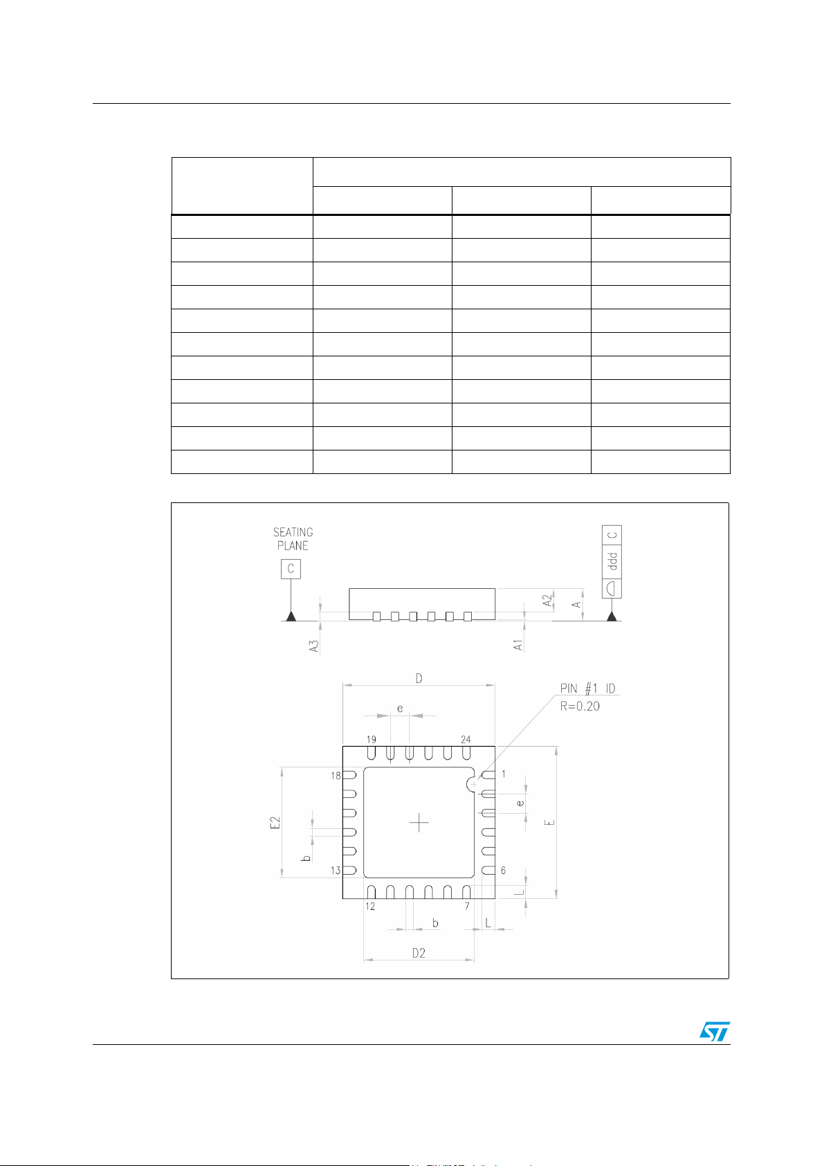
Package mechanical data LED7706
Table 10. VFQFPN-24 4 mm x 4 mm mechanical data
mm
Dim.
Min. Typ. Max.
A 0.80 0.90 1.00
A1 0.00 0.02 0.05
A3 0.20
b 0.18 0.25 0.30
D 3.85 4.00 4.15
D2 2.40 2.50 2.60
E 3.85 4.00 4.15
E2 2.40 2.50 2.60
e0.50
L 0.30 0.40 0.50
ddd 0.08
Figure 36. Package dimensions
44/46
Page 45
LED7706 Revision history
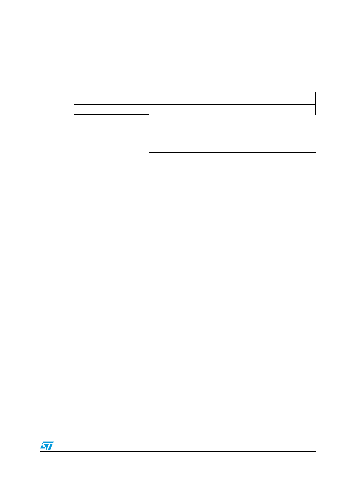
9 Revision history
Table 11. Document revision history
Date Revision Changes
08-Feb-2008 1 Initial release
Added: Chapter 3 on page 7, Chapter 3 on page 7 and Chapter 3 on
page 7
09-Apr-2009 2
Updated: Chapter 3 on page 7, Chapter 3 on page 7, Chapter 3 on
page 7, Ta bl e 4 , Tab l e 5 , Figure 3, Figure 4, Figure 7, Figure 23 and
Ta bl e 9
45/46
Page 46

LED7706
Please Read Carefully:
Information in this document is provided solely in connection with ST products. STMicroelectronics NV and its subsidiaries (“ST”) reserve the
right to make changes, corrections, modifications or improvements, to this document, and the products and services described herein at any
time, without notice.
All ST products are sold pursuant to ST’s terms and conditions of sale.
Purchasers are solely responsible for the choice, selection and use of the ST products and services described herein, and ST assumes no
liability whatsoever relating to the choice, selection or use of the ST products and services described herein.
No license, express or implied, by estoppel or otherwise, to any intellectual property rights is granted under this document. If any part of this
document refers to any third party products or services it shall not be deemed a license grant by ST for the use of such third party products
or services, or any intellectual property contained therein or considered as a warranty covering the use in any manner whatsoever of such
third party products or services or any intellectual property contained therein.
UNLESS OTHERWISE SET FORTH IN ST’S TERMS AND CONDITIONS OF SALE ST DISCLAIMS ANY EXPRESS OR IMPLIED
WARRANTY WITH RESPECT TO THE USE AND/OR SALE OF ST PRODUCTS INCLUDING WITHOUT LIMITATION IMPLIED
WARRANTIES OF MERCHANTABILITY, FITNESS FOR A PARTICULAR PURPOSE (AND THEIR EQUIVALENTS UNDER THE LAWS
OF ANY JURISDICTION), OR INFRINGEMENT OF ANY PATENT, COPYRIGHT OR OTHER INTELLECTUAL PROPERTY RIGHT.
UNLESS EXPRESSLY APPROVED IN WRITING BY AN AUTHORIZED ST REPRESENTATIVE, ST PRODUCTS ARE NOT
RECOMMENDED, AUTHORIZED OR WARRANTED FOR USE IN MILITARY, AIR CRAFT, SPACE, LIFE SAVING, OR LIFE SUSTAINING
APPLICATIONS, NOR IN PRODUCTS OR SYSTEMS WHERE FAILURE OR MALFUNCTION MAY RESULT IN PERSONAL INJURY,
DEATH, OR SEVERE PROPERTY OR ENVIRONMENTAL DAMAGE. ST PRODUCTS WHICH ARE NOT SPECIFIED AS "AUTOMOTIVE
GRADE" MAY ONLY BE USED IN AUTOMOTIVE APPLICATIONS AT USER’S OWN RISK.
Resale of ST products with provisions different from the statements and/or technical features set forth in this document shall immediately void
any warranty granted by ST for the ST product or service described herein and shall not create or extend in any manner whatsoever, any
liability of ST.
ST and the ST logo are trademarks or registered trademarks of ST in various countries.
Information in this document supersedes and replaces all information previously supplied.
The ST logo is a registered trademark of STMicroelectronics. All other names are the property of their respective owners.
© 2009 STMicroelectronics - All rights reserved
STMicroelectronics group of companies
Australia - Belgium - Brazil - Canada - China - Czech Republic - Finland - France - Germany - Hong Kong - India - Israel - Italy - Japan -
Malaysia - Malta - Morocco - Singapore - Spain - Sweden - Switzerland - United Kingdom - United States of America
www.st.com
46/46
 Loading...