

Datasheet LD29080DT15R, LD29080PT15R, LD29080PTR, LD29080DT18R, LD29080PT18R Datasheet (ST)
...Page 1
800 mA fixed and adjustable output very low drop
Features
■ Very low dropout voltage (typ. 0.4 at 800 mA)
■ Guaranteed output current up to 800 mA
■ Fixed and adjustable output voltage (± 1% at
25 °C)
■ Internal current and thermal limit
■ Logic controlled electronic shutdown
Description
LD29080xx
voltage regulator
Datasheet − production data
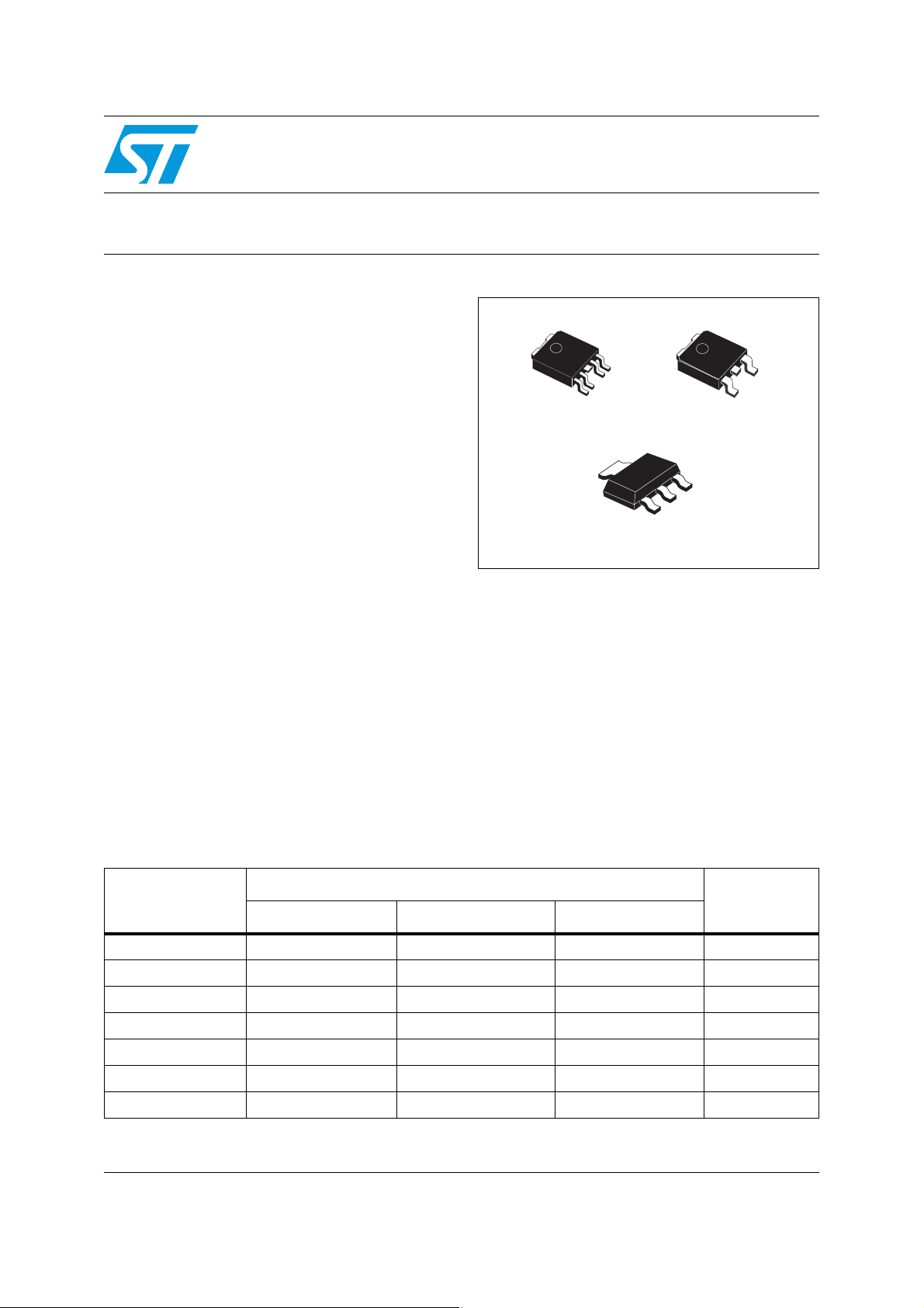
PPAK DPAK
The LD29080xx is a high current, high accuracy,
SOT223
low-dropout voltage regulators series. These
regulators feature 400 mV dropout voltages and
very low ground current. Designed for high
current loads, these devices also find applications
in lower current, extremely low dropout-critical
systems, where their tiny dropout voltage and
ground current values are important attributes.
Typical application are in power supply switching
post regulation, series power supply for monitors,
series power supply for VCRs and TVs, computer
systems and battery powered systems.
Table 1. Device summary
Order codes
Part numbers
DPAK (tape and reel) PPAK (tape and reel) SOT223
LD29080XX15 LD29080DT15R LD29080PT15R 1.5 V
LD29080XX18 LD29080DT18R LD29080PT18R 1.8 V
Output voltages
LD29080XX25 LD29080DT25R LD29080PT25R 2.5 V
LD29080XX33 LD29080DT33R LD29080PT33R LD29080S33R 3.3 V
LD29080XX50 LD29080DT50R LD29080PT50R 5.0 V
LD29080XX90 LD29080DT90R LD29080PT90R 9.0 V
LD29080XX LD29080PTR ADJ
May 2012 Doc ID 10918 Rev 7 1/24
This is information on a product in full production.
www.st.com
24
Page 2

Contents LD29080xx
Contents
1 Diagram . . . . . . . . . . . . . . . . . . . . . . . . . . . . . . . . . . . . . . . . . . . . . . . . . . . 3
2 Pin configuration . . . . . . . . . . . . . . . . . . . . . . . . . . . . . . . . . . . . . . . . . . . 4
3 Maximum ratings . . . . . . . . . . . . . . . . . . . . . . . . . . . . . . . . . . . . . . . . . . . . 5
4 Electrical characteristics . . . . . . . . . . . . . . . . . . . . . . . . . . . . . . . . . . . . . 6
5 Typical characteristics . . . . . . . . . . . . . . . . . . . . . . . . . . . . . . . . . . . . . . 14
6 Package mechanical data . . . . . . . . . . . . . . . . . . . . . . . . . . . . . . . . . . . . 17
7 Revision history . . . . . . . . . . . . . . . . . . . . . . . . . . . . . . . . . . . . . . . . . . . 23
2/24 Doc ID 10918 Rev 7
Page 3
LD29080xx Diagram
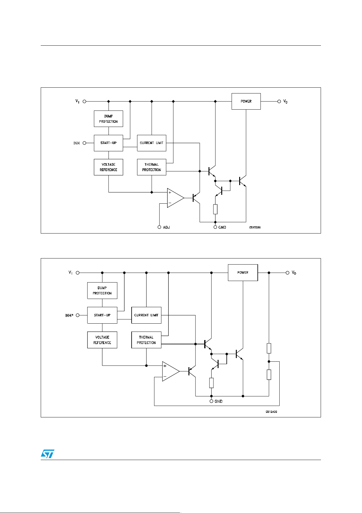
1 Diagram
Figure 1. Schematic diagram for adjustable version
Figure 2. Schematic diagram for fixed version
* Only for version with inhibit function.
Doc ID 10918 Rev 7 3/24
Page 4
Pin configuration LD29080xx
2 Pin configuration
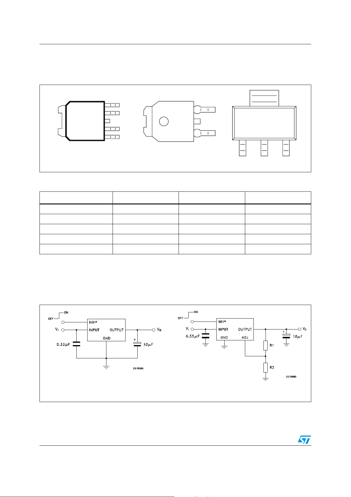
Figure 3. Pin connections (top view)
GND
PPAK
CS17230
5
4
3
GND
2
1
CS17240
DPAK
3
GND
2
1
123
AM09358v1
SOT223
Table 2. Pin description
Symbol PPAK DPAK SOT223
V
I
GND 3 2 2
V
O
ADJ/N.C.
INHIBIT
1. Not connect for fixed version.
2. Not internally pulled up; in order to assure the operating condition (device in ON mode), it must be connected to a positive
voltage higher than 2 V.
(1)
(2)
211
433
5
1
Figure 4. Application circuit
* Only for version with inhibit function.
4/24 Doc ID 10918 Rev 7
VO = V
(1 + R1/R2)
REF
Page 5
LD29080xx Maximum ratings
3 Maximum ratings
Table 3. Absolute maximum ratings
Symbol Parameter Value Unit
V
I
V
INH
I
O
P
D
T
STG
T
OP
1. Above 14 V the device is automatically in shut-down.
DC input voltage 30
Inhibit input voltage 14 V
Output current Internally limited mA
Power dissipation Internally limited mW
Storage temperature range - 55 to 150 °C
Operating temperature range - 40 to 125 °C
Note: Absolute maximum ratings are those values beyond which damage to the device may occur.
Functional operation under these conditions is not implied.
Table 4. Thermal data
(1)
V
Symbol Parameter DPAK PPAK SOT223 Unit
R
R
thJC
thJA
Thermal resistance junction-case 8 8 25 °C/W
Thermal resistance junction-ambient 100 100 110 °C/W
Doc ID 10918 Rev 7 5/24
Page 6
Electrical characteristics LD29080xx
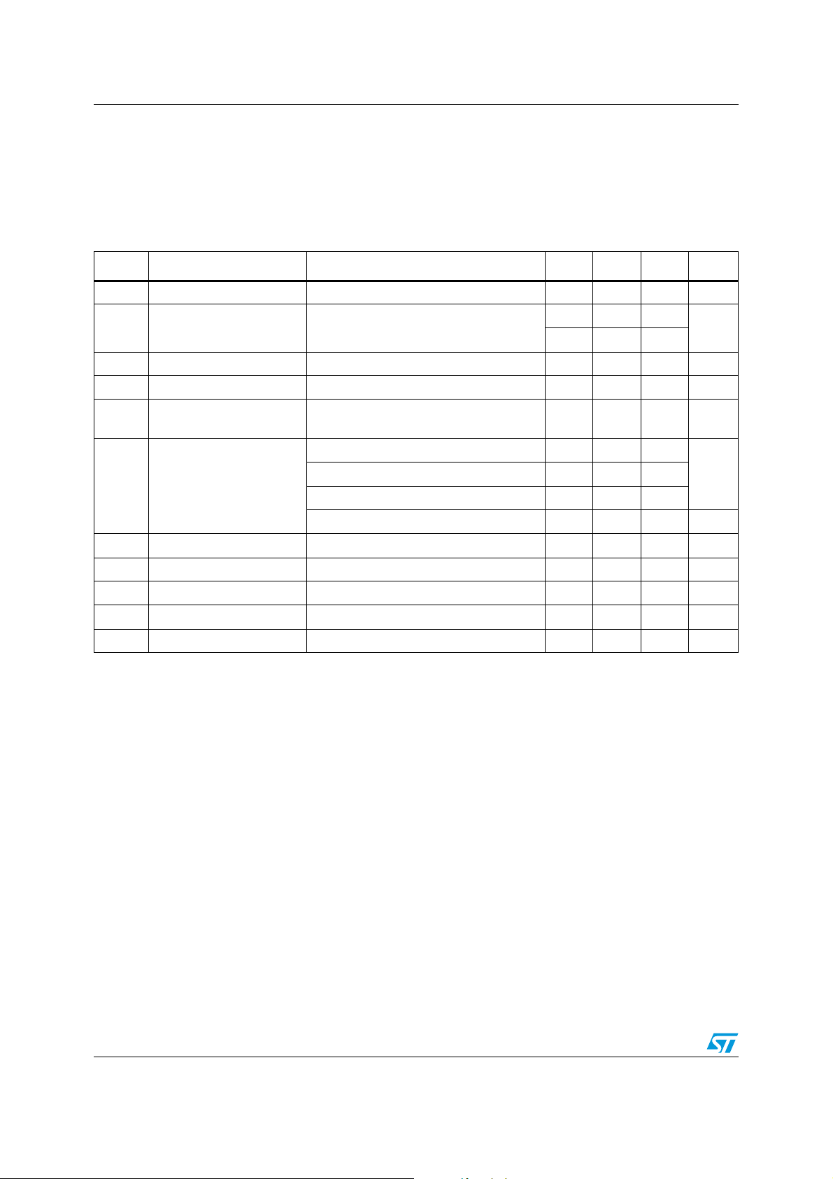
4 Electrical characteristics
IO = 10 mA, (
Note 4
) TJ = 25 °C, VI = 3.5 V, V
= 2V, CI = 330 nF, CO = 10 µF, unless
INH
otherwise specified.
Table 5. Electrical characteristics of LD29080#15
Symbol Parameter Test conditions Min. Typ. Max. Unit
V
I
V
O
ΔV
O
ΔV
O
SVR Supply voltage rejection
I
q
I
sc
V
IL
V
IH
I
INH
eN Output noise voltage BP = 10Hz to 100kHz, IO = 100mA 60 µV
Operating input voltage IO = 10mA to 800mA 2.5 13 V
Output voltage
= 10mA to 800mA, VI = 3 to 7V
I
O
= -40 to 125°C
T
J
1.485 1.5 1.515
1.463 1.537
Load regulation IO = 10mA to 800mA 0.2 1.0 %
Line regulation VI = 3 to 13V 0.06 0.5 %
f = 120 Hz, V
(
Note 1
= 3.8 ± 1V, IO = 400mA
I
)
65 75 dB
IO = 10mA, TJ = -40 to 125°C 2 5
Quiescent current
= 400mA, TJ = -40 to 125°C 8 20
O
mAI
IO = 800mA, TJ = -40 to 125°C 14 35
V
= 13V, V
I
= GND, TJ = -40 to 125°C 130 180 µA
INH
Short circuit current RL = 0 1.2 A
Control input logic low OFF MODE, TJ = -40 to 125°C 0.8 V
Control input logic high ON MODE, TJ = -40 to 125°C 2 V
Control input current V
= 13V, TJ = -40 to 125°C 5 10 µA
INH
V
RMS
Note: 1 Guaranteed by design.
2 Dropout voltage is defined as the input-to-output differential when the output voltage drops
to 99% of its nominal value with V
+ 1 V applied to VI.
O
3 Reference voltage is measured between output and GND pins, with ADJ PIN tied to V
4 In order to avoid any output voltage rise within the whole operating temperature range, due
to output leakage current, a minimum load current of 2 mA is required.
6/24 Doc ID 10918 Rev 7
.
O
Page 7
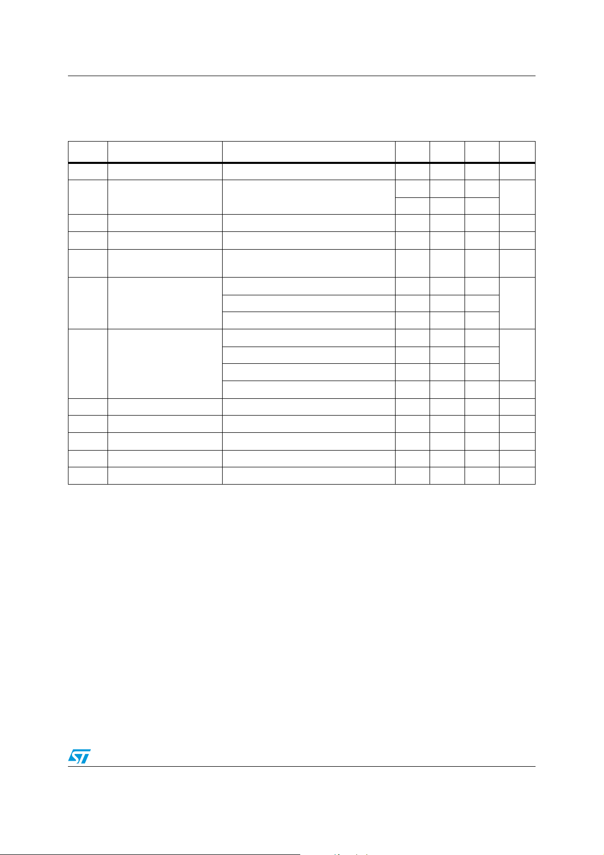
LD29080xx Electrical characteristics
IO = 10 mA, (
Note 4
) TJ = 25 °C, VI = 3.5 V, V
= 2 V, CI = 330 nF, CO = 10 µF, unless
INH
otherwise specified.
Table 6. Electrical characteristics of LD29080#18
Symbol Parameter Test conditions Min. Typ. Max. Unit
V
I
V
O
ΔV
O
ΔV
O
SVR Supply voltage rejection
V
DROP
I
q
I
sc
V
IL
V
IH
I
INH
eN Output noise voltage B
Operating input voltage IO = 10mA to 800mA 2.5 13 V
Output voltage
IO = 10mA to 800mA, VI = 3 to 7.3V
T
= -40 to 125°C
J
1.782 1.8 1.818
1.755 1.845
Load regulation IO = 10mA to 800mA 0.2 1.0 %
Line regulation VI = 3 to 13V 0.06 0.5 %
Dropout voltage
f = 120 Hz, VI = 3.8 ± 1V, IO = 400mA
Note 1
)
(
IO = 150mA, TJ = -40 to 125°C (
Note 2
Note 2
I
= 800mA, TJ = -40 to 125°C (
O
I
= 10mA, TJ = -40 to 125°C 2 5
O
Note 2
62 72 dB
)0.1
)0.2
)0.40.7
mAIO = 400mA, TJ = -40 to 125°C 8 20
Quiescent current
I
= 800mA, TJ = -40 to 125°C 14 35
O
V
= 13V, V
I
= GND, TJ = -40 to 125°C 130 180 µA
INH
Short circuit current RL = 0 1.2 A
Control input logic low OFF MODE, TJ = -40 to 125°C 0.8 V
Control input logic high ON MODE, TJ = -40 to 125°C 2 V
Control input current V
= 13V, TJ = -40 to 125°C 5 10 µA
INH
= 10Hz to 100kHz, IO = 100mA 72 µV
P
V
VIO = 400mA, TJ = -40 to 125°C (
RMS
Note: 1 Guaranteed by design.
2 Dropout voltage is defined as the input-to-output differential when the output voltage drops
to 99% of its nominal value with V
3 Reference voltage is measured between output and GND pins, with ADJ PIN tied to V
4 In order to avoid any output voltage rise within the whole operating temperature range, due
to output leakage current, a minimum load current of 2 mA is required.
+ 1 V applied to VI.
O
.
O
Doc ID 10918 Rev 7 7/24
Page 8
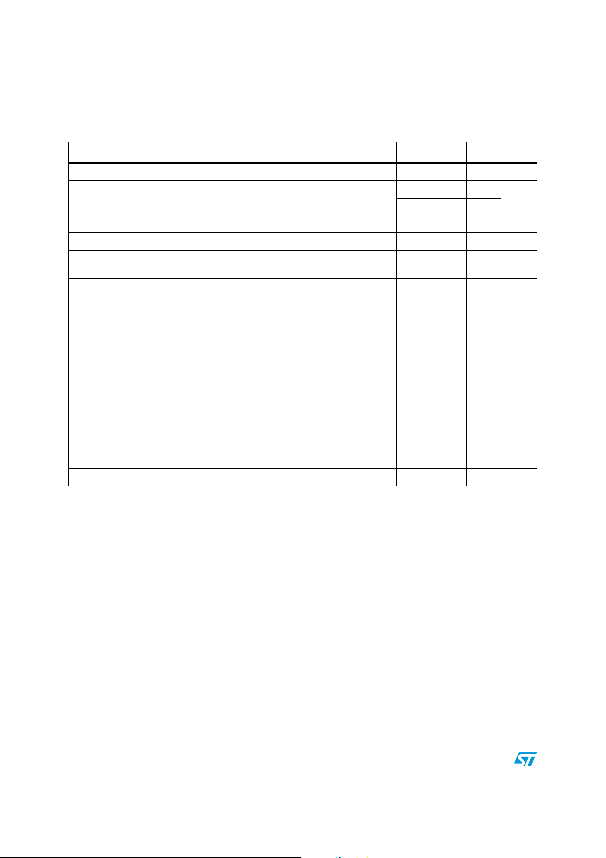
Electrical characteristics LD29080xx
IO = 10 mA, (
Note 4
) TJ = 25 °C, VI = 4.5 V, V
= 2 V, CI = 330 nF, CO = 10 µF, unless
INH
otherwise specified.
Table 7. Electrical characteristics of LD29080#25
Symbol Parameter Test conditions Min. Typ. Max. Unit
V
I
V
O
ΔV
O
ΔV
O
SVR Supply voltage rejection
V
DROP
I
q
I
sc
V
IL
V
IH
I
INH
eN Output noise voltage B
Operating input voltage IO = 10mA to 800mA 13 V
Output voltage
IO = 10mA to 800mA, VI = 3.5 to 8V
T
= -40 to 125°C
J
2.475 2.5 2.525
2.438 2.562
Load regulation IO = 10mA to 800mA 0.2 1.0 %
Line regulation VI = 3.5 to 13V 0.06 0.5 %
Dropout voltage
f = 120 Hz, VI = 4.5 ± 1V, IO = 400mA
Note 1
)
(
IO = 150mA, TJ = -40 to 125°C (
Note 2
Note 2
I
= 800mA, TJ = -40 to 125°C (
O
I
= 10mA, TJ = -40 to 125°C 2 5
O
Note 2
55 70 dB
)0.1
)0.2
)0.40.7
mAIO = 400mA, TJ = -40 to 125°C 8 20
Quiescent current
I
= 800mA, TJ = -40 to 125°C 14 35
O
V
= 13V, V
I
= GND, TJ = -40 to 125°C 130 180 µA
INH
Short circuit current RL = 0 1.2 A
Control input logic low OFF MODE, TJ = -40 to 125°C 0.8 V
Control input logic high ON MODE, TJ = -40 to 125°C 2 V
Control input current V
= 13V, TJ = -40 to 125°C 5 10 µA
INH
= 10Hz to 100kHz, IO = 100mA 100 µV
P
V
VIO = 400mA, TJ = -40 to 125°C (
RMS
Note: 1 Guaranteed by design.
2 Dropout voltage is defined as the input-to-output differential when the output voltage drops
to 99% of its nominal value with V
+ 1 V applied to VI.
O
3 Reference voltage is measured between output and GND pins, with ADJ PIN tied to V
4 In order to avoid any output voltage rise within the whole operating temperature range, due
to output leakage current, a minimum load current of 2 mA is required.
8/24 Doc ID 10918 Rev 7
.
O
Page 9

LD29080xx Electrical characteristics
IO = 10 mA, (
Note 4
) TJ = 25 °C, VI = 5.3 V, V
= 2 V, CI = 330 nF, CO = 10 µF, unless
INH
otherwise specified.
Table 8. Electrical characteristics of LD29080#33
Symbol Parameter Test conditions Min. Typ. Max. Unit
V
I
V
O
ΔV
O
ΔV
O
SVR Supply voltage rejection
V
DROP
I
q
I
sc
V
IL
V
IH
I
INH
eN Output noise voltage B
Operating input voltage IO = 10mA to 800mA 13 V
Output voltage
IO = 10mA to 800mA, VI = 4.3 to 8.8V
T
= -40 to 125°C
J
3.267 3.3 3.333
3.218 3.382
Load regulation IO = 10mA to 800mA 0.2 1.0 %
Line regulation VI = 4.3 to 13V 0.06 0.5 %
Dropout voltage
f = 120 Hz, VI = 5.3 ± 1V, IO = 400mA
Note 1
)
(
IO = 150mA, TJ = -40 to 125°C (
Note 2
Note 2
I
= 800mA, TJ = -40 to 125°C (
O
I
= 10mA, TJ = -40 to 125°C 2 5
O
Note 2
52 67 dB
)0.1
)0.2
)0.40.7
mAIO = 400mA, TJ = -40 to 125°C 8 20
Quiescent current
I
= 800mA, TJ = -40 to 125°C 14 35
O
V
= 13V, V
I
= GND, TJ = -40 to 125°C 130 180 µA
INH
Short circuit current RL = 0 1.2 A
Control input logic low OFF MODE, TJ = -40 to 125°C 0.8 V
Control input logic high ON MODE, TJ = -40 to 125°C 2 V
Control input current V
= 13V, TJ = -40 to 125°C 5 10 µA
INH
= 10Hz to 100kHz, IO = 100mA 132 µV
P
V
VIO = 400mA, TJ = -40 to 125°C (
RMS
Note: 1 Guaranteed by design.
2 Dropout voltage is defined as the input-to-output differential when the output voltage drops
to 99% of its nominal value with V
3 Reference voltage is measured between output and GND pins, with ADJ PIN tied to V
4 In order to avoid any output voltage rise within the whole operating temperature range, due
to output leakage current, a minimum load current of 2 mA is required.
+ 1 V applied to VI.
O
.
O
Doc ID 10918 Rev 7 9/24
Page 10

Electrical characteristics LD29080xx
IO = 10 mA, (
Note 4
) TJ = 25 °C, VI = 7 V, V
= 2 V, CI = 330 nF, CO = 10 µF, unless
INH
otherwise specified.
Table 9. Electrical characteristics of LD29080#50
Symbol Parameter Test conditions Min. Typ. Max. Unit
V
I
V
O
ΔV
O
ΔV
O
SVR Supply voltage rejection
V
DROP
I
q
I
sc
V
IL
V
IH
I
INH
eN Output noise voltage B
Operating input voltage IO = 10mA to 800mA 13 V
Output voltage
IO = 10mA to 800mA, VI = 6 to 10.5V
T
= -40 to 125°C
J
4.9555.05
4.875 5.125
Load regulation IO = 10mA to 800mA 0.2 1.0 %
Line regulation VI = 6 to 13V 0.06 0.5 %
Dropout voltage
f = 120 Hz, VI = 7 ± 1V, IO = 400mA
Note 1
)
(
IO = 150mA, TJ = -40 to 125°C (
Note 2
Note 2
I
= 800mA, TJ = -40 to 125°C (
O
I
= 10mA, TJ = -40 to 125°C 2 5
O
Note 2
49 64 dB
)0.1
)0.2
)0.40.7
mAIO = 400mA, TJ = -40 to 125°C 8 20
Quiescent current
I
= 800mA, TJ = -40 to 125°C 14 35
O
V
= 13V, V
I
= GND, TJ = -40 to 125°C 130 180 µA
INH
Short circuit current RL = 0 1.2 A
Control input logic low OFF MODE, TJ = -40 to 125°C 0.8 V
Control input logic high ON MODE, TJ = -40 to 125°C 2 V
Control input current V
= 13V, TJ = -40 to 125°C 5 10 µA
INH
= 10Hz to 100kHz, IO = 100mA 180 µV
P
V
VIO = 400mA, TJ = -40 to 125°C (
RMS
Note: 1 Guaranteed by design.
2 Dropout voltage is defined as the input-to-output differential when the output voltage drops
to 99% of its nominal value with V
+ 1 V applied to VI.
O
3 Reference voltage is measured between output and GND pins, with ADJ PIN tied to V
4 In order to avoid any output voltage rise within the whole operating temperature range, due
to output leakage current, a minimum load current of 2 mA is required.
10/24 Doc ID 10918 Rev 7
.
O
Page 11

LD29080xx Electrical characteristics
IO = 10 mA, (
Note 4
) TJ = 25 °C, VI = 10 V, V
= 2 V, CI = 330 nF, CO = 10 µF, unless
INH
otherwise specified)
Table 10. Electrical characteristics of LD29080#80
Symbol Parameter Test conditions Min. Typ. Max. Unit
V
I
V
O
ΔV
O
ΔV
O
SVR Supply voltage rejection
V
DROP
I
q
I
sc
V
IL
V
IH
I
INH
eN Output noise voltage B
Operating input voltage IO = 10mA to 800mA 13 V
Output voltage
IO = 10mA to 800mA, VI = 9 to 13V
T
= -40 to 125°C
J
7.9288.08
7.80 8.20
Load regulation IO = 10mA to 800mA 0.2 1.0 %
Line regulation VI = 9 to 13V 0.06 0.5 %
Dropout voltage
f = 120 Hz, VI = 10 ± 1V, IO = 400mA
Note 1
)
(
IO = 150mA, TJ = -40 to 125°C (
Note 2
Note 2
I
= 800mA, TJ = -40 to 125°C (
O
I
= 10mA, TJ = -40 to 125°C 2 5
O
Note 2
45 59 dB
)0.1
)0.2
)0.40.7
mAIO = 400mA, TJ = -40 to 125°C 8 20
Quiescent current
I
= 800mA, TJ = -40 to 125°C 14 35
O
V
= 13V, V
I
= GND, TJ = -40 to 125°C 130 180 µA
INH
Short circuit current RL = 0 1.2 A
Control input logic low OFF MODE, TJ = -40 to 125°C 0.8 V
Control input logic high ON MODE, TJ = -40 to 125°C 2 V
Control input current V
= 13V, TJ = -40 to 125°C 5 10 µA
INH
= 10Hz to 100kHz, IO = 100mA 320 µV
P
V
VIO = 400mA, TJ = -40 to 125°C (
RMS
Note: 1 Guaranteed by design.
2 Dropout voltage is defined as the input-to-output differential when the output voltage drops
to 99% of its nominal value with V
3 Reference voltage is measured between output and GND pins, with ADJ PIN tied to V
4 In order to avoid any output voltage rise within the whole operating temperature range, due
to output leakage current, a minimum load current of 2 mA is required.
+ 1 V applied to VI.
O
.
O
Doc ID 10918 Rev 7 11/24
Page 12

Electrical characteristics LD29080xx
IO = 10 mA, (
Note 4
) TJ = 25 °C, VI = 11 V, V
= 2 V, CI = 330 nF, CO = 10 µF, unless
INH
otherwise specified.
Table 11. Electrical characteristics of LD29080#90
Symbol Parameter Test conditions Min. Typ. Max. Unit
V
I
V
O
ΔV
O
ΔV
O
SVR Supply voltage rejection
V
DROP
I
q
I
sc
V
IL
V
IH
I
INH
eN Output noise voltage B
Operating input voltage IO = 10mA to 800mA 13 V
Output voltage
IO = 10mA to 800mA, VI = 9 to 13V
T
= -40 to 125°C
J
8.9199.09
8.775 9.225
Load regulation IO = 10mA to 800mA 0.2 1.0 %
Line regulation VI = 10 to 13V 0.06 0.5 %
Dropout voltage
f = 120 Hz, VI = 11 ± 1V, IO = 400mA
Note 1
)
(
IO = 150mA, TJ = -40 to 125°C (
Note 2
Note 2
I
= 800mA, TJ = -40 to 125°C (
O
I
= 10mA, TJ = -40 to 125°C 2 5
O
Note 2
43 57 dB
)0.1
)0.2
)0.40.7
mAIO = 400mA, TJ = -40 to 125°C 8 20
Quiescent current
I
= 800mA, TJ = -40 to 125°C 14 35
O
V
= 13V, V
I
= GND, TJ = -40 to 125°C 130 180 µA
INH
Short circuit current RL = 0 1.2 A
Control input logic low OFF MODE, TJ = -40 to 125°C 0.8 V
Control input logic high ON MODE, TJ = -40 to 125°C 2 V
Control input current V
= 13V, TJ = -40 to 125°C 5 10 µA
INH
= 10Hz to 100kHz, IO = 100mA 330 µV
P
V
VIO = 400mA, TJ = -40 to 125°C (
RMS
Note: 1 Guaranteed by design.
2 Dropout voltage is defined as the input-to-output differential when the output voltage drops
to 99% of its nominal value with V
+ 1 V applied to VI.
O
3 Reference voltage is measured between output and GND pins, with ADJ PIN tied to V
4 In order to avoid any output voltage rise within the whole operating temperature range, due
to output leakage current, a minimum load current of 2 mA is required.
12/24 Doc ID 10918 Rev 7
.
O
Page 13

LD29080xx Electrical characteristics
IO = 10 mA, (
Note 4
) TJ = 25 °C, VI = 10 V, V
= 2 V, CI = 330 nF, CO = 10 µF, unless
INH
otherwise specified.
Table 12. Electrical characteristics of LD29080#ADJ
Symbol Parameter Test conditions Min. Typ. Max. Unit
V
I
ΔV
O
ΔVOLine regulation VI = 2.5 to 13V, IO = 10mA 0.06 0.5 %
V
REF
SVR Supply voltage rejection
I
q
I
ADJ
I
sc
V
IL
V
IH
I
INH
eN Output noise voltage B
Operating input voltage IO = 10mA to 800mA 2.5 13 V
Load regulation IO = 10mA to 800mA 0.2 1.0 %
Reference voltage
= 10mA to 800mA, VI = 2.5 to 6.73V
I
O
= -40 to 125°C (
T
J
f = 120 Hz, V
Note 1
)
(
I
= 10mA, TJ = -40 to 125°C 2 5
O
Note 3
)
= 3.23 ± 1V, IO = 400mA
I
1.2177 1.23 1.2423
1.1993 1.2607
45 75 dB
mAIO = 400mA, TJ = -40 to 125°C 8 20
Quiescent current
I
= 800mA, TJ = -40 to 125°C 14 35
O
V
= 13V, V
I
= GND, TJ = -40 to 125°C 130 180 µA
INH
Adjust pin current TJ = -40 to 125°C 1 µA
Short circuit current RL = 0 1.2 A
Control input logic low OFF MODE, TJ = -40 to 125°C 0.8 V
Control input logic high ON MODE, TJ = -40 to 125°C 2 V
Control input current V
= 13V, TJ = -40 to 125°C 5 10 µA
INH
= 10Hz to 100kHz, IO = 100mA 50 µV
P
V
RMS
Note: 1 Guaranteed by design.
2 Dropout voltage is defined as the input-to-output differential when the output voltage drops
to 99% of its nominal value with V
3 Reference voltage is measured between output and GND pins, with ADJ PIN tied to V
4 In order to avoid any output voltage rise within the whole operating temperature range, due
to output leakage current, a minimum load current of 2 mA is required.
+ 1 V applied to VI.
O
.
O
Doc ID 10918 Rev 7 13/24
Page 14

Typical characteristics LD29080xx
5 Typical characteristics
Figure 5. Output voltage vs. temperature Figure 6. Reference voltage vs. temperature
Figure 7. Dropout voltage vs. temperature Figure 8. Dropout voltage vs. output current
Figure 9. Quiescent current vs. output
current
Figure 10. Quiescent current vs. temperature
14/24 Doc ID 10918 Rev 7
(V
= 3 V)
I
Page 15

LD29080xx Typical characteristics
Figure 11. Quiescent current vs. supply
voltage
Figure 13. Short circuit current vs.
temperature
Figure 12. Quiescent current vs. temperature
(V
= 3.5 V)
I
Figure 14. Adjust pin current vs. temperature
Figure 15. Supply voltage rejection vs.
temperature
Doc ID 10918 Rev 7 15/24
Figure 16. Output voltage vs. input voltage
Page 16

Typical characteristics LD29080xx
Figure 17. Stability vs. C
Figure 19. Load transient
O
Figure 18. Line transient
VI = 3.5 to 13 V, IO = 10 mA, VO = 1.5 V
VI = 3.5 V, IO = 10 mA to 0.8 A, VO = 1.5 V
16/24 Doc ID 10918 Rev 7
Page 17

LD29080xx Package mechanical data
6 Package mechanical data
In order to meet environmental requirements, ST offers these devices in different grades of
ECOPACK
specifications, grade definitions and product status are available at:
ECOPACK
®
packages, depending on their level of environmental compliance. ECOPACK®
®
is an ST trademark.
www.st.com
.
Doc ID 10918 Rev 7 17/24
Page 18

Package mechanical data LD29080xx
PPAK mechanical data
Dim.
Min. Typ. Max. Min. Typ. Max.
A 2.2 2.4 0.086 0.094
A1 0.9 1.1 0.035 0.043
A2 0.03 0.23 0.001 0.009
B 0.4 0.6 0.015 0.023
B2 5.2 5.4 0.204 0.212
C 0.45 0.6 0.017 0.023
C2 0.48 0.6 0.019 0.023
D 6 6.2 0.236 0.244
D1 5.1 0.201
E 6.4 6.6 0.252 0.260
E1 4.7 0.185
e 1.27 0.050
G4.9 5.25 0.193 0.206
G1 2.38 2.7 0.093 0.106
H 9.35 10.1 0.368 0.397
L2 0.8 1 0.031
L4 0.6 1 0.023 0.039
L5 1
L6 2.8 0.110
mm. inch.
0.039
0.039
18/24 Doc ID 10918 Rev 7
0078180-E
Page 19

LD29080xx Package mechanical data
DPAK mechanical data
Dim.
Min. Typ. Max. Min. Typ. Max.
A 2.2 2.4 0.086 0.094
A1 0.9 1.1 0.035 0.043
A2 0.03 0.23 0.001 0.009
B 0.64 0.9 0.025 0.035
b4 5.2 5.4 0.204 0.212
C 0.45 0.6 0.017 0.023
C2 0.48 0.6 0.019 0.023
D 6 6.2 0.236 0.244
D1 5.1 0.200
E 6.4 6.6 0.252 0.260
E1 4.7 0.185
e2.28 0.090
e1 4.4 4.6 0.173 0.181
H 9.35 10.1 0.368 0.397
L 1 0.039
(L1)
L2 0.8 0.031
L4 0.6 1 0.023 0.039
R 0.2 0.008
V2 0° 8°0° 8°
mm. inch.
2.8 0.110
0068772-F
Doc ID 10918 Rev 7 19/24
Page 20

Package mechanical data LD29080xx
SOT223 mechanical data
mm. mils.
Dim.
Min. Typ. Max. Min. Typ. Max.
A1.8 70.9
A1 0.02 0.1 0.83.9
B 0.6 0.7 0.8523.6 27.6 33.5
B1 2.933.15 114.2 118.1 124.0
c 0.24 0.26 0.35 9.4 10.2 13.8
D6.3 6.5 6.7 248.0 255.9 263.8
e2.390.6
e1 4.6 181.1
E 3.33.5 3.7 129.9 137.8 145.7
H6.7 7 7.3 263.8 275.7 287.5
V 10° 10°
20/24 Doc ID 10918 Rev 7
0046067/H
Page 21

LD29080xx Package mechanical data
Tape & reel DPAK-PPAK mechanical data
Dim.
Min. Typ. Max. Min. Typ. Max.
A 330 12.992
C12.8 13.0 13.2 0.504 0.512 0.519
D 20.2 0.795
N60 2.362
T22.40.882
Ao 6.806.90 7.00 0.268 0.272 0.2.76
Bo 10.40 10.50 10.60 0.409 0.413 0.417
Ko 2.55 2.65 2.75 0.100 0.104 0.105
Po 3.9 4.0 4.1 0.153 0.157 0.161
P7.98.0 8.1 0.311 0.315 0.319
mm. inch.
Doc ID 10918 Rev 7 21/24
Page 22

Package mechanical data LD29080xx
Tape & reel SOT223 mechanical data
Dim.
Min. Typ. Max. Min. Typ. Max.
A 330 12.992
C 12.8 13.0 13.2 0.504 0.512 0.519
D 20.2 0.795
N60 2.362
T 14.4 0.567
Ao 6.73 6.83 6.93 0.265 0.269 0.273
Bo 7.32 7.42 7.52 0.288 0.292 0.296
Ko 1.78 2 0.070 0.078
Po 3.9 4.0 4.1 0.153 0.157 0.161
P7.98.0 8.1 0.311 0.315 0.319
mm. inch.
22/24 Doc ID 10918 Rev 7
Page 23

LD29080xx Revision history
7 Revision history
Table 13. Document revision history
Date Revision Changes
15-Oct-2004 1 First release.
20-Oct-2005 2 Order codes updated.
14-May-2007 3 Order codes updated.
26-Jan-2009 4 Modified: eN value in
22-Feb-2011 5 Added: new order code
12-Jan-2012 6 Modified: R
thJA
Table 9 on page 10
Table 1 on page 1
and R
thJC
.
and mechanical data.
value for SOT223
Table 4 on page 5
08-May-2012 7 Modified: pin connections for PPAK, DPAK and SOT223
.
Figure 3 on page 4
.
Doc ID 10918 Rev 7 23/24
Page 24

LD29080xx
Please Read Carefully:
Information in this document is provided solely in connection with ST products. STMicroelectronics NV and its subsidiaries (“ST”) reserve the
right to make changes, corrections, modifications or improvements, to this document, and the products and services described herein at any
time, without notice.
All ST products are sold pursuant to ST’s terms and conditions of sale.
Purchasers are solely responsible for the choice, selection and use of the ST products and services described herein, and ST assumes no
liability whatsoever relating to the choice, selection or use of the ST products and services described herein.
No license, express or implied, by estoppel or otherwise, to any intellectual property rights is granted under this document. If any part of this
document refers to any third party products or services it shall not be deemed a license grant by ST for the use of such third party products
or services, or any intellectual property contained therein or considered as a warranty covering the use in any manner whatsoever of such
third party products or services or any intellectual property contained therein.
UNLESS OTHERWISE SET FORTH IN ST’S TERMS AND CONDITIONS OF SALE ST DISCLAIMS ANY EXPRESS OR IMPLIED
WARRANTY WITH RESPECT TO THE USE AND/OR SALE OF ST PRODUCTS INCLUDING WITHOUT LIMITATION IMPLIED
WARRANTIES OF MERCHANTABILITY, FITNESS FOR A PARTICULAR PURPOSE (AND THEIR EQUIVALENTS UNDER THE LAWS
OF ANY JURISDICTION), OR INFRINGEMENT OF ANY PATENT, COPYRIGHT OR OTHER INTELLECTUAL PROPERTY RIGHT.
UNLESS EXPRESSLY APPROVED IN WRITING BY TWO AUTHORIZED ST REPRESENTATIVES, ST PRODUCTS ARE NOT
RECOMMENDED, AUTHORIZED OR WARRANTED FOR USE IN MILITARY, AIR CRAFT, SPACE, LIFE SAVING, OR LIFE SUSTAINING
APPLICATIONS, NOR IN PRODUCTS OR SYSTEMS WHERE FAILURE OR MALFUNCTION MAY RESULT IN PERSONAL INJURY,
DEATH, OR SEVERE PROPERTY OR ENVIRONMENTAL DAMAGE. ST PRODUCTS WHICH ARE NOT SPECIFIED AS "AUTOMOTIVE
GRADE" MAY ONLY BE USED IN AUTOMOTIVE APPLICATIONS AT USER’S OWN RISK.
Resale of ST products with provisions different from the statements and/or technical features set forth in this document shall immediately void
any warranty granted by ST for the ST product or service described herein and shall not create or extend in any manner whatsoever, any
liability of ST.
ST and the ST logo are trademarks or registered trademarks of ST in various countries.
Information in this document supersedes and replaces all information previously supplied.
The ST logo is a registered trademark of STMicroelectronics. All other names are the property of their respective owners.
© 2012 STMicroelectronics - All rights reserved
STMicroelectronics group of companies
Australia - Belgium - Brazil - Canada - China - Czech Republic - Finland - France - Germany - Hong Kong - India - Israel - Italy - Japan -
Malaysia - Malta - Morocco - Philippines - Singapore - Spain - Sweden - Switzerland - United Kingdom - United States of America
www.st.com
24/24 Doc ID 10918 Rev 7
 Loading...