

Page 1
Overview
The LC89210 is a highly integrated modem engine that
can be used in products that support transmission rates up
to the 14,400 bps rate used in contemporary group III fax
equipment. The LC89210 is compatible with V.21, V.23
and Bell 103 full-duplex modems.
Features
• Supports the ITU-T V.17, V.29, and V.27ter fax
standards
• ITU-T V.23, V.21, and Bell 103
• V.17, V.29 (T104), and V.27ter short training
• V.33 half duplex
• 1800-Hz or 1700-Hz carrier
• The LC89210 is a complete data pump on a single chip.
• 5 V single-voltage power supply
— Operating power dissipation: 375 mW (typical)
— Low power mode: 5 mW (typical)
• Expanded operating modes
— Full implementation of V.17, V.33, V.29, and
V.27ter handshaking
— Autodial and autoanswer functions
— Programmable tone detection and FSK V.21 flag
pattern detection during high-speed reception
— Programmable call progresss and call waiting tone
detection, including DTMF
— Support for programmable CLASSTMdetection
— Wide dynamic range (better than 48 dB)
— A-law voice PCM mode
• Multiple interfaces
— Parallel 64 ×8-bit dual-port RAM
— Synchronous/HDLC parallel data processing
— Support for HDLC framing
— V.24 interface
— Can monitor all operating states in real time.
— Includes all diagnostic functions.
— Dual 8-bit D/A converter for eye pattern display
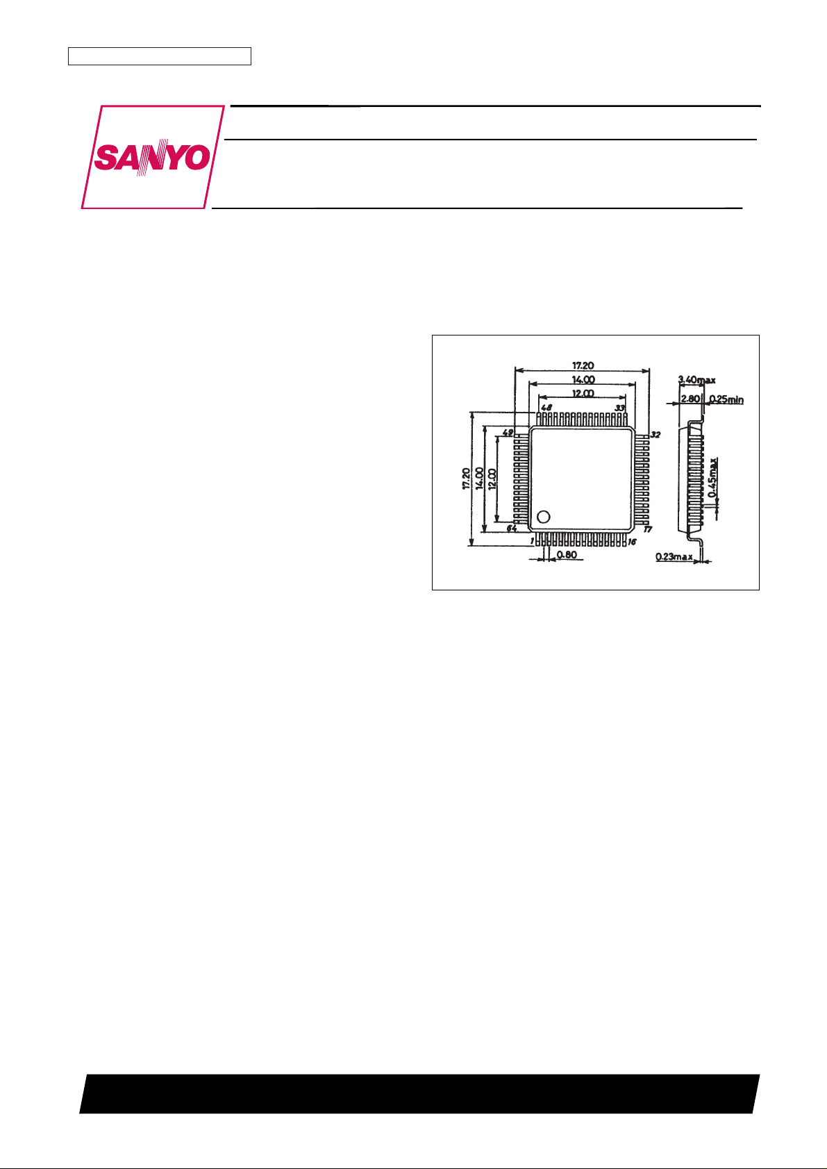
Package Dimensions
unit: mm
3213-PQFP64
CMOS LSI
52696HA (OT) No. 5382-1/10
Preliminaly
SANYO: PQFP64
[LC89210]
SANYO Electric Co.,Ltd. Semiconductor Bussiness Headquarters
TOKYO OFFICE Tokyo Bldg., 1-10, 1 Chome, Ueno, Taito-ku, TOKYO, 110 JAPAN
High-speed fax modem data pump
LC89210
Ordering number : EN*5382
Page 2
No. 5382-2/10
LC89210
Specifications
Electrical Specifications at Ta = 25°C, VDD= 5 V (unless otherwise specified)
Absolute Maximum Ratings with respect to ground
Electrical Characteristics at Ta = 0 to +70°C, VDD= 5.0 V ± 5%, GND = 0 V (unless otherwise specified)
Parameter Symbol Conditions Ratings Unit
DC supply voltage V
DD
–0.3 to +7.0 V
Digital or analog input voltage V
I
, V
IN
–0.3 to (VDD+ 0.3) V
Digital or analog input current I
I
, I
IN
±1 mA
Digital output current I
O
±20 mA
Analog output current I
OUT
±10 mA
Allowable power dissipation Pd max 1000 mW
Operating temperature Topr 0 to +70 °C
Storage temperature (plastic) Tstg –40 to +125 °C
Parameter Symbol Conditions min typ max Unit
[Power Supply and Common-Mode Voltages]
Supply voltage V
DD
4.75 5 5.25 V
Current drain I
DD
75 100 mA
Current drain in lower power mode I
DD-ip
1 mA
Common-mode voltage V
CM
VDD/2 – 5% VDD/2 VDD/2 + 5% V
[Crystal Oscillator Interface] XTAL and EXTAL
Input low-level voltage V
IL
1.5 V
Input high-level voltage V
IH
3.5 V
Input low-level current I
L
GND < VI< VILmax –15 µA
Input high-level current I
H
VIHmin < VI< V
DD
15 µA
[Digital Interface] All digital pins except the XTAL pin
Input low-level voltage V
IL
–0.3 +0.8 V
Input high-level voltage V
IH
2.2 V
Input current I
I
VI= VDDor VI= GND –10 0 +10 µA
Output high-level voltage V
OHIlord
= 2 mA 2.4 V
Output low-level voltage V
OL
I
lord
= 2 mA 0.4 V
3-state input leakage current I
OZ
GND < VO< V
DD
–50 0 +50 µA
Input capacitance C
IN
5 pF
[Analog Interface]
Differential reference voltage input V
REF
V
REFP
– V
REFN
2.40 2.50 2.60 V
Input common-mode offset V
CMOin
V = (RXA1 + RXA2)/2 – V
CM
–300 +300 mV
Differential input voltage V
DIFin
RXA1 – RXA2 2 × V
REF
Vp-p
Output common-mode
V
CMOout
(TXA1 + TXA2)/2 – V
CM
–200 +200 mV
voltage offset
Differential output voltage V
DIFout
TXA1 – TXA2 2 × V
REF
Vp-p
Differential output DC offset V
OFFout
(TXA1 – TXA2) –100 +100 mV
Input resistance Rin RXA
X
100 kΩ
Output resistance Rout TXA
X
20 Ω
Load resistance R
L
TXA
X
10 kΩ
Load capacitance C
L
TXA
X
50 pF
Page 3
No. 5382-3/10
LC89210
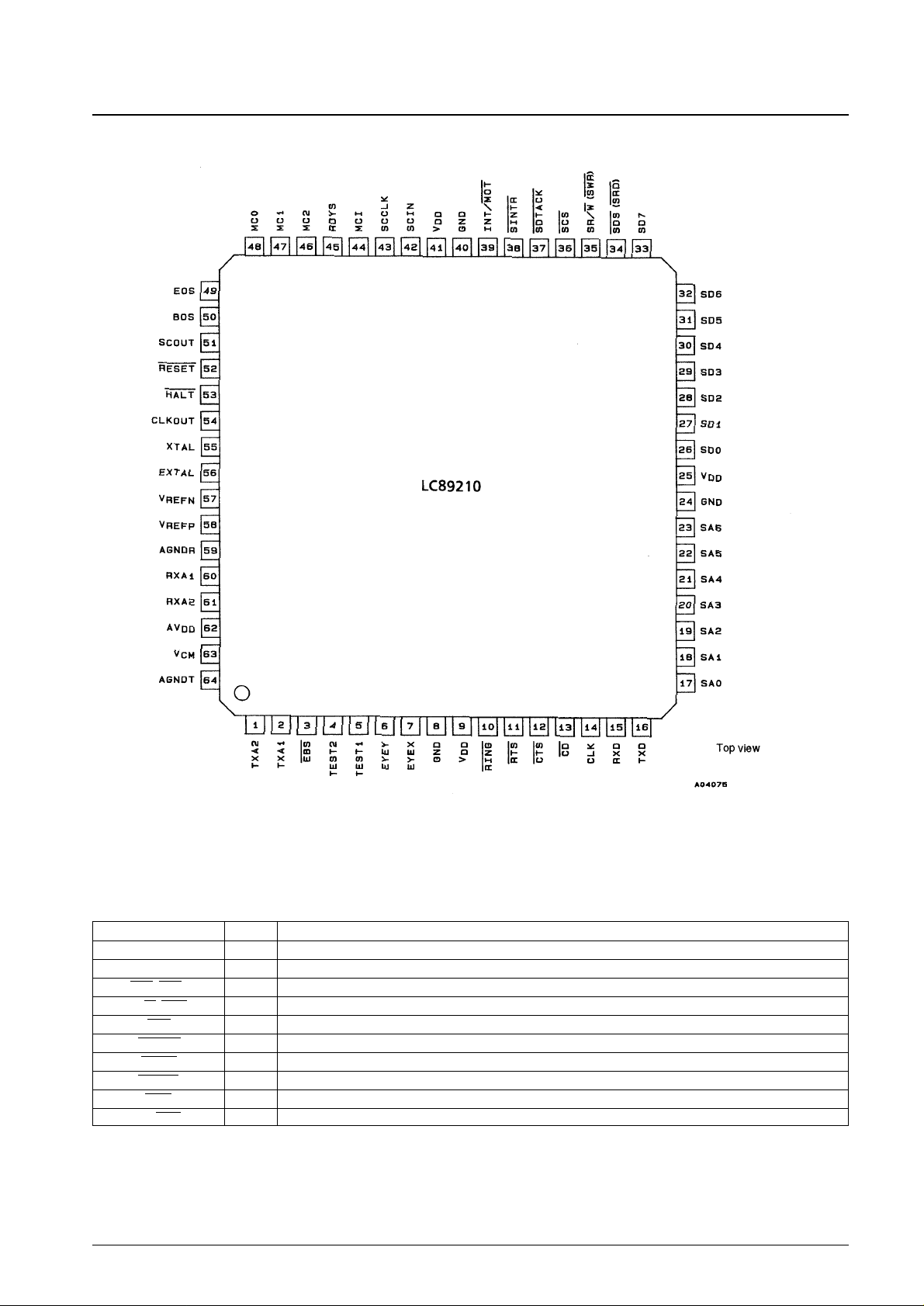
Pin Assignment
Host Interface
The LC89210 is interfaced to the control processor through a 64-byte dual-port RAM that is shared by the LC89210 and
the host.
Note: * Open-drain output
Pin Type Function
SD0 to SD7 I/O System data bus
SA0 to SA6 I System address bus
SDS (SDR) I System data strobe
SR/W (SWR) I System read/write
SCS I System chip select
SDTACK OD* System bus data acknowledge
SINTR OD* System interrupt request
RESET I Reset. This is an active-low signal.
RING I Ring detect signal
INT/MOT I Intel/Motorola interface
Page 4

No. 5382-4/10
LC89210
Analog Interface
V.24 Interface
Other Interfaces
Note: The LC89210 nominal external clock frequency is 29.4912 MHz. This value has a precision of ±5.10–5.
Boundary Scan Interface
The LC89210 provides 13 signals for testing. These signals can be used along with the SGS-Thomson ST18932
boundary scan development tools in the product development process to debug application hardware and software. If this
function is not used, all of these input signal must be connected to ground, and all of these output signals must be left
open.
Pin Type Function
TXA1 O Transmission analog output 1
TXA2 O Transmission analog output 2
RXA1 I Reception analog input 1
RXA2 I Reception analog input 2
V
CM
I/O Analog common voltage (nominal value: +2.5 V)
V
REFN
I Analog negative reference voltage (nominal value: CM – 1.25 V)
V
REFP
I Analog positive reference voltage (nominal value: CM + 1.25 V)
Pin Type Function
RTS I Transfer request. This is an active-low signal.
CLK O Data bit clock
CTS O Clear to send. This is an active-low signal.
RXD O Reception data
TXD I Transfer data
CD O Carrier detect. This is an active-low signal.
Pin Type Function
XTAL O Internal oscillator output
EXTAL I Internal oscillator input or external clock
EYEX O Constellation X analog coordinate (eye pattern)
EYEY O Constellation Y analog coordinate (eye pattern)
TEST1 This pin must be left open
TEST2 This pin must be left open
Pin Type Function
SCIN I Scan data input
SCCLK I Scan clock
SCOUT O Scan data output
BOS I Scan control start
EOS I Scan stop
MC0 to MC2 I Mode control
HALT I LC89210 execution step
MC1 O Multi-cycle instruction
RDYS O Scan flag ready
EBS I Enable boundary scan
CLKOUT O LC89210 internal clock (the crystal oscillator frequency divided by 2)
Page 5

No. 5382-5/10
LC89210
Power Supply
Block Diagrams
Function Block Diagram
Hardware Block Diagram
Symbol Parameter
V
DD
Digital +5 V (pins 9, 25, and 41)
GND Digital ground (pins 8, 24, and 40)
AV
DD
Analog +5 V (pin 62)
AGNDT Analog transmission system ground (pin 64)
AGNDR Analog reception system ground (pin 59)
Page 6

No. 5382-6/10
LC89210
AC Electrical Characteristics
Dual-Port RAM Host Timing
Note: * The minimum delay of 70 ns is the time from the rising edge of NWRITE to the next falling edge on either NREAD or NWRITE.
Parameter Number Conditions min typ max Unit
Address and control setup time 1 5 ns
SDTACK acknowledge 2 20 ns
Data setup time 3 10 ns
Address and control hold time 4 0 ns
Data hold time 5 5 ns
SDTACK hold time 6 0 ns
Write enable low state 7 45 ns
Access inhibition high state 8 70* ns
Read enable low state 9 45 ns
Read data access 10 35 ns
SINTR clear delay 11 50 ns
Data valid to tristate 12 15 ns
Page 7

No. 5382-7/10
LC89210
Serial V.24 Interface Timing
Parameter Number Conditions min typ max Unit
TXD to CLK setup time 1 30 ns
TXD to CLK hold time 2 10 ns
RXD valid to CLK delay time 3 100 ns
RXD valid to CLK hold time 4 0 ns
Page 8

No. 5382-8/10
LC89210
Electrical Circuit Diagrams
Oscillator
We recommend the use of the following circuit if an overtone crystal oscillator is used in series resonance mode.
Page 9

No. 5382-9/10
LC89210
Printed Circuit Board Design Guidelines
While the two most important factors influencing the performance of this fax modem are the performance of the
LC89210 itself and the appropriateness of the design of the printed circuit board, it is not the purpose of this section to
describe all aspects of modem printed circuit board design. Rather, this section presents the following few
recommendations.
1. 4-layer boards
The digital and analog system grounds should be separated and then connected at a single point (single-point
ground). Furthermore, the location of the single-point ground should be as close to the LC89210 as is possible.
AGNDR and AGNDT should be connected to the single-point ground location with an extremely low impedance.
2. 2-layer boards
Supply the ground grid to all empty spaces and the inner side of component spaces.
3. The 2.2 nF capacitors connected to the RXA1 and RXA2 pins should be located as close to the pins as possible.
4. The two 100 nF capacitors connected to the V
REFP
and V
REFN
pins should be located as close to the pins as possible.
5. To prevent latchup due to differences in power on timing between the analog and digital power supplies, insert two
diodes with reverse polarities in parallel between the VDD(digital) and AVDD(analog) power supplies.
Application Example
Note: The capacitors marked with asterisks (*) must be connected as close as possible to the LC89210 pins.
Signal names ending in “I” are active low signals.
If it is necessary to supply current to V
CM
, add the resistors R3, R4, R5, and R6.
Page 10

No. 5382-10/10
LC89210
This catalog provides information as of December, 1997. Specifications and information herein are subject to
change without notice.
■ No products described or contained herein are intended for use in surgical implants, life-support systems, aerospace
equipment, nuclear power control systems, vehicles, disaster/crime-prevention equipment and the like, the failure of
which may directly or indirectly cause injury, death or property loss.
■ Anyone purchasing any products described or contained herein for an above-mentioned use shall:
➀ Accept full responsibility and indemnify and defend SANYO ELECTRIC CO., LTD., its affiliates, subsidiaries and
distributors and all their officers and employees, jointly and severally, against any and all claims and litigation and all
damages, cost and expenses associated with such use:
➁ Not impose any responsibility for any fault or negligence which may be cited in any such claim or litigation on
SANYO ELECTRIC CO., LTD., its affiliates, subsidiaries and distributors or any of their officers and employees
jointly or severally.
■ Information (including circuit diagrams and circuit parameters) herein is for example only; it is not guaranteed for
volume production. SANYO believes information herein is accurate and reliable, but no guarantees are made or implied
regarding its use or any infringements of intellectual property rights or other rights of third parties.
 Loading...