

Page 1
Overview
The LC89170M is an IC that decodes the text data, such
as song names, stored in subcode channels R to W of a
compact disk’s read-in area.
Features
• Accepts the channel R to W subcode data through a
subcode interface.
• Can continuously output the channel R to W data for
each 1PACK24 symbol.
• Performs error detection (cyclic redundancy code) and
outputs both the data and the result of that check.
• Provides synchronization protection for the subcode
interface.
• Supports low-voltage operation (3.3 V)
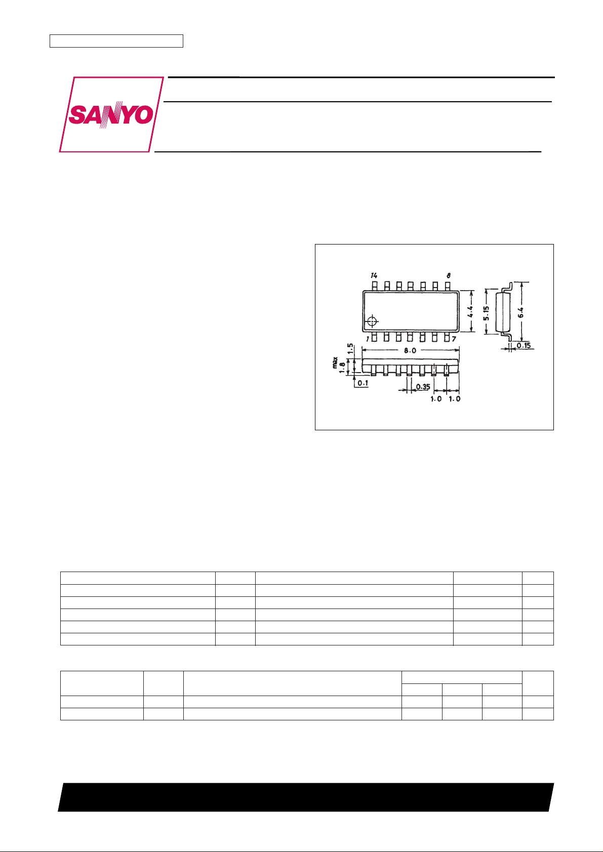
• Provided in the miniature MFP-14S package.
Package Dimensions
unit: mm
3111-MFP14S
CMOS LSI
Ordering number : EN*5536A
93096HA (OT) No. 5536-1/8
Preliminary
SANYO: MFP14S
[LC89170M]
SANYO Electric Co.,Ltd. Semiconductor Bussiness Headquarters
TOKYO OFFICE Tokyo Bldg., 1-10, 1 Chome, Ueno, Taito-ku, TOKYO, 110 JAPAN
CD Player Text Data IC
LC89170M
Specifications
Absolute Maximum Ratings at Ta = 25 °C, VSS= 0 V
Parameter Symbol Conditions Ratings Unit
Maximum supply voltage V
DD
max –0.3 to +7.0 V
I/O voltages V
IVO
–0.3 to VDD+ 0.3 V
Input current I
I
±10 mA
Operating temperature Topr –30 to +70 °C
Storage temperature Tstg –55 to +125 °C
Recommended Operating Conditions at Ta = 25 °C, VSS= 0 V
Parameter Symbol Conditions
Ratings
Unit
min typ max
Supply voltage V
DD
3.0 5.0 5.5 V
Operating temperature Topr –30 +70 V
Page 2

Block Diagram
Pin Assignment
Pin Functions
No. 5536-2/8
LC89170M
Pin no. Symbol I/O Function
1 EXCK I/O Subcode interface shift clock input and output
2 SBSO I Subcode interface data input
3 SCOR I Subcode interface block synchronization input
4 WFCK I Subcode interface frame synchronization input
5 MCK I Clock input (16.9344 MHz)
6 XMODE I System reset and low power mode
7 GND Ground
8 TEST I Test pin (Must be connected to ground in normal operation.)
9 SW1 I EXCK I/O setting (L: clock output, H: clock input)
10 SW2 I EXCK clock output pulse width selection (L: double speed support, H: normal speed)
11 SCLK I Command interface shift clock input
12 SRDT O Command interface data output
13 DQSY O Command interface readout enable output
14 V
DD
Power supply
Page 3

No. 5536-3/8
LC89170M
DC Characteristics
DC Characteristics (1) at Ta = –30 to +70°C, VDD= 4.5 to 5.5 V, VSS= 0 V
Note: 1. The MCK, TEST, SW1, and SW2 pins
2. The EXCK, SBSO, SCOR, WFCK, XMODE, and SCLK pins
3. The EXCK, SRDT, and DQSY pins
Parameter Symbol Conditions
Ratings
Unit
min typ max
Input high-level voltage V
IH
CMOS compatible; 1* 0.7 V
DD
V
CMOS compatible Schmitt; 2* 0.8 V
DD
V
Input low-level voltage V
IL
CMOS compatible; 1* 0.3 V
DD
V
CMOS compatible Schmitt; 2* 0.2 V
DD
V
Output high-level voltage V
OHIOH
= –2 mA; 3* VDD–2.1 V
Output low-level voltage V
OLIOH
= 2 mA; 3* 0.4 V
Current drain I
DD
VDD= 5 V, Ta = 25°C, MCK = 16.93 MHz 0.8 1.6 mA
V
DD
= 5 V, XMODE = [L] 60 120 µA
AC Characteristics
• The MCK pin
AC Characteristics (1) at Ta = –30 to +70°C, VDD= 3.0 to 5.5 V, VSS= 0 V
Parameter Symbol Conditions
Ratings
Unit
min typ max
High-level pulse width t
WH
25 56 ns
Low-level pulse width t
WL
25 56 ns
Pulse period t
C
58 100 ns
Rise and fall times t
R
, t
F
12 ns
DC Characteristics (2) at Ta = –30 to +70°C, VDD= 3.0 to 3.6 V, VSS= 0 V
Note: 1. The MCK, TEST, SW1, and SW2 pins
2. The EXCK, SBSO, SCOR, WFCK, XMODE, and SCLK pins
3. The EXCK, SRDT, and DQSY pins
Parameter Symbol Conditions
Ratings
Unit
min typ max
Input high-level voltage V
IH
CMOS compatible; 1* 0.7 V
DD
V
CMOS compatible Schmitt; 2* 0.75 V
DD
V
Input low-level voltage V
IL
CMOS compatible; 1* 0.2 V
DD
V
CMOS compatible Schmitt; 2* 0.15 V
DD
V
Output high-level voltage V
OHIOH
= –1 mA; 3* VDD–0.8 V
Output low-level voltage V
OLIOH
= 1 mA; 3* 0.4 V
Current drain I
DD
VDD= 3.3 V, Ta = 25°C, MCK = 16.93 MHz 0.5 1.0 mA
V
DD
= 3.3 V, XMODE = [L] 25 50 µA
Page 4

No. 5536-4/8
LC89170M
• The SCOR and WFCK pins
AC Characteristics (2) at Ta = –30 to +70°C, VDD= 3.0 to 5.5 V
Parameter Symbol Conditions
Ratings
Unit
min typ max
Subcode block period T
B
6.0 13.3 14.7 ms
Subcode frame period T
F
60 136 150 µs
Subcode block synchronization pulse width T
BW
60 300 µs
Subcode frame synchronization
High-level pulse width t
HW
4.0 68 µs
pulse width
Low-level pulse width t
LW
1.5 68 µs
• The EXCK and SBSO pins
AC Characteristics (3) at Ta = –30 to +70°C, VDD= 3.0 to 5.5 V
Parameter Symbol Conditions
Ratings
Unit
min typ max
High-level pulse width
t
HPW
[SW1] = [L] 0.9 6.4 µs
Synchronization clock
t
HPW
[SW1] = [H] 2 4 6 µs
pulse width
Low-level pulse width
t
LPW
[SW1] = [L] 0.9 6.4 µs
t
LPW
[SW1] = [H] 2 4 6 µs
Shift clock delay time
t
CD
[SW1] = [L] 10 32 µs
t
CD
[SW1] = [H] 0.4 µs
Shift clock rise and fall times t
RX
, t
FX
30 µs
P data access time t
PAC
3 10 µs
Data hold time t
HD
0 µs
• The SCLK, SRDT, and DQSY pins
AC Characteristics (4) at Ta = –30 to +70°C, VDD= 3.0 to 5.5 V
Parameter Symbol Conditions
Ratings
Unit
min typ max
Readout period t
CW
1.5 3.3 3.7 ms
DQSY pulse width t
W
60 136 150 µs
SCLK low-level pulse width t
WL
100 ns
SCLK high-level pulse width t
WH
100 ns
SCLK delay time t
D1
100 ns
Data delay time t
D2
50 ns
Data delay time t
D3
50 ns
Page 5

No. 5536-5/8
LC89170M
Functional Description
• Subcode interface
The LC89170M accepts subcode data from the DSP using the EXCK, SBSO, SCOR, and WFCK pins. Figure 1 shows
the timing.
SW1 sets the input or output state for the EXCK pin. This pin is provided for cases where a subcode interface shift clock
source, such as a CD-G decoder circuit, is present in the vicinity of the LC89170M. Figure 2 shows usage examples.
The SW2 is selected according to the subcode block period, TB, input to the SCOR pin.
Figure 1 Subcode Interface Timing
Figure 2 SW1 Usage Examples
SW2 Selection
SW2 Function T
B
Unit
[L] Supports up to double speed playback 6.65 ms
[H] Only supports normal-speed playback 13.3 ms
Page 6

No. 5536-6/8
LC89170M
The EXCK clock characteristics are determined by SW2 as listed in the table below.
The upper boxes assume MCK = 16.934 MHz
The lower boxes indicate the relationship with MCK (T
MCK
= 1/MCK)
EXCK Clock Selection by SW2
SW1 SW2 t
CD
t
WH
t
WL
Unit
[L] [L]
12.28 1.89 1.89 µs
208T
MCK
32T
MCK
32T
MCK
µs
[L] [H]
18.90 7.56 7.56 µs
320T
MCK
128T
MCK
128T
MCK
µs
• Microcontroller interface
The LC89170M includes a 32-word × 8-bit dual-port RAM on chip, and the 1PACK 24 symbols from subcode channels
R to W can be read out once every 3.3 ms (or once every 1.66 for double-speed playback) over the microcontroller
interface. Figure 3 shows the timing.
The 1PACK 24 symbols for the subcode R to W data (18 bytes) are entered into the dual-port RAM and input to the CRC
checking circuit. After the data for 1 PACK has all been input, a falling edge is output from the DQSY pin and the CRC
flags are output from SRDT. A high is output for the CRC flags if the check returned OK. Next, 128 bits of data are
output by inputting the SCLK clock signal. A single packet of data is output by repeating this operation four times.
Figure 3 Microcontroller Interface Output Timing
Page 7

No. 5536-7/8
LC89170M
• Synchronizing signal interpolation and protection
Although the LC89170M receives data from the DSP over the subcode interface, it is possible that due to reasons such as
defects or damage to the disk, errors may occur in the synchronization pattern (SO, SI) making the LC89170M unable to
detect that synchronization pattern, or a signal that is not a synchronizing signal (SCOR) may be recognized as a
synchronizing signal making the LC89170M unable to correctly read out the data. The LC89170M includes a
synchronizing signal interpolation and protection circuit to handle these problems. Figure 4 describes this interpolation
and protection circuit.
Although the interpolation circuit generates a synchronization signal for each packet, if the synchronizing signal is
missing, it resets on the next detected synchronizing signal and once again generates a synchronizing signal for each
packet. (1)
In the protection circuit, when a synchronizing signal is detected, if that synchronizing signal does not meet the stipulated
period (98 × WFCK) with respect to the previously detected synchronizing signal, the protection circuit has the
LC89170M ignore that detected synchronizing signal. This prevents signals that are not synchronizing signals from being
mistakenly recognized as synchronizing signals. (2)
The processing performed by these circuit is reflected in the CRC flags.
At the point marked (1) in the figure, an external SCOR that differs from the interpolated was detected, and here the
interpolation circuit is synchronized with this signal.
At the point marked (2) in the figure, an external SCOR that differs from the interpolated was detected, but this external
SCOR will be ignored and the interpolation circuit will not be re-synchronized.
• System reset and low power mode
The XMODE pin functions to reset the system and to switch to low power mode. System operation can be started
correctly by applying a high level to this pin after the power-supply voltage has risen above 4.5 V (or 3.0 V). Setting the
XMODE pin low switches the LC89170M to low power mode.
Application Circuit Example
Figure 4 Synchronizing Signal Interpolation and Protection
Page 8

No. 5536-8/8
LC89170M
This catalog provides information as of September, 1996. Specifications and information herein are subject to
change without notice.
■ No products described or contained herein are intended for use in surgical implants, life-support systems, aerospace
equipment, nuclear power control systems, vehicles, disaster/crime-prevention equipment and the like, the failure of
which may directly or indirectly cause injury, death or property loss.
■ Anyone purchasing any products described or contained herein for an above-mentioned use shall:
➀
Accept full responsibility and indemnify and defend SANYO ELECTRIC CO., LTD., its affiliates, subsidiaries and
distributors and all their officers and employees, jointly and severally, against any and all claims and litigation and all
damages, cost and expenses associated with such use:
➁
Not impose any responsibility for any fault or negligence which may be cited in any such claim or litigation on
SANYO ELECTRIC CO., LTD., its affiliates, subsidiaries and distributors or any of their officers and employees
jointly or severally.
■ Information (including circuit diagrams and circuit parameters) herein is for example only; it is not guaranteed for
volume production. SANYO believes information herein is accurate and reliable, but no guarantees are made or implied
regarding its use or any infringements of intellectual property rights or other rights of third parties.
 Loading...