

Page 1
Ordering number : EN *5428A
O3097HA (OT) No. 5428-1/6
Overview
The LC89086M is a low-power high-speed 8-bit serialparallel A/D converter fabricated in a high-speed CMOS
process.
Features
• Resolution: 8 bits (with an overflow output)
• Maximum conversion rate: 20M samples per second
• Error: Less than ±1.0 LSB
• Power supply: +5-V single-voltage power supply
• Power dissipation: 150 mW (typical)
• Analog input voltage range: VSSto V
DD
• Digital output voltage: 3 state TTL level
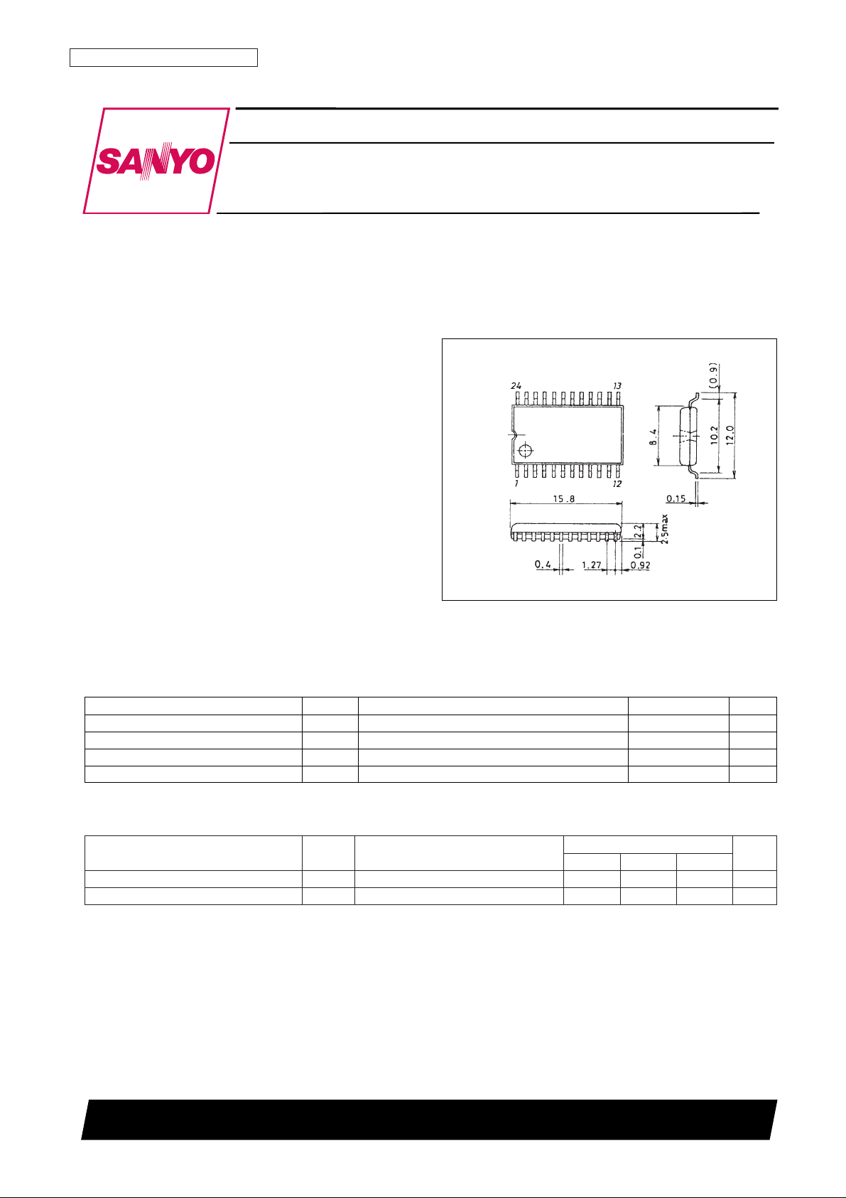
Package Dimensions
unit: mm
3155-MFP24
Preliminary
SANYO: MFP24
[LC89086M]
LC89086M
SANYO Electric Co.,Ltd. Semiconductor Bussiness Headquarters
TOKYO OFFICE Tokyo Bldg., 1-10, 1 Chome, Ueno, Taito-ku, TOKYO, 110 JAPAN
CMOS LSI
8 Bit A/D Converter
Parameter Symbol Conditions Ratings Unit
Maximum supply voltage V
DD
max –0.3 to +7.0 V
Input voltage V
IN
max –0.3 to VDD+0.3 V
Operating temperature Topr –30 to +70 °C
Storage temperature Tstg –40 to +125 °C
Specifications
Absolute Maximum Ratings at Ta = 25°C, DVSS= AV
SS
= 0 V
Parameter Symbol Conditions
Ratings
Unit
min typ max
Supply voltage V
DD
4.5 5.0 5.5 V
Operating ambient temperature Ta –30 +70
°C
Recommended Operating Conditions
Page 2
No. 5428-2/6
LC89086M
Electrical Characteristics
Electrical DC Characteristics at Ta = –30 to +70°C, AVDD= DVDD= 4.5 to 5.5 V, AVSS= DVSS= 0 V
Parameter Symbol Conditions
Ratings
Unit
min typ max
Reference resistance Rref VrefH (pin 5) – VrefL (pin 8) 210 300 390 Ω
Analog input capacitance C
AIN
30 pF
Analog input resistance R
AIN
10 MΩ
Reference high-level input voltage VrefH
When VrefHO (pin 4) and VrefLO (pin 9)
Vref L + 2.0 V
DD
V
are unused.
Reference low-level input voltage VrefL When VrefHO (pin 4) and VrefLO (pin 9) are unused. 0 VrefH – 2.0 V
Reference high-level output voltage VrefH
When VrefHO (pin 4) and VrefLO (pin 9)
1.9 2.0 2.1 V
are used, and AV
DD
= DVDD= 5 V
Reference low-level output voltage VrefL
When VrefHO (pin 4) and VrefLO (pin 9)
–0.05 0 +0.05 V
are used, and AV
DD
= DVDD= 5 V
Analog input voltage V
AIN
VrefL VrefH V
Digital high-level voltage V
IH
2.2 VDD+0.3 V
Digital low-level voltage V
IL
–0.3 +0.8 V
Digital high-level output current I
OH
VOH= VDD– 0.4 V –2 mA
Digital low-level output current I
OL
VOL= 0.4 V 2 mA
Parameter Symbol Conditions
Ratings
Unit
min typ max
Clock high-level period T
WH
23 ns
Clock low-level period T
WL
23 ns
Analog input acquisition time T
AP
10 20 30 ns
Digital output data delay time Td C load = 30 pF 15 30 45 ns
Digital output data enable time T
OE
C load = 30 pF 2 5 10 ns
Digital output data disable time T
OD
C load = 30 pF 2 5 10 ns
Electrical AC Characteristics 1 at Ta = –30 to +70°C, AVDD= DVDD= 4.5 to 5.5 V, AVSS= DVSS= 0 V
Page 3

The analog signal (AIN) is acquired on the falling edge of the clock input (CLK). The acquired analog signal is
converted to a digital code and is output from the digital outputs (D8 to D1, OF) on the clock falling edge delayed three
clock cycles from the clock cycle in which the analog signal was acquired.
No. 5428-3/6
LC89086M
Timing Chart
TWH TWL
T
AP
Td
1.5 V
1.5 V
N
N + 1
N + 2
N + 3
N – 4 N – 3 N –2 N – 1 N
Clock input
(CLK)
Analog input
(AIN)
Digital output
(D8 to D1,OF)
T
OE
High impedance
1.5V
Output enable input
(OEB)
Digital output
(D8 to D1,OF)
T
OD
A09018
Parameter Symbol Conditions
Ratings
Unit
min typ max
Resolution Res 8 bit
Maximum conversion rate Fs 20 MSPS
Linearity error LE DC accuracy ±1.0 LSB
Differential linearity error DLE DC accuracy ±1.0 LSB
Offset voltage V
offset
DC accuracy 10 50 90 mV
Power dissipation Pd Fs = 20 MSPS 150 220 mW
Electrical AC Characteristics 2
at Ta = 25°C, AVDD= DVDD= 5 V, AVSS= DVSS= 0 V, VrefH = 2 V, VrefL = 0 V
Note: Test circuits must conform to the sample application circuit.
Page 4
No. 5428-4/6
LC89086M
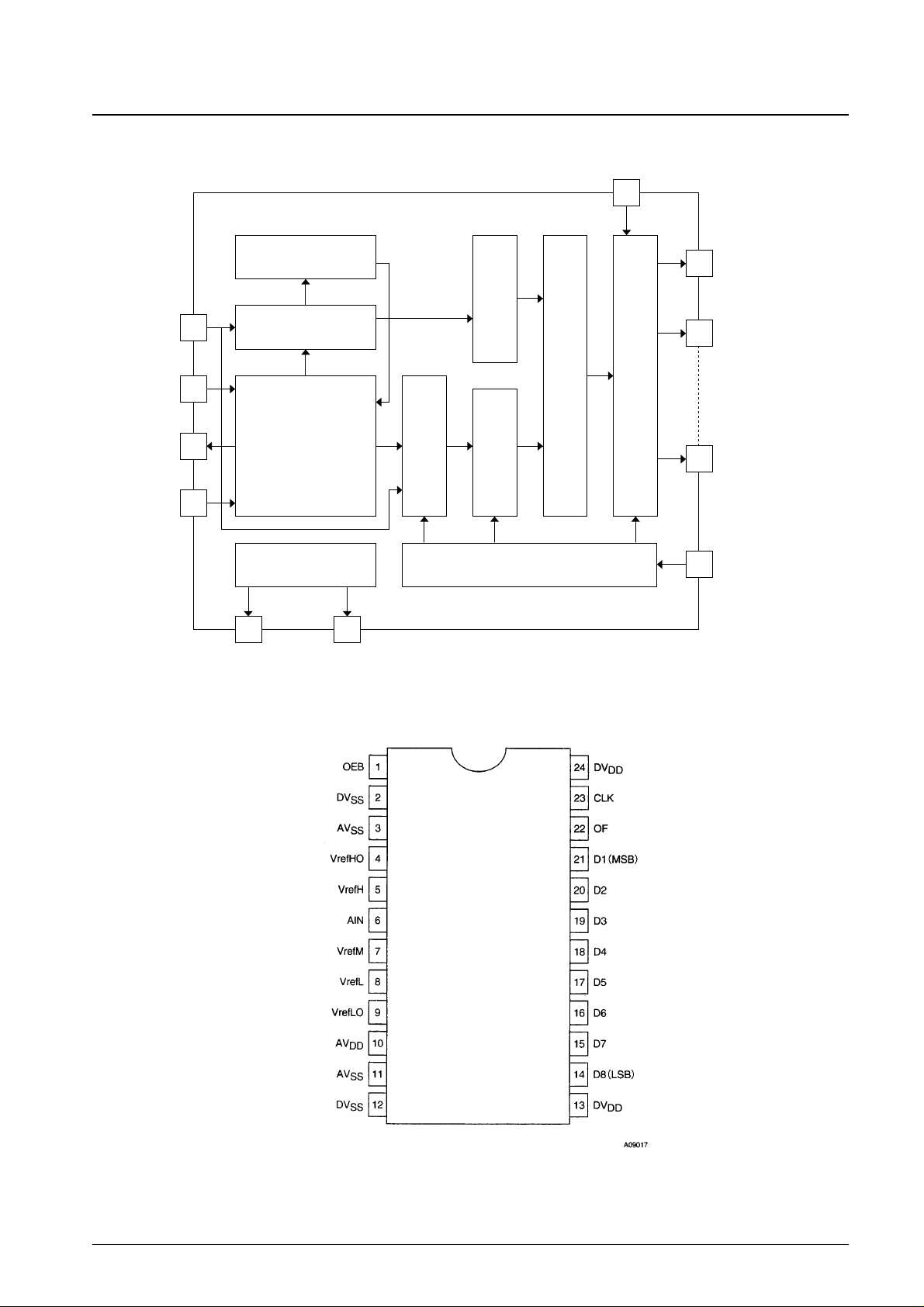
Block Diagram
Lower Vref selection
Upper comparator
Resistor string
Reference voltage
generation
Clock generation
5VrefH
7VrefM
8VrefL
14 D8(LSB)
21 D1(MSB)
22 OF
23 CLK
4
VrefHO
1
OEB
9
VrefLO
6AIN
Lower comparator
Lower encoder
Data correction
Output register
Upper encoder
A09019
Pin Assignment
Top view
Page 5

No. 5428-5/6
LC89086M
Pin Functions
Pin No. Pin name I/O Function
Digital output enable input
1 OEB I High: high-impedance
Low: Normal operation
2 DV
SS
Digital ground
3 AV
SS
Analog ground
4 Vref HO O
Internal reference voltage (high) generation. Shorting this pin to VrefH (pin 5) generates a voltage of 2.0 V.
This pin must be left open when the internally generated potential is not used.
5 Vref H I Reference voltage input (high)
6 AIN I Analog input
7 Vref M O Reference voltage intermediate level tap.
8 Vref L I Reference voltage input (low)
9 Vref LO O
Internal reference voltage (low) generation. Shorting this pin to VrefL (pin 8) generates a voltage of 0 V.
This pin must be left open when the internally generated potential is not used.
10 AV
DD
Analog power supply
11 AV
SS
Analog ground
12 DV
SS
Digital ground
13 DV
DD
Digital power supply
14 D8 O Digital output (LSB)
15 D7 O Digital output
16 D6 O Digital output
17 D5 O Digital output
18 D4 O Digital output
19 D3 O Digital output
20 D2 O Digital output
21 D1 O Digital output (MSB)
22 OF O Digital output (Overflow)
23 CLK I Clock input
24 DV
DD
Digital power supply
Note: There must be no potential difference between the digital system and analog system VDDand VSSpower supply potentials.
I/O Code Table
The table below lists the relationship between the input and output when VrefH and VrefL are set up so that the zero
transient voltage is 0.000 V and the full-scale transient voltage is 2.008V.
Analog input Digital output
V
AIN
(V) OF D1 D2 D3 D4 D5 D6 D7 D8
Up to 0.000 0 0 0 0 0 0 0 0 0
Up to 0.008 0 0 0 0 0 0 0 0 0
Up to 0.016 0 0 0 0 0 0 0 0 1
Up to 0.024 0 0 0 0 0 0 0 1 0
Up to 0.032 0 0 0 0 0 0 0 1 1
to
Up to 0.992 0 0 1 1 1 1 1 1 0
Up to 1.000 0 0 1 1 1 1 1 1 1
Up to 1.008 0 1 0 0 0 0 0 0 0
Up to 1.016 0 1 0 0 0 0 0 0 1
to
Up to 1.992 0 1 1 1 1 1 1 0 1
Up to 2.000 0 1 1 1 1 1 1 1 0
Up to 2.008 0 1 1 1 1 1 1 1 1
Over 2.008 1 1 1 1 1 1 1 1 1
Page 6

No. 5428-6/6
LC89086M
This catalog provides information as of October, 1997. Specifications and information herein are subject to
change without notice.
■ No products described or contained herein are intended for use in surgical implants, life-support systems, aerospace
equipment, nuclear power control systems, vehicles, disaster/crime-prevention equipment and the like, the failure of
which may directly or indirectly cause injury, death or property loss.
■ Anyone purchasing any products described or contained herein for an above-mentioned use shall:
➀ Accept full responsibility and indemnify and defend SANYO ELECTRIC CO., LTD., its affiliates, subsidiaries and
distributors and all their officers and employees, jointly and severally, against any and all claims and litigation and all
damages, cost and expenses associated with such use:
➁ Not impose any responsibility for any fault or negligence which may be cited in any such claim or litigation on
SANYO ELECTRIC CO., LTD., its affiliates, subsidiaries and distributors or any of their officers and employees
jointly or severally.
■ Information (including circuit diagrams and circuit parameters) herein is for example only; it is not guaranteed for
volume production. SANYO believes information herein is accurate and reliable, but no guarantees are made or implied
regarding its use or any infringements of intellectual property rights or other rights of third parties.
Sample Application Circuit
Note 1. The value of the reference resistor is about 300 Ω. When this circuit is used with (VrefH – VrefL) = 2 V, a current of 6.7 mA will flow. Use an
operational amplifier or emitter follower with at least this current capacity.
2. The analog input impedance is lower for AC inputs. Therefore, an operational amplifier or emitter follower with a high slew rate and a wide
bandwidth must be used in the previous stage output, and the impedance must be reduced to under 100 Ω.
: Digital V
(5V)
DD
Analog in
*1
*2
*1
Output enable in
100 µ 0.01 µ
10 µ
CLAMP
100 µ 0.01 µ
1 µ
100 µ 0.01 µ
OEB
1
2
SS
AV
3
SS
VrefHO
4
VrefH
5
AIN
6
VrefM
7
VrefL
8
VrefLO
9
AV
10 15
DD
AV
11 14
SS
12 13
DV
SS
100 µ
DV
24
DD
CLKDV
23
OF
22
D1
21
(MSB)
D2
20
D3
19
D4
18
D5
17
D6
LC89086M
16
D7
D8
(LSB)
DV
DD
0.01 µ
Clock in
Overflow flag out
Digital out
Unit (capacitance: F)
: Analog V
(5V)
DD
: Digital Ground
: Analog Ground
 Loading...