

Page 1
CMOS LSI
Ordering number : EN*5543
N3097HA (OT) No. 5543-1/15
Preliminary
SANYO Electric Co.,Ltd. Semiconductor Bussiness Headquarters
TOKYO OFFICE Tokyo Bldg., 1-10, 1 Chome, Ueno, Taito-ku, TOKYO, 110 JAPAN
Digital Audio Interface Receiver
LC89051V
Overview
The LC89051V is for use in IEC958 format data
transmission between digital audio equipment. This LSI is
used on the receiving side, and handles synchronization
with the input signal and demodulation of that signal to a
normal format signal.
Features
• On-chip PLL circuit synchronizes with the transmitted
IEC958 format signal.
• Low-voltage operation (3.3 V)
• Provides 128fs, bit, and L/R clock outputs.
• System clock can be selected to be either 384fs or 512fs.
• Microcontroller interface code settings for different
output types
— Input pin, emphasis output, input bi-phase data
output, and validity flag output settings
— Audio data output format setting
— Channel status output (32-bit output for consumer
products)
— Subcode Q output with CRC flags (80 bits)
— Start ID and shortening (skip) ID detection for DAT
with subcodes
• The built-in VCO can receive at speeds up to twice fs
only when operating from a 5-V power supply.
• Miniature package: SSOP-24
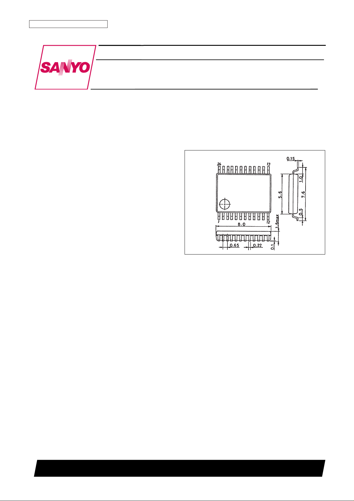
Package Dimensions
unit: mm
3175A-SSOP24
SANYO: SSOP24
[LC89051V]
Page 2
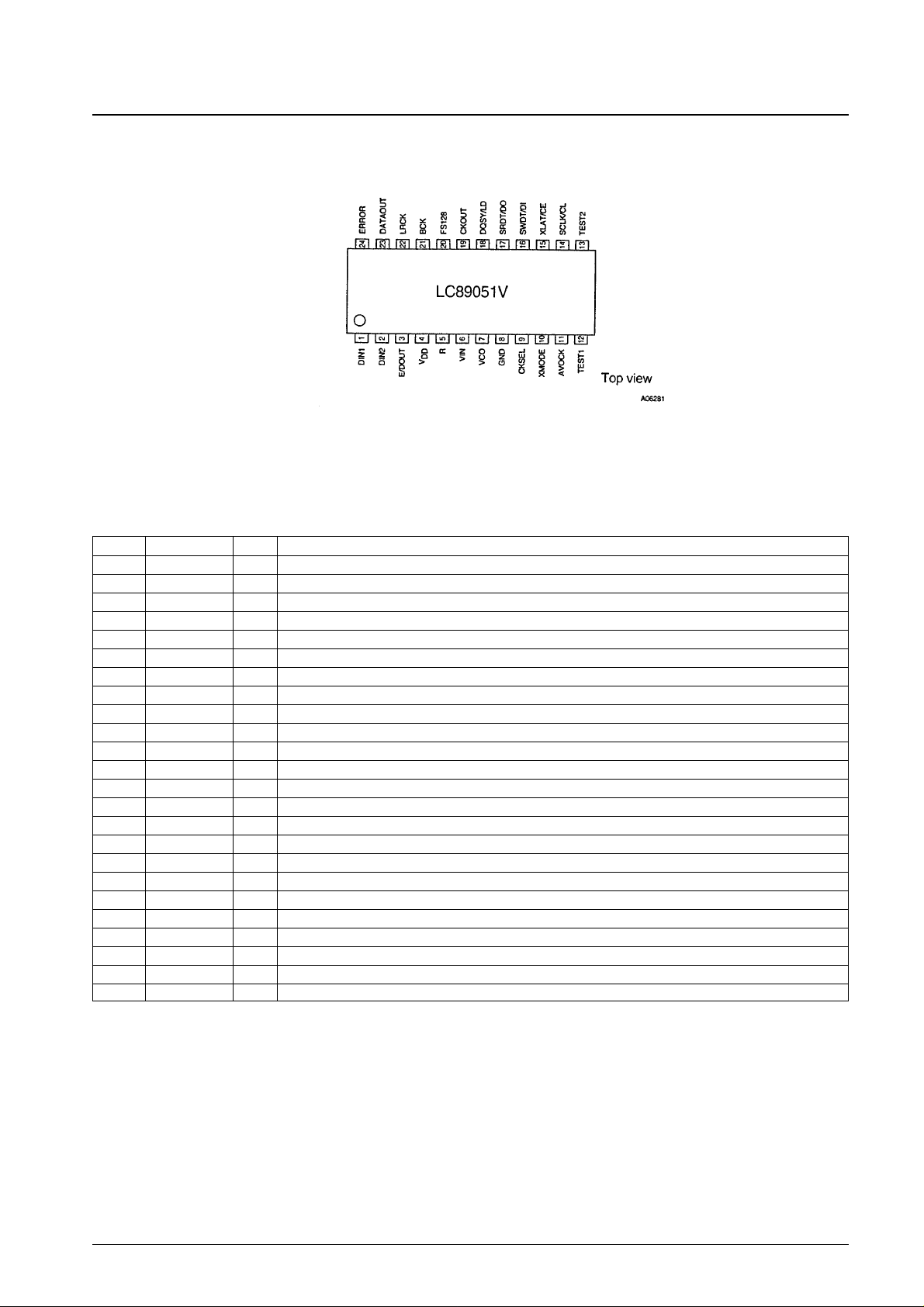
Pin Assignment
Pin Functions
No. 5543-2/15
LC89051V
Pin No. Symbol I/O Description
1 DIN1 I Data input with built-in amplifier (for coaxial or optical module input)
2 DIN2 I Data input (for optical module input)
3 E/DOUT O Emphasis, input bi-phase, and validity flag output
4 V
DD
– Power supply
5 R I VCO gain control input
6 VIN I VCO free-running setting input
7 VCO O PLL low-pass filter setting
8 GND – Ground
9 CKSEL I System clock selection input (384fs or 512fs)
10 XMODE I Reset input
11 AVOCK I PLL error lock avoidance clock input
12 TEST1 I Test input (Must be connected to ground in normal operation)
13 TEST2 I Test input (Must be connected to ground in normal operation)
14 SCLK/CL I Microcontroller interface clock input
15 XLAT/CE I Microcontroller interface latch/chip enable input
16 SWDT/DI I Microcontroller interface write data input
17 SRDT/DO O Microcontroller interface read data output
18 DQSY/LD O Microcontroller interface subcode Q and ID synchronization output
19 CKOUT O VCO clock output (free running, 384fs, or 512fs)
20 FS128 O 128fs clock output
21 BCK O Bit clock output
22 LRCK O L/R clock output (left channel = high, right channel = low)
23 DATAOUT O Audio data output
24 ERROR O PLL lock error mute output
Page 3
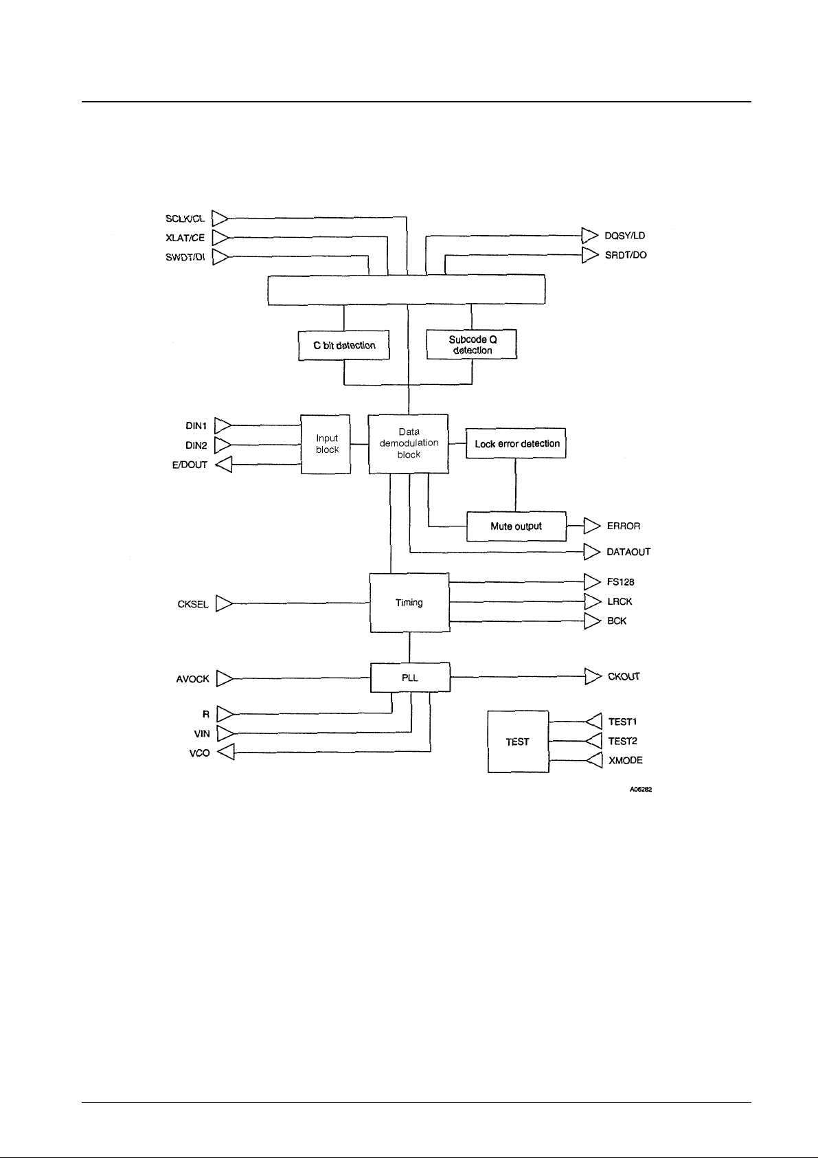
Block Diagram
No. 5543-3/15
LC89051V
Microcontroller interface
Page 4
Specifications
Absolute Maximum Ratings
Allowable Operating Ranges
Electrical Characteristics
DC Characteristics (1) at Ta = –30 to +75°C, VDD= 4.5 to 5.5 V, VSS= 0 V
Note: 1. Applies to the CKSEL, AVOCK, TEST1, and TEST2 pins. CMOS levels.
2. Applies to the XMODE, SCLK/CL, XLAT/CE, SWDT/DI pins. CMOS Schmitt inputs.
3. Applies to the DIN2 pin. TTL Schmitt levels.
4. VDD= 5.0 V, Ta = 25°C, input data fs = 96 kHz
5. Measured before the DIN1 pin input capacitor.
DC Characteristics (2) at Ta = –30 to +75°C, VDD= 3.0 to 3.6 V, VSS= 0 V
Note: 6. Applies to the CKSEL, AVOCK, TEST1, and TEST2 pins. CMOS levels.
7. Applies to the XMODE, SCLK/CL, XLAT/CE, SWDT/DI pins. CMOS Schmitt inputs.
8. Applies to the DIN2 pin. TTL Schmitt levels.
9. VDD= 3.3 V, Ta = 25°C, input data fs = 48 kHz
10. Measured before the DIN1 pin input capacitor.
No. 5543-4/15
LC89051V
Parameter Symbol Conditions Ratings Unit
Supply voltage V
DD
–0.3 to +7.0 V
I/O voltages V
I
, V
O
–0.3 to VDD+ 0.3 V
I/O current I
I
, I
O
±20 mA
Operating temperature Topr –30 to +75 °C
Storage temperature Tstg –55 to +125 °C
Parameter Symbol Conditions min typ max Unit
Supply voltage V
DD
3.0 5.0 5.5 V
(3.3)
Operating temperature T
OPR
–30 +75 C°
Parameter Symbol Conditions min typ max Unit
Input high-level voltage V
IH
1 *1 0.7 V
DD
VDD+ 0.3 V
Input low-level voltage V
IL
1 *1 –0.3 0.3 V
DD
V
Input high-level voltage V
IH
2 *2 0.8 V
DD
VDD+ 0.3 V
Input low-level voltage V
IL
2 *2 –0.3 0.2 V
DD
V
Input high-level voltage V
IH
3 *3 2.5 VDD+ 0.3 V
Input low-level voltage V
IL
3 *3 –0.3 +0.6 V
Output high-level voltage V
OHIOH
= –4 mA V
DD
– 2.1 V
Output low-level voltage V
OL
IOL= 4 mA 0.4 V
Current drain I
DD
*4 20 mA
Input amplitude Vpp *5 0.4 V
DD
+ 0.3 V
Parameter Symbol Conditions min typ max Unit
Input high-level voltage V
IH
1 *6 0.7 V
DD
VDD+ 0.3 V
Input low-level voltage V
IL
1 *6 –0.3 0.2 V
DD
V
Input high-level voltage V
IH
2 *7 0.75 V
DD
VDD+ 0.3 V
Input low-level voltage V
IL
2 *7 –0.3 0.15 V
DD
V
Input high-level voltage V
IH
3 *8 2.4 VDD+ 0.3 V
Input low-level voltage V
IL
3 *8 –0.3 +0.3 V
Output high-level voltage V
OHIOH
= –2 mA V
DD
– 0.8 V
Output low-level voltage V
OL
IOL= 2 mA 0.4 V
Current drain I
DD
*9 10 mA
Input amplitude Vpp *10 0.4 V
DD
+ 0.3 V
Page 5
AC Characteristics (Normal Mode) at Ta = –30 to +75°C, VDD= 3.0 to 5.5 V
Note: 11.Ta = 25°C, VDD= 3.3 V, with the circuit constants for standard speed operation in the sample application circuit.
12.Ta = 25°C, V
DD
= 5.0 V, with the circuit constants for standard speed operation in the sample application circuit.
AC Characteristics (Double Speed Mode) at Ta = –30 to +75°C, VDD= 4.5 to 5.5 V
Note: 13.Ta = 25°C, VDD= 5.0 V, with the circuit constants for 2× speed operation in the sample application circuit.
No. 5543-5/15
LC89051V
Parameter Symbol Conditions min typ max Unit
AVOCK input pulse width t
WBI
10 µs
VCO free-running frequency f
VCO
*11 50 MHz
*12 75 MHz
BCK output pulse width t
WBO
fs = 48 kHz 160 ns
Output data setup time t
DSO
80 ns
Output data hold time t
DHO
80 ns
Output delay t
BD
–10 0 +10 ns
Parameter Symbol Conditions min typ max Unit
AVOCK input pulse width t
WBI
10 µs
VCO free-running frequency f
VCO
*13 80 MHz
BCK output pulse width t
WBO
fs = 96 kHz 80 ns
Output data setup time t
DSO
40 ns
Output data hold time t
DHO
40 ns
Output delay t
BD
–10 0 +10 ns
Page 6

Microcontroller Interface Block AC Characteristics
at Ta = –30 to +75°C, VDD= 3.0 to 5.5 V (when CKSEL is low)
Input mode
Output mode
No. 5543-6/15
LC89051V
Parameter Symbol Conditions min typ max Unit
CL low pulse width t
WL
100 ns
CL high pulse width t
WH
100 ns
Data setup time t
DS
50 ns
Data hold time t
DH
50 ns
CE delay time t
D3
1.0 µs
CL delay time t
D4
50 ns
CE delay time t
D5
100 ns
LD pulse width t
W
fs = 44.1 kHz 136 µs
fs = 88.2 kHz 68 µs
Data delay time t
D1
CL= 30 pF 100 ns
Data delay time t
D2
CL= 30 pF 100 ns
Page 7

Microcontroller Interface Block AC Characteristics
at Ta = –30 to +75°C, VDD= 3.0 to 5.5 V (when CKSEL is high)
Input mode
Output mode
No. 5543-7/15
LC89051V
Parameter Symbol Conditions min typ max Unit
SCLK low pulse width t
WL
100 ns
SCLK high pulse width t
WH
100 ns
Setup time t
DS
50 ns
Hold time t
DH
50 ns
Delay time t
D
100 µs
DQSY pulse width t
W
fs = 44.1 kHz 136 µs
fs = 88.2 kHz 68 µs
XLAT pulse width t
WLA
100 ns
Data delay time t
D1
CL= 30 pF 100 ns
Data delay time t
D2
CL= 30 pF 100 ns
Page 8

Functions
1. Data Input and Output (DIN1, DIN2, E/DOUT)
The DIN1 pin has a built-in amplifier, and can receive signals with an amplitude of about 400 mVp-p (coaxial input).
The DIN2 pin is only for use in optical modules.
Note that although the data input pins are controlled by the microcontroller, DIN1 can be selected when a
microcontroller is not used. The microcontroller interface pins must be tied low in such applications.
The E/DOUT normally outputs channel status information. However, it can be set to output either the input bi-phase
data or the validity flag by command codes from the microcontroller.
2. PLL (R, VIN, VCO, AVOCK)
This circuit includes a built-in VCO and supports sampling frequencies of 32, 44.1, and 48 kHz.
This LSI can also receive at the 2× sampling frequencies of 64 kHz, 88.2 kHz, and 96 kHz, but only when operating
from a 5-V power-supply voltage. However, the demodulated data and clock output during double speed reception
follow the received sampling frequency, and the transmission format for 2×-speed data must follow the IEC958
standard.
The built-in VCO is controlled by the resistors connected to the R and VIN pins.
The resistor connected to R functions as both the VCO gain control and as temperature compensation. The VIN pin
sets the VCO free-running frequency. Recommended circuit constants are shown in the sample application circuit.
Note that the VCO free-running frequency varies with temperature and with manufacturing variations between
samples. The recommended circuit constants shown in the sample application circuit take these variations into
account so that the PLL circuit lockup characteristics are not adversely affected. These values are not designed to
reduce variations in the free-running frequency. The VCO pin is the PLL loop filter pin. The loop filter is formed by
attaching an external capacitor and a resistor to this pin. See the sample application circuit for these circuit constants.
PLL Loop Filter Structure
The PLL circuit will be reset within a fixed period when PLL lock pull-in fails if a continuously operating clock of
no more than 50 kHz is input to the AVOCK pin. This allows incorrect PLL operation to be avoided.
3. Clock Settings and Output (FS128, BCK, LRCK, DATAOUT, CKSEL, CKOUT)
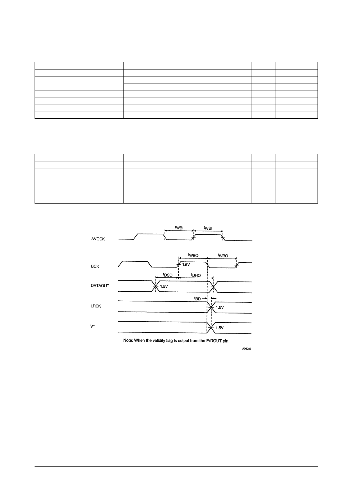
A 128fs clock signal is output from the FS128 pin. Figure 1 shows the output timing for the BCK, LRCK, and
DATAOUT pins.
The CKOUT clock output is set by the CKSEL pin as listed in the table below.
The microcontroller interface format is also set by CKSEL as listed in the table below.
No. 5543-8/15
LC89051V
CKSEL CKOUT
L 384fs clock output
H 512fs clock output
CKSEL Microcontroller interface
L Figure 2
H Figure 3
Page 9

Figure 1 Data Output Timing
No. 5543-9/15
LC89051V
Page 10

Figure 2 Microcontroller Interface Timing 1
No. 5543-10/15
LC89051V
Page 11

Figure 3 Microcontroller Interface Timing 2
No. 5543-11/15
LC89051V
Page 12

Microcontroller Interface (SCLK/CL, XLAT/CE, SWDT/DI, SRDT/DO, DQSY/LD)
1. Data input and output addresses are allocated as follows:
2. The input command codes control the following setting:
• System stop
• Data input pin setting
• Input bi-phase data output selection
• Validity flag output selection
• Audio data output format setting
DI1: Stops VCO operation and thus stops the system.
DI2: Selects which input data to demodulate.
DI3 and DI4: Select the E/DOUT pin output.
DI5 and DI6: Set the audio data output format.
All bits are set low immediately after XMODE is switched from low to high. DI0 and DI7 are not used.
No. 5543-12/15
LC89051V
Data input or output
Figure 2: Microcontroller Interface Timing 1 Figure 3: Microcontroller Interface Timing 2
B0 B1 B2 B3 A0 A1 A2 A3 B0 B1 B2 B3 A0 A1 A2 A3
Data input F7 1 1 1 0 1 1 1 1 EA 0 1 0 1 0 1 1 1
C bit output F8 0 0 0 1 1 1 1 1 E9 1 0 0 1 0 1 1 1
Subcode Q, ID output F9 1 0 0 1 1 1 1 1 E8 0 0 0 1 0 1 1 1
DI1 L H
System Operating Stopped
DI2 L H
Data demodulation input DIN1 DIN2
DI3 L H
DI4 L H L H
E/DOUT
Emphasis Validity DIN1 input DIN2 input
data output flag output data output data output
DI5 L H
DI6 L H L H
16-bit right- 20-bit right- 20-bit right- 20-bit left-
DATAOUT justified justified justified justified
MSB first LSB first MSB first MSB first
Page 13

3. The following output settings can be controlled:
• Channel status (C bit) output
• Subcode Q data output
• Start ID and shortening ID detection for DAT with subcodes
C bit output
• This IC only handles the first 32 bits.
• The flag is fixed at the high level (only when CKSEL is high), and the data format is LSB first.
• Error and update checking is not applied to the data.
• The internal shift register is reset if a PLL lock error occurs.
• Since the channel status information consists of 192 frames, a fixed period must be provided between data readout
operations.
1
fs
× 192 (ms) < (the interval between data readout operations)
Subcode Q output
• Subcode Q can be read out after the fall of the DQSY/LD signal. Also note that the data is updated every time this
signal falls. However, this signal will not be output (fall) unless 96-bit subcode Q data (including the CRC check
bits) is input.
• The flag outputs a high when the CRC check passes, and low if the CRC check fails. Besides, the shift clock SCLK
is required to be input regardless of the CRC flag status after latch pulse input.
• The bit order is LSB first within each byte of the 80 bits of subcode Q data.
ID detection
• The start ID and shortening ID are only detected when the DAT category code (1100000L) is received.
• These IDs are detected as follows:
— A low pulse is output from DQSY/LD if a start ID (R0) or a shortening ID (L1) is detected following a sync
signal (L0).
— After this signal, data can be read out from SRDT/DO by inputting the same address value as that used for
subcode Q data to SWDT/DI.
Figure 4 User Data for DAT with Subcodes
• The table below shows the relationship between the sync signal (L0), the start ID (R0), the shortening ID (L1), and
the data output.
• Output pins
The output scheme used for SRDT/DO differs depending on the microcontroller interface format selected by
No. 5543-13/15
LC89051V
(L0): SYNC H H
(R
0
): Start ID H L
(L
1
): Shortening ID L H
Flags + 80 data bits all H all L
Detected ID Start ID Shortening ID
CKSEL Format SRDT/DO
L Figure 2 High open-drain output
H Figure 3 Three-state output
Page 14

Error (ERROR)
The ERROR pin goes high if there is an error in the input data or if the PLL is unlocked. It holds the high level for about
100 to 300 ms after data demodulation returns to normal and then goes low. The table below lists the data processing
when an error has occurred.
System Reset (XMODE)
Normal system operation is started by setting XMODE high after the power supply has risen above at least 4.5 V
(3.0 V). After power is applied, the system will be reset if a low level is applied once more to the XMODE pin. If
XMODE is set low, the VCO free-running oscillator clock is output from CKOUT.
Figure 5 XMODE Pin Operation
No. 5543-14/15
LC89051V
Type of error DATAOUT C bit Sub Q ID E/DOUT
Up to 8 consecutive parity errors Previous data value Output Output Output Output
Over 8 consecutive parity errors L Output Output Output Output
PLL lock error L L L L L
Page 15

Sample Application Circuit
No. 5543-15/15
LC89051V
Value
Item Symbol 5.0-V operation 3.3-V operation
Standard speed 2× speed Standard speed
R1 24 kΩ 24 kΩ 24 kΩ
Resistors
R2 5.1 kΩ 5.1 kΩ 5.1 kΩ
R3 5.1 kΩ 12 kΩ 5.1 kΩ
R4 150 Ω 150 Ω 150 Ω
Capacitors
C1 0.1µF 0.1µF 0.1µF
C2 0.01 µF 0.01 µF 0.01 µF
Circuit constants
This catalog provides information as of November, 1997. Specifications and information herein are subject to
change without notice.
■ No products described or contained herein are intended for use in surgical implants, life-support systems, aerospace
equipment, nuclear power control systems, vehicles, disaster/crime-prevention equipment and the like, the failure of
which may directly or indirectly cause injury, death or property loss.
■ Anyone purchasing any products described or contained herein for an above-mentioned use shall:
➀ Accept full responsibility and indemnify and defend SANYO ELECTRIC CO., LTD., its affiliates, subsidiaries and
distributors and all their officers and employees, jointly and severally, against any and all claims and litigation and all
damages, cost and expenses associated with such use:
➁ Not impose any responsibility for any fault or negligence which may be cited in any such claim or litigation on
SANYO ELECTRIC CO., LTD., its affiliates, subsidiaries and distributors or any of their officers and employees
jointly or severally.
■ Information (including circuit diagrams and circuit parameters) herein is for example only; it is not guaranteed for
volume production. SANYO believes information herein is accurate and reliable, but no guarantees are made or implied
regarding its use or any infringements of intellectual property rights or other rights of third parties.
 Loading...