

Page 1

Ordering number : EN*5014B
73096HA (OT) No. 5014-1/20
Overview
The LC8904Q demodulates data transmitted between
digital audio equipment in the EIAJ format (CP-1201) to a
normal format signal synchronized with the receiving side
input signal.
Features
• Synchronizes with the transmitted EIAJ format signal
using a built-in PLL circuit.
• Modes are set up and codes are output according to
commands sent over a microprocessor interface.
— Input pin and output data format setup
— Selection of digital source mode or analog source
mode
— 32-bit channel status output (consumer product
mode 0)
— 80-bit subcode Q data output (CRC check included)
• Either a 384fs or a 512fs clock can be selected as the
system clock.
• Provides 256fs, 128fs, BCLK, and LRCK clock outputs.
• Implements a CD subcode interface (CP-2401) using
user bits.
• Fabricated in a CMOS single-voltage power supply
process
• Package: QFP-48E
Package Dimensions
unit: mm
3156-QFP48E
Preliminary
SANYO: QIP48E
[LC8904Q]
LC8904Q
SANYO Electric Co.,Ltd. Semiconductor Bussiness Headquarters
TOKYO OFFICE Tokyo Bldg., 1-10, 1 Chome, Ueno, Taito-ku, TOKYO, 110-0005 JAPAN
Digital Audio Interface Receiver
CMOS LSI
• CCB is a trademark of SANYO ELECTRIC CO., LTD.
• CCB is SANYO’s original bus format and all the bus
addresses are controlled by SANYO.
Page 2
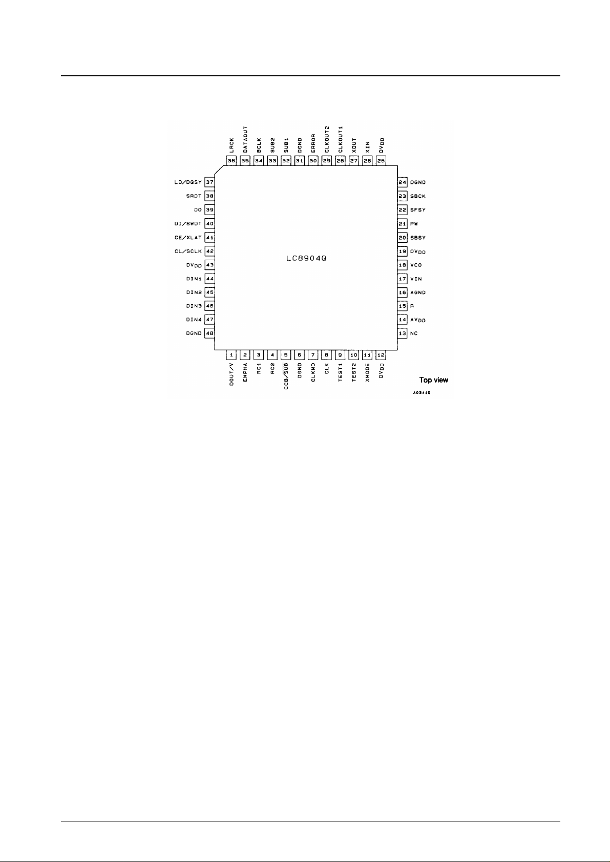
Pin Assignment
No. 5014-2/20
LC8904Q
Page 3
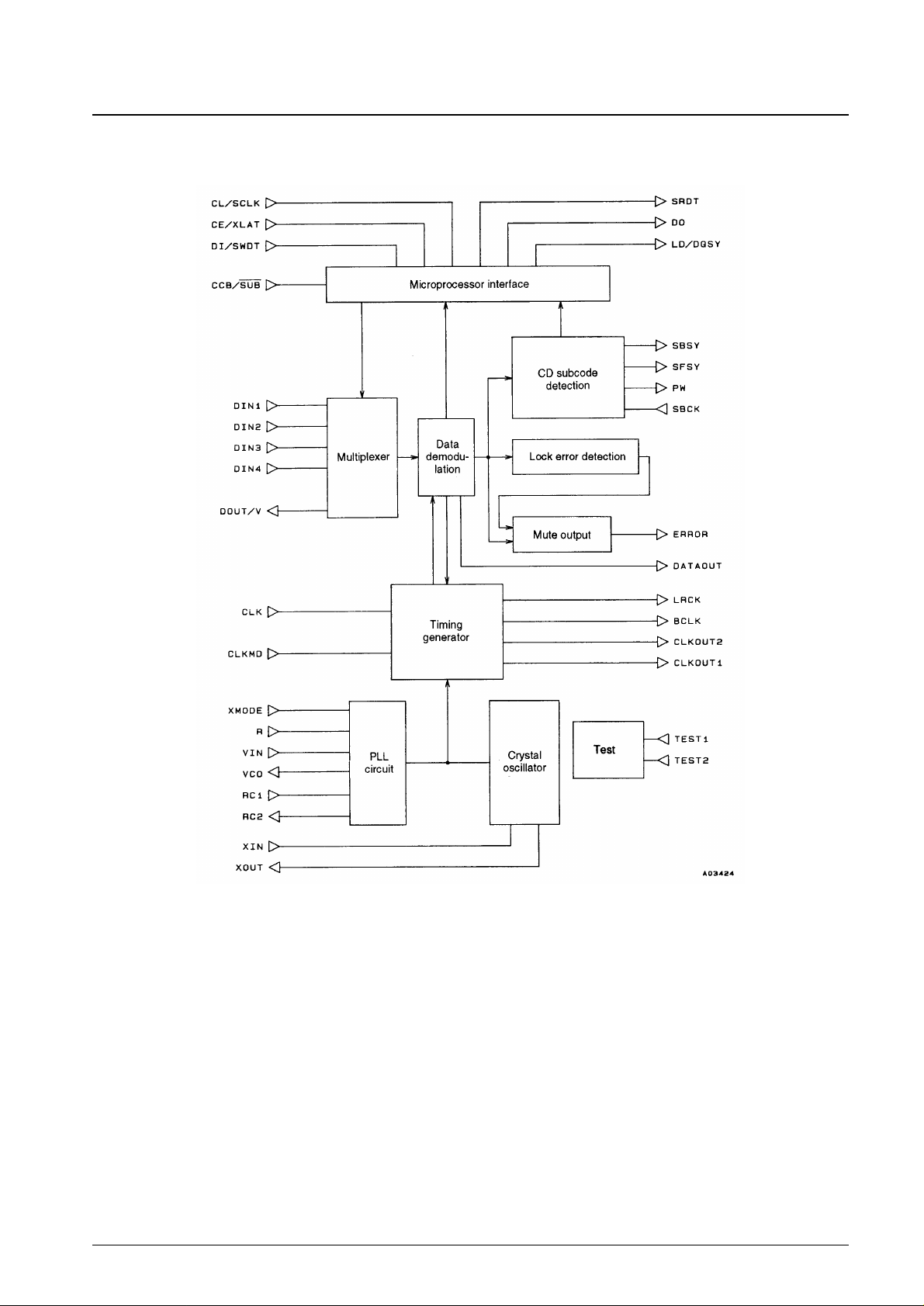
Block Diagram
No. 5014-3/20
LC8904Q
Page 4

Pin Functions
No. 5014-4/20
LC8904Q
No. Symbol I/O Function
1 DOUT/V O EIAJ data and validity flag output
2 EMPHA O Emphasis monitor output (High: emphasis applied)
3 RC1 I CR oscillator input
4 RC2 O CR oscillator output
5 CCB/SUB I Microprocessor interface selection input (High: CCB, low: SUB)
6 DGND Digital system ground
7 CLKMD I Clock output switching (High: 256fs, low: 128fs)
8 CLK I Clock switching input (High: 512fs, low: 384fs)
9 TEST1 I Test pin (Must be tied low during normal operation.)
10 TEST2 I Test pin (Must be tied low during normal operation.)
11 XMODE I Reset input
12 DV
DD
Digital system power supply
13 NC No connection
14 AV
DD
Analog system power supply
15 R I VCO oscillator band adjustment input
16 AGND Analog system ground
17 VIN I VCO free-running frequency setting input
18 VCO O PLL low-pass filter connection
19 DV
DD
Digital system power supply
20 SBSY O CD subcode interface: block sync output
21 PW O CD subcode interface: data output
22 SFSY O CD subcode interface: frame sync output
23 SBCK I CD subcode interface: data read shift clock input
24 DGND Digital system ground
25 DV
DD
Digital system power supply
26 XIN I Crystal oscillator input
27 XOUT O Crystal oscillator output
28 CLKOUT1 O VCO and crystal oscillator clock output
29 CLKOUT2 O 256fs or 128fs clock output (selected by CLKMD)
30 ERROR O Error mute output
31 DGND Digital system ground
32 SUB1 O Sampling frequency monitor output
33 SUB2 O Sampling frequency monitor output
34 BCLK O Bit clock output
35 DATAOUT O Audio data output
36 LRCK O L/R clock output (High: left channel, low: right channel)
37 LD/DQSY O Microprocessor interface: subcode Q data sync output
38 SRDT O Microprocessor interface: data output when CCB/SUB is low (3-state output)
39 DO O Microprocessor interface: data output when CCB/SUB is high (High-level open drain output)
40 DI/SWDT I Microprocessor interface: data input
41 CE/XLAT I Microprocessor interface: chip enable/latch input
42 CL/SCLK I Microprocessor interface: clock input
43 DV
DD
Digital system power supply
44 DIN1 I Data input with built-in amplifier
45 DIN2 I Data input with built-in amplifier
46 DIN3 I Data input with built-in amplifier
47 DIN4 I Data input with built-in amplifier
48 DGND Digital system ground
Page 5
Specifications
Absolute Maximum Ratings at Ta = 25°C
Allowable Operating Ranges
Electrical Characteristics
DC Characteristics at Ta = –30 to +75°C, VDD= 4.5 to 5.5 V
Note: 1. Input pins other than DIN1, DIN2, DIN3, DIN4, RC1, and XMODE. TTL compatible.
2. The XIN pin. CMOS compatible.
3. The XMODE and RC1 pins. CMOS Schmitt compatible.
4. V
DD
= 5.0 V, Ta = 25°C, and input data with an fs of 48 kHz.
5. Conditions prior to the capacitances of the DIN1, DIN2, DIN3, and DIN4 pins.
No. 5014-5/20
LC8904Q
Parameter Symbol Conditions Ratings Unit
Maximum supply voltage V
DD
max –0.3 to +7.0 V
Input and output voltage V
I
· V
O
–0.3 to VDD+ 0.3 V
Operating temperature Topr –30 to +75 °C
Storage temperature Tstg –55 to +125 °C
Parameter Symbol Conditions min typ max Unit
Supply voltage V
DD
4.5 5.0 5.5 V
Parameter Symbol Conditions min typ max Unit
Input high-level voltage V
IH
1 *1 2.2 VDD+ 0.3 V
Input low-level voltage V
IL
1 *1 –0.3 +0.8 V
Input high-level voltage V
IH
2 *2 0.7 V
DD
VDD+ 0.3 V
Input low-level voltage V
IL
2 *2 –0.3 0.3 V
DD
V
Input high-level voltage V
IH
3 *3 0.8 V
DD
VDD+ 0.3 V
Input low-level voltage V
IL
3 *3 –0.3 0.2 V
DD
V
Output high-level voltage V
OHIOH
= –1 µA VDD– 0.05 V
Output low-level voltage V
OL
IOL= 1 µA VSS+ 0.05 V
Current drain I
DD
*4 30 45 mA
Input amplitude V
PP
*5 0.4 VDD+ 0.3 V
Page 6

AC Characteristics at Ta = –30 to +75°C, VDD= 4.5 to 5.5 V
Note: When the validity fag is output from the DOUT/V pin.
No. 5014-6/20
LC8904Q
Parameter Symbol Conditions min typ max Unit
Output pulse width t
WBO
fs = 48 kHz, load = 30 pF 160 ns
Output data setup time t
DSO
fs = 48 kHz, load = 30 pF 80 ns
Output data hold time t
DHO
fs = 48 kHz, load = 30 pF 80 ns
Page 7

Microprocessor Interface AC Characteristics (when CCB/SUB is low)
at Ta = –30 to +75°C, VDD= 4.5 to 5.5 V
No. 5014-7/20
LC8904Q
Parameter Symbol Conditions min typ max Unit
SCLK low-level pulse width t
WL
100 ns
SCLK high-level pulse width t
WH
100 ns
Setup time t
DS
50 ns
Hold time t
DH
50 ns
Delay time t
D
100 ns
Latch pulse time t
WLA
100 ns
DQSY pulse time t
W
fs = 44.1 kHz 136 µs
Data delay time t
D1
CL= 30 pF 75 ns
Data delay time t
D2
CL= 30 pF 75 ns
Page 8

Microprocessor Interface AC Characteristics (when CCB/SUB is high)
at Ta = –30 to +75°C, VDD= 4.5 to 5.5 V
Note 1. C bit output
2. Subcode Q output
No. 5014-8/20
LC8904Q
Parameter Symbol Conditions min typ max Unit
CL low-level pulse width t
WL
100 ns
CL high-level pulse width t
WH
100 ns
Data setup time t
DS
50 ns
Data hold time t
DH
50 ns
CE delay time t
D3
1.0 µs
CL delay time t
D4
50 ns
CE delay time t
D5
100 ns
LD pulse time t
W
fs = 44.1 kHz 136 µs
Data delay time t
D1
CL= 30 pF 75 ns
Data delay time t
D2
CL= 30 pF 75 ns
Page 9

CD Subcode Interface AC Characteristics at Ta = –30 to +75°C, VDD= 4.5 to 5.5 V
No. 5014-9/20
LC8904Q
Parameter Symbol Conditions min typ max Unit
SBSY block period t
B
12.0 13.3 14.7 ms
SBSY pulse width t
BW
*1 110 µs
SFSY frame period t
F
*2 90 136 165 µs
SFSY high-level pulse width t
FHW
4 µs
SFSY low-level pulse width t
FLW
1.5 µs
SBCK high-level pulse width t
CHW
*3 2.0 4.0 5.0 µs
SBCK low-level pulse width t
CLW
*3 2.0 4.0 5.0 µs
SBCK rise time t
rC
30 ns
SBCK fall time t
fC
30 ns
SBCK delay time t
CD
*3 10 20 30 µs
P data access time t
PAC
3 10 µs
Data hold time t
HD
0 µs
Page 10

The LC8904Q subcode interface uses the user bit subcode sync word and start bit for system timing extraction.
Therefore, since SBSY and SFSY will change with that timing, user bit transmission must follow the table shown below
when using the values of tBW, tF, t
CHW
, t
CLW
, and tCDwith the specifications listed in the preceding tables.
Note: 1. The subcode sync word is defined as the block sync section (block start) when 0-valued data has been received consecutively for at least 22 bits.
2. The period of the frame sync signal S0 is 90.7 µs. The S1 period also has a minimum length of 90.7 µs (when 0-valued data is received
consecutively for 22 bits), depending on the subcode sync word period. Not that the shortest word is 10 bits.
3. The SBCK signal input delay (t
HD
) and pulse widths (t
CHW
and t
CLW
) must be set to values less than or equal to the typical values when the
shortest user data word length is used.
No. 5014-10/20
LC8904Q
Page 11

No. 5014-11/20
LC8904Q
Microprocessor Interface
1. When CCB/SUB is low
Page 12

No. 5014-12/20
LC8904Q
2. When CCB/SUB is high
Page 13

The microprocessor interface controls the following settings and outputs.
1. System stop
2. Data input pin settings
3. Validity flag (V flag) output selection
4. Analog source mode setting
5. Output data format setting
6. Channel status (32 bits) output
7. Output of the 80-bit subcode Q data with CRC flags.
• CCB/SUB pin
The CCB/SUB pin selects one of two formats. The clocks and codes must be set up appropriately for each of these
formats. SRDT is the output pin when CCB/SUB is low. SRDT goes to the high-impedance state when the
CCB/SUB pin is high, during writes, and when an address for a different output is latched. In contrast with the
SRT pin, the DO pin is a high-level open drain output that functions as the output pin when CCB/SUB is high.
• Data I/O address
Address are allocated according to the differing formats as listed below.
• Input
The DIN1 to DIN4 data input pins have built-in amplifiers, and can accept signals with amplitudes of about
400 Vp-p. Note that the DOUT pin can be set up to output the EIAJ format data by microprocessor interface
commands. (It can also be used to output the V flag.)
• Input code settings
System stop by stopping both the VCO and crystal oscillators (DI4)
Selection of data to demodulate (DI5, DI6)
Input data (EIAJ format) output selection
No. 5014-13/20
LC8904Q
Format CCB/SUB = low CCB/SUB = high
I/O B0 B1 B2 B3 A0 A1 A2 A3 B0 B1 B2 B3 A0 A1 A2 A3
Data input EA 0 1 0 1 0 1 1 1 F7 1 1 1 0 1 1 1 1
Data output (C bits) E9 1 0 0 1 0 1 1 1 F8 0 0 0 1 1 1 1 1
Data output (subcode Q) E8 0 0 0 1 0 1 1 1 F9 1 0 0 1 1 1 1 1
DI4 L H
System Run Stop
DI5 L H L H
DI6 L L H H
Demodulation data input DIN1 DIN2 DIN3 DIN4
DI7 L H L H
DI8 L L H H
DOUT/V pin DIN1 DIN2 DIN3 DIN4
Page 14

V flag output selection (DI9)
Source selection (DI10)
Audio data output format setting (DI11, DI12, DI13)
DI4 to DI13 are set to an initial value of low, immediately after the XMODE pin goes from low to high. Since DI0
to DI3 and DI14 to DI15 are unused they can be set to either low or high.
• Output
C bits
— This product only supports 32 bits, since it is designed for mode 0 consumer applications.
— In readout when CCB/SUB is low, after the output address is loaded into SWDT, the flag (fixed at the high
level) is output on the fall of XLAT, and then 32 bits of data is output according to SCLK.
— In readout when CCB/SUB is high, after the output address is loaded into DI, the 32 bits of data are output
from DO according to CL while CE is high.
— Since the C bits are not checked for errors, processing is performed after the PLL lock state is detected.
Therefore, data must be read out only after the ERROR pin goes low.
— If a lock error occurs during readout (ERROR = high), the shift register will be reset and all data will become 0
(low). However, while the ERROR pin will also go high on a parity error, this error processing will not be
performed.
— An interval of at least 6 ms or longer must be provided between readout operations.
Subcode Q
— The LC8904Q provides the following two functions for subcode readout:
1. CD subcode interface (CP-2401) is possible
2. Output of subcode Q data with CRC flags included, which corresponds to the CD and MD formats
The microprocessor interface uses the readout function of item 2.
— The subcode Q data, which is reproduced at 1 bit per frame, is input to an 80-bit register and a CRC checking
circuit. After the 96 bits of data have been input, it is loaded into a shift register on the falling edge of
LD/DQSY. The data must be read out after this load operation.
— In readout when CCB/SUB is low, after the output address has been loaded into SWDT, the CRC flags are
output on the falling edge of XLAT. If the CRC flags indicate that the check was OK, a high level is output.
Next, 80 bits of data is output from SRDT according to SCLK. Note that the subcode Q data is updated on
every falling edge of the DQSY signal.
— Readout when CCB/SUB is high is identical to that described in item 3. (See the timing charts for details.)
— The data output from SRDT (DO) has the same order on a per-byte basis, but the bit order within each byte is
LSB first.
— If a lock error occurs between the fall of DQSY and the fall of XLAT, the CRC flags will go low. However, if
a lock error after the fall of XLAT, the CRC flags will not go low, since correct data will be output.
No. 5014-14/20
LC8904Q
DI9 L H
DOUT/V pin Data selected by DI7 and DI8 V flag
DI10 L H
Mode Digital source Analog source
DI11 L L H H H H
DI12 L L L H L H
DI13 L H L L H H
16 bits 16 bits 20 bits 20 bits 20 bits 20 bits
DATAOUT MSB first MSB first MSB first LSB first MSB first LSB first
Rear packed Front packed Rear packed Rear packed Front packed Front packed
Page 15

— When the 96 bits of the subcode Q data have been read in with the PLL circuit in the locked state, a sync signal
that has a low period with a pulse width of 136 µs is output by outputting at least 22 bits of continuous 0-valued
data after the 96 bits of W data (W97) from DQSY. Note that this sync signal low-level pulse will not be output
unless 96 bits of subcode Q data including the CRC flags are input.
When not Using the Microprocessor Interface
If the LC8904Q is used without using the microprocessor interface, the microprocessor interface pins must be tied to
fixed levels and data only input to pin DIN1. This configuration can be useful as a simplified circuit evaluation method.
CD Subcode Interface
The LC8904Q outputs CD subcode data from the SFSY, SBCK, PW, and SBSY pins. These pins output user bits that
were transmitted according to the CP-1201 standard and that were converted to the CP-2401 standard.
The timing of the rise and fall of the SFSY signal is converted into that shown in the figure below according to the
timing of the start bit in the user bits in the input data.
No. 5014-15/20
LC8904Q
Page 16

The CLK, CLKMD, CLKOUT1, and CLKOUT2 Pins
The output clocks for the CLKOUT1 and CLKOUT2 clock output pins is selected by the CLK and CLKMD pins.
Note: 1. The crystal oscillator clock is output in analog source mode.
2. The 256fs clock has a H:L duty ratio of 2:1 when the CLK pin is low.
The SUB1 and SUB2 Pins
These pins indicate the sampling frequency of the input data.
The state “#1” is indicated on a PLL lock error and in analog source mode.
Also note that the DATAOUT and EMPHA pins will output low levels in this state.
The EMPHA Pin
The ERROR pin and Error Processing
ERROR pin: When an error exists in the input data or when the PLL circuit is in the unlocked state, this pin goes high
and holds that high level for about 200 to 300 ms after data demodulation returns to normal. The table below lists the
data processing applied when an error occurs.
Note: * The CRC flags go low when a PLL lock error occurs.
Note: PLL lock error determination is performed starting from preamble detection.
The XMODE Pin
This pin is used for system reset. The system will start to operate normally if this pin is set high after the power supply
has risen to at least 4.5 V. If XMODE is set low, the VCO free-running clock will be output from the CLKOUT1 pin.
After application of power, the system will be reset if the XMODE pin is set low again.
No. 5014-16/20
LC8904Q
CLK CLKOUT
*1
L Outputs a 384fs clock
H Outputs a 512fs clock
CLKMD CLKOUT2
L Outputs a 256fs clock
*2
H Outputs a 128fs clock
Pin 32 kHz 44.1 kHz 48 kHz #1
SUB1 H L L H
SUB2 H L H L
Pin Emphasis applied Emphasis not applied Analog source mode
EMPHA H L L
Type of error DATAOUT SUB1, SUB2 C bit Sub Q*
Up to eight consecutive parity errors Previous data Output Output Output
Eight or more consecutive parity errors L Output Output Output
PLL lock error L #1 L L
Page 17

Analog Source Mode
The LC8904Q enters analog source mode in the following two cases:
1. Analog source mode is selected from the microprocessor interface.
2. If the input pin specified for data demodulation goes to the no signal state.
In this mode, the clock that operates the whole system is taken from the crystal oscillator clock, and the PLL and data
demodulation circuits are stopped. The BCLK, LRCK, CLKOUT1, and CLKOUT2 clocks are output.
The output pins have the following functions in analog source mode:
1. DOUT/V
Data output as specified by the microprocessor interface
2. ERROR
Outputs the error state, i.e. a high level.
3. SUB1 and SUB2
These pins output the “#1” lock error state.
4. DATAOUT
Outputs the lock error state, i.e., a low level.
5. EMPHA
Outputs the lock error state, i.e., a low level.
6. Microprocessor interface codes
Input codes: The codes loaded from the microprocessor interface are retained.
Output codes: The same codes as output for a PLL lock error.
Crystal Oscillator
1. A built-in detector circuit determines whether or not a data input signal is present. This circuit operates from either
the VCO or the crystal oscillator clock. When the power supply is coming up, this clock is supplied from the VCO,
and if a no-data state is detected, the system switches to the crystal oscillator clock. Here, if the clock is not supplied
from the crystal oscillator after a no-data state is detected, the whole system goes to the stopped state, and, since the
detector circuit does not operate even if data is supplied, the system will remain in the stopped state.
2. The XIN and XOUT pins include a built-in oscillator amplifier circuit, and operate as follows when a crystal
oscillator element is attached.
Note: * When data is present, the XIN pin is pulled up internally.
Data Output Timing
1. Data is output in synchronization with the falling edge of the BCLK signal.
2. Data, BCLK, and LRCK are output in synchronization with the rising edge of the 256fs clock.
3. The figure on the following page shows the data output timing.
No. 5014-17/20
LC8904Q
Pin Data present* No data
XIN H Crystal oscillator input accepted
XOUT L Outputs the inverse of the XIN pin state.
Page 18

No. 5014-18/20
LC8904Q
Data Output Timing
Page 19

Application Circuit Example
No. 5014-19/20
LC8904Q
Page 20

PS No. 5014-20/20
LC8904Q
This catalog provides information as of July, 1996. Specifications and information herein are subject to change
without notice.
■ No products described or contained herein are intended for use in surgical implants, life-support systems, aerospace
equipment, nuclear power control systems, vehicles, disaster/crime-prevention equipment and the like, the failure of
which may directly or indirectly cause injury, death or property loss.
■ Anyone purchasing any products described or contained herein for an above-mentioned use shall:
➀ Accept full responsibility and indemnify and defend SANYO ELECTRIC CO., LTD., its affiliates, subsidiaries and
distributors and all their officers and employees, jointly and severally, against any and all claims and litigation and all
damages, cost and expenses associated with such use:
➁ Not impose any responsibility for any fault or negligence which may be cited in any such claim or litigation on
SANYO ELECTRIC CO., LTD., its affiliates, subsidiaries and distributors or any of their officers and employees
jointly or severally.
■ Information (including circuit diagrams and circuit parameters) herein is for example only; it is not guaranteed for
volume production. SANYO believes information herein is accurate and reliable, but no guarantees are made or implied
regarding its use or any infringements of intellectual property rights or other rights of third parties.
 Loading...