

Page 1

Ordering number : EN4079B
D3095HA (OT)/52593JN/7202JN No. 4079-1/15
Overview
The LC8901 and LC8901Q are LSIs for use in IEC958,
EIAJ CP-1201 format data transmission between digital
audio equipment. These LSIs are used on the receiving
side, and handle synchronization with the input signal and
demodulation of that signal to a normal format signal.
Features
• On-chip PLL circuit synchronizes with the transmitted
IEC958, EIAJ CP-1201 format signal.
• Provides 20-bit LSB first and 16-bit MSB first audio
data output functions.
• Microprocessor interface for mode settings and code
output
• System clock can be selected to be either 384fs or 512fs.
• Provides both a digital source mode and an analog
source mode.
• Fabricated in a Si-gate CMOS process.
• 5 V single-voltage power supply
Package Dimensions
unit: mm
3025B-DIP42S
unit: mm
3148-QIP44M
SANYO: DIP42S
[LC8901]
SANYO: QIP44M
[LC8901Q]
LC8901, 8901Q
SANYO Electric Co.,Ltd. Semiconductor Bussiness Headquarters
TOKYO OFFICE Tokyo Bldg., 1-10, 1 Chome, Ueno, Taito-ku, TOKYO, 110-8534 JAPAN
Digital Audio Interface Receiver
CMOS LSI
Page 2

Usage overview diagram
Assumes the use of both digital and analog source modes.
Digital source mode
Analog source mode
Pin Assignment
LC8901 (DIP42S) LC8901Q (QIP44M)
No. 4079-2/15
LC8901, 8901Q
Page 3

Block Diagram
No. 4079-3/15
LC8901, 8901Q
Page 4

Pin Functions
LC8901 (DIP42S)
Note: The DIP42S package version has one fewer each of the digital system power supply and digital system ground pins than the QIP44M package version.
No. 4079-4/15
LC8901, 8901Q
Pin No. Symbol I/O Pin function and circuit operation
1 DIN1 I
2 DIN2 I
Data input pins with built-in amplifiers
3 DIN3 I
4 DIN4 I
5 DGND — Digital system ground
6 DIN5 I
Data input pins without built-in amplifiers
7 DIN6 I
8 DOUT1 O
Input data through output
9 DOUT2 O
10 RC1 I
RC oscillator connection
11 RC2 O
12 LPF I High: LPF time constant switching mode, low: fixed mode. This pin is normally high.
13 STOP I High: VCO operation stopped, low: normal operation
14 TEST1 I
Test pins (These pins are normally low.)
15 TEST2 I
16 AV
DD
— Analog system power supply
17 R I VCO oscillator band adjustment
18 AGND — Analog system ground
19 VIN I VCO free-running oscillator setup
20 VCO O PLL low-pass filter
21 DGND — Digital system ground
22 CLK I Clock mode switching. High: 512fs, low: 384fs
23 XSYS I Crystal mode setting. High: crystal mode
24 XIN1 I
Crystal oscillator connection
25 XIN2 O
26 DV
DD
— Digital system power supply
27 LOCK O High: PLL locked, low: unlocked
28 ERROR O Error mute signal output
29 FS256 O 256fs clock output
30 CLKOUT O VCO oscillator and crystal oscillator clock output
31 EMPHA O High: emphasis present, low: no emphasis
32 BCLK O Bit clock output
33 DATAOUT O Audio data output
34 LRCK O Left/right clock output. High: left channel, low: right channel
35 SUB1 O
Sampling frequency output
36 SUB2 O
37 DO O Microprocessor interface output
38 DI I Microprocessor interface input
39 CE I Microprocessor interface chip enable input
40 CL I Microprocessor interface clock input
41 XMODE I Used to start system operation after power on.
42 DV
DD
— Digital system power supply
Page 5

LC8901Q (QIP44M)
No. 4079-5/15
LC8901, 8901Q
Pin No. Symbol I/O Pin function and circuit operation
1 DIN5 I
Data input pins without built-in amplifiers
2 DIN6 I
3 DOUT1 O
Input data through output
4 DOUT2 O
5 RC1 I
RC oscillator connection
6 RC2 O
7 LPF I High: LPF time constant switching mode, low: fixed mode. This pin is normally high.
8 STOP I High: VCO operation stopped, Low: normal operation
9 TEST1 I
Test pins (These pins are normally low.)
10 TEST2 I
11 DV
DD
— Digital system power supply
12 AV
DD
— Analog system power supply
13 R I VCO oscillator band adjustment
14 AGND — Analog system ground
15 VIN I VCO free-running oscillator setup
16 VCO O PLL low-pass filter
17 DGND — Digital system ground
18 CLK I Clock mode switching. High: 512fs, low: 384fs
19 XSYS I Crystal mode setting. High: crystal mode
20 XIN1 I
Crystal oscillator connection
21 XIN2 O
22 DV
DD
— Digital system ground
23 LOCK O High: PLL locked, low: unlocked
24 ERROR O Error mute signal output
25 FS256 O 256fs clock output
26 CLKOUT O VCO oscillator and crystal oscillator clock output
27 EMPHA O High: emphasis present, low: no emphasis
28 DGND — Digital system ground
29 BCLK O Bit clock output
30 DATAOUT O Audio data output
31 LRCK O Left/right clock output. High: left channel, low: right channel
32 SUB1 O
Sampling frequency output
33 SUB2 O
34 DO O Microprocessor interface output
35 DI I Microprocessor interface input
36 CE I Microprocessor interface chip enable input
37 CL I Microprocessor interface clock input
38 XMODE I Used to start system operation after power on.
39 DV
DD
— Digital system power supply
40 DIN1 I
41 DIN2 I
Data input pins with built-in amplifiers
42 DIN3 I
43 DIN4 I
44 DGND — Digital system ground
Page 6

Specifications
Absolute Maximum Ratings at Ta = 25°C
Allowable Operating Ranges
DC Characteristics at Ta = –30 to +75°C, VDD= 4.5 to 5.5 V
Note: 1. Input pins other than the data input pins DIN1, DIN2, DIN3, and DIN4, and the XMODE pin
2. XMODE pin
3. When V
DD
= 5.0 V, Ta = 25°C, and the input data FSis 48 kHz
4. At the conditions prior to the input capacitance of the data input pins DIN1, DIN2, DIN3, and DIN4
AC Characteristics at Ta = –30 to +75°C, VDD= 4.5 to 5.5 V
Note: Load capacitance: Each pin has a load capacitance of 30 pF.
No. 4079-6/15
LC8901, 8901Q
Parameter Symbol Conditions Ratings Unit
Maximum supply voltage V
DD
max –0.3 to +7.0 V
Maximum input voltage V
IN
max –0.3 to VDD+ 0.3 V
Maximum output voltage V
OUT
max –0.3 to VDD+ 0.3 V
Operating temperature Topr –30 to +75 °C
Storage temperature Tstg –55 to +125 °C
Parameter Symbol Conditions min typ max Unit
Supply voltage V
DD
4.5 5.0 5.5 V
Operating temperature Topr –30 +75 °C
Parameter Symbol Conditions min typ max Unit
Input high-level voltage V
IH
*1 2.2 VDD+ 0.3 V
Input low-level voltage V
IL
*1 –0.3 0.8 V
Input high-level voltage V
IH
*2 0.8 V
DD
VDD+ 0.3 V
Input low-level voltage V
IL
*2 –0.3 0.2 V
DD
V
Output high-level voltage V
OHIOH
= –1 µA VDD– 0.05 V
Output low-level voltage V
OL
IOL= +1 µA VSS+ 0.05 V
Current drain I
DD
*3 10 20 30 mA
Input amplitude V
IN
*4 0.4 VDD+ 0.3 Vp-p
Parameter Symbol Conditions min typ max Unit
Output pulse width t
WBO
fs = 48 kHz 160 ns
Output setup time t
DSO
80 ns
Output data hold time t
DHO
80 ns
Output delay for high tbdH –10 0 10 ns
Output delay for low tbdL –10 0 10 ns
Page 7
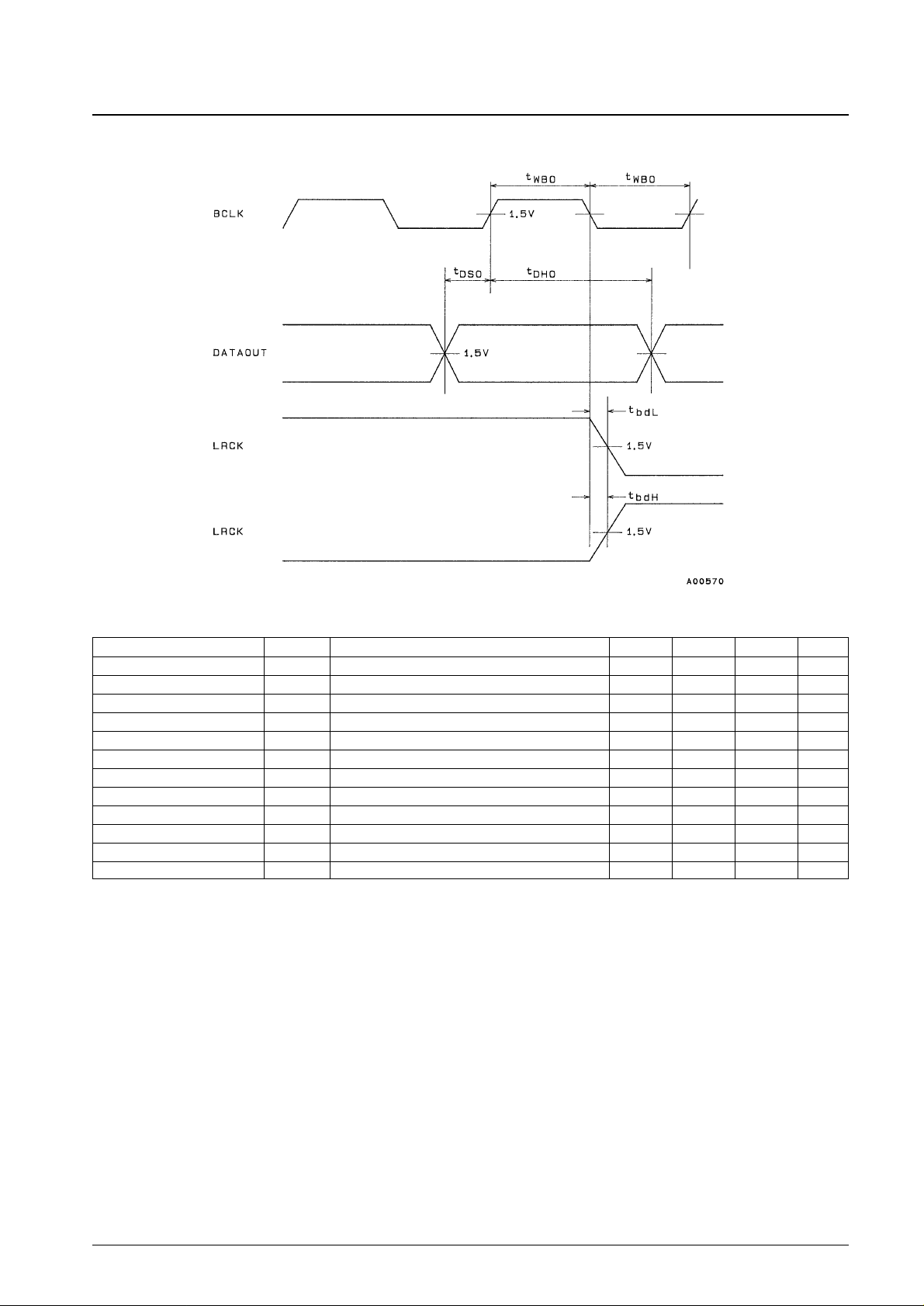
Waveforms for the AC Characteristics
Microprocessor Interface Block AC Characteristics at Ta = –30 to +75°C, VDD= 4.5 to 5.5 V
No. 4079-7/15
LC8901, 8901Q
Parameter Symbol Conditions min typ max Unit
CL low-level pulse width TWL 100 ns
CL high-level pulse Width TWH 100 ns
Data setup time TDS 50 ns
Data hold time TDH 50 ns
CL rise time Tr CL, CE, DI 30 ns
CL fall time Tf CL, CE, DI 30 ns
CE delay time TD1 1.0 µs
CL delay time TD2 50 ns
Data delay time TD3 With a 30 pF load 25 ns
CL and data delay time TD4 With a 30 pF load 50 ns
CL delay time TD5 100 ns
CL and CE delay time TD6 1.0 µs
Page 8

Waveforms for the Microprocessor Interface Block
Input mode
Output mode
Clock Modes
The LC8901 and LC8901Q support 4 clock modes selected by the XSYS and CLK pins.
1. When the CLK pin is low, the 256fs clock duty is H:L = 2:1.
2. When the CLK pin is high, the duty is 1:1.
3. Modes in which XSYS is high assume the analog source mode from the usage overview diagram.
4. The LSI automatically switches to analog source mode if there is no signal applied to the data demodulation input
pin.
5. The STOP pin controls stopping the VCO. In analog source mode, the system will not stop if the STOP pin is set
high. However, setting this pin high in digital source mode while the PLL circuit is operating will stop the system.
No. 4079-8/15
LC8901, 8901Q
XSYS pin CLK pin Mode
L L The system clock is 384fs. It is synchronized to the input data, which is then demodulated.
L H The system clock is 512fs. It is synchronized to the input data, which is then demodulated.
H L
The system clock is 384fs, but data is neither synchronized nor demodulated. The 256fs, BCLK, and LRCK signals are
output based on the crystal oscillator.
H H
The system clock is 512fs, but data is neither synchronized nor demodulated. The 256fs, BCLK, and LRCK signals are
output based on the crystal oscillator.
Page 9

LPF Pin
Setting the LPF pin high sets the PLL low-pass filter time constant to a mode in which it is automatically switched by the
PLL locking state. This pin should be set high normally.
Microprocessor Interface
The data input pin setting, output data format setting, and subcode output are controlled through the microprocessor
interface. The following item describes the interface I/O formats.
Microprocessor Interface Format
Address
Bits B0 to A3 in the format figure are the address. There are two dedicated addresses allocated, one for data input and
one for data output. Use the input address for data input and the output address for data output.
Address Codes
No. 4079-9/15
LC8901, 8901Q
Mode B0 B1 B2 B3 A0 A1 A2 A3
Data input H L H L L H H L
Data output L H H L L H H L
Page 10

Microprocessor Interface Input
1. Input pin setting
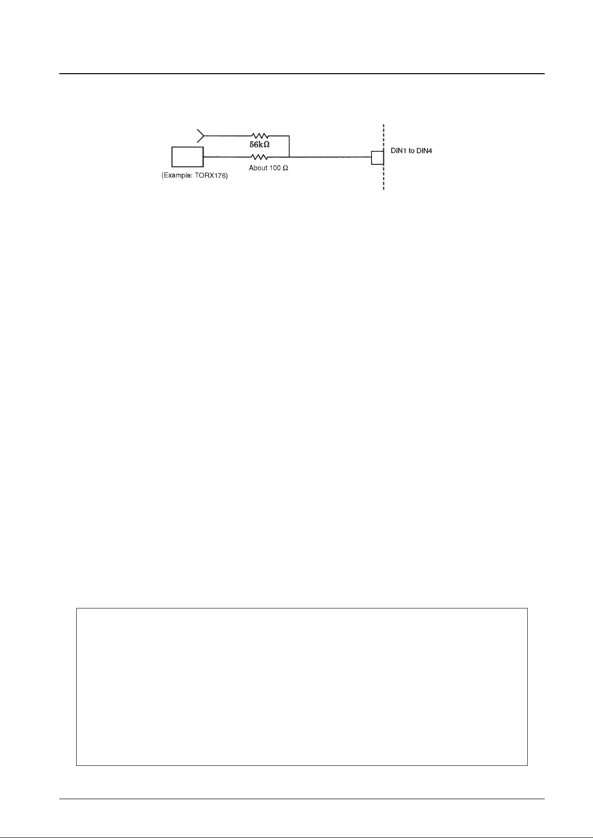
The data input pins DIN1 to DIN4 have built-in amplifiers and can receive signals from a minimum amplitude of
400 mVp-p to a maximum amplitude of VDDplus 0.3 V. Pins DIN5 and DIN6 do not have built-in amplifiers and are
only for use with optical inputs. Amplifiers must be inserted before the inputs if these pins are to be used with
coaxial input.
The data input system multiplexer is controlled by input from the microprocessor interface. The tables show the
relationship between the microprocessor interface I5 to I13 codes and the data demodulation, DOUT1, and DOUT2
signals. Bits I0 to I4 and I15 are ignored.
2. Audio data output mode setting
There are two audio data output modes, one with a 16-bit MSB first format and one with a 20-bit LSB first format.
The I14 code determines the setting.
No. 4079-10/15
LC8901, 8901Q
I5 L H L H L H L H
I6 L L H H L L H H
I7 L L L L H H H H
Data demodu-
DIN1 DIN2 DIN3 DIN4 DIN5 DIN6 GND GND
lation input
I8 L H L H L H L H
I9 L L H H L L H H
I10 L L L L H H H H
DOUT1 DIN1 DIN2 DIN3 DIN4 DIN5 DIN6 GND GND
I11 L H L H L H L H
I12 L L H H L L H H
I13 L L L L H H H H
DOUT2 DIN1 DIN2 DIN3 DIN4 DIN5 DIN6 GND GND
I14 L H
Audio data output mode 16-bit MSB first format 20-bit LSB first format
Page 11
Microprocessor Interface Output
The table lists the content of the bits D0 to D15 in the microprocessor interface format.
Interpretation of Bits D1 and D2
1. The #1 state is the state in which the data was cleared by a PLL lock error.
2. The initial settings of the modes immediately after the XMODE pin is switched from low to high are all low level.
However, D1 and D2 will indicate the #1 state.
3. The microprocessor data output registers are all cleared to 0 when PLL locking is lost. However, D1 and D2 will
indicate the #1 state.
4. The interval between two microprocessor data readout operations must be at least 6 ms. Also, when PLL locking is
lost the microprocessor must wait at least 6 ms after the error signal goes low before accessing data.
FS Code
The SUB1 and SUB2 pins indicate the input data sampling frequency.
The #1 state is the state in which the data was cleared by a PLL lock error.
Lock and Errors
1. LOCK pin: This pin goes high when preamble detection has succeeded for 2 consecutive frames and thus indicates
the PLL locked state. This pin is low at all other times. In particular, it is low when the XMODE pin is low, when the
STOP pin is high, and in analog source mode.
2. ERROR pin: Goes high when an error exists in the input data or when the PLL circuit is in the unlocked state. When
the data returns to normal it holds the high level for about 200 to 300 ms and then falls to low. This period is
inversely proportional to the input data sampling frequency. This pin is high when the XMODE pin is low, when the
STOP pin is high, and in analog source mode.
3. Data processing when errors occur: The table below lists the data processing that is performed when an error occurs.
Note: The term “C bit data” means data that was decoded from the channel status bit.
• When there is no data input to the data demodulation system, the system automatically switches from PLL
operation to the crystal oscillator and enters analog source mode.
• These pins indicate a state identical to a PLL lock error in any of the following cases: The STOP pin is high, the
XMODE pin is low, or the system is in analog source mode.
No. 4079-11/15
LC8901, 8901Q
Bit Meaning
D0 Invalid bit. A low level is always output.
D1 Indicate the sampling frequency.
D2 Correspond to the 2 external output port pins.
D3
Indicates the copy flag.
Low: copy protected, high: copying allowed.
D4 Outputs the first bit in the channel status bits.
D5 to D12 These bits serially output the 8 bits of the channel status category code.
D13 D15 Invalid bit. A low level is always output.
Sampling frequency 32 kHz 44.1 kHz 48 kHz #1
D1 H L L H
D2 H L H L
Sampling frequency 32 kHz 44.1 kHz 48 kHz #1
SUB1 H L L H
SUB2 H L H L
Error type Audio output data C bit output data
Continuous parity errors for up to 8 cycles The previous data value is output Held
Continuous parity errors for 9 or more cycles All zero data is output Held
PLL lock error All zero data is output Data is cleared and the #1 state is indicated.
Page 12

PLL
1. The VCO is formed from a ring oscillator.
2. PLL operation starts when correct data is input to the data demodulation system and the XMODE pin goes high.
3. The low-pass filter time constant can be automatically switched according to the PLL lock state by setting the LPF
pin high.
4. To prevent PLL locking failures, if a PLL locking operation is started and the PLL does not lock within a fixed
period, reinitialize the PLL system, and start the PLL locking operation again.
5. PLL operation is forcibly stopped by setting the STOP pin high. Normal operation will start again if the pin is set
low.
XMODE Pin
The XMODE pin resets the system. Normal system operation is started by setting this pin high after the power supply
voltage has risen to at least 4.5 V. If the XMODE pin is set low, the VCO free-running clock is output from the FS384
pin and the internal circuits are reset.
Power-on Sequence Diagram
1. No input pins should be accessed until the XMODE pin has gone high and the system has started to operate.
2. The microprocessor interface pins must not be accessed until the XMODE pin has gone high and the system has
started to operate.
3. The data output pins must not be accessed until the ERROR pin has gone low after the XMODE pin has gone high.
No. 4079-12/15
LC8901, 8901Q
Page 13

Data Output Timing
The figure below shows the data output timing.
1. Data is output in synchronization with the falling edge of the BCLK signal.
2. Data, BCLK, and LRCK are output in synchronization with the rising edge of the 256fs clock.
Timing Chart
No. 4079-13/15
LC8901, 8901Q
Page 14
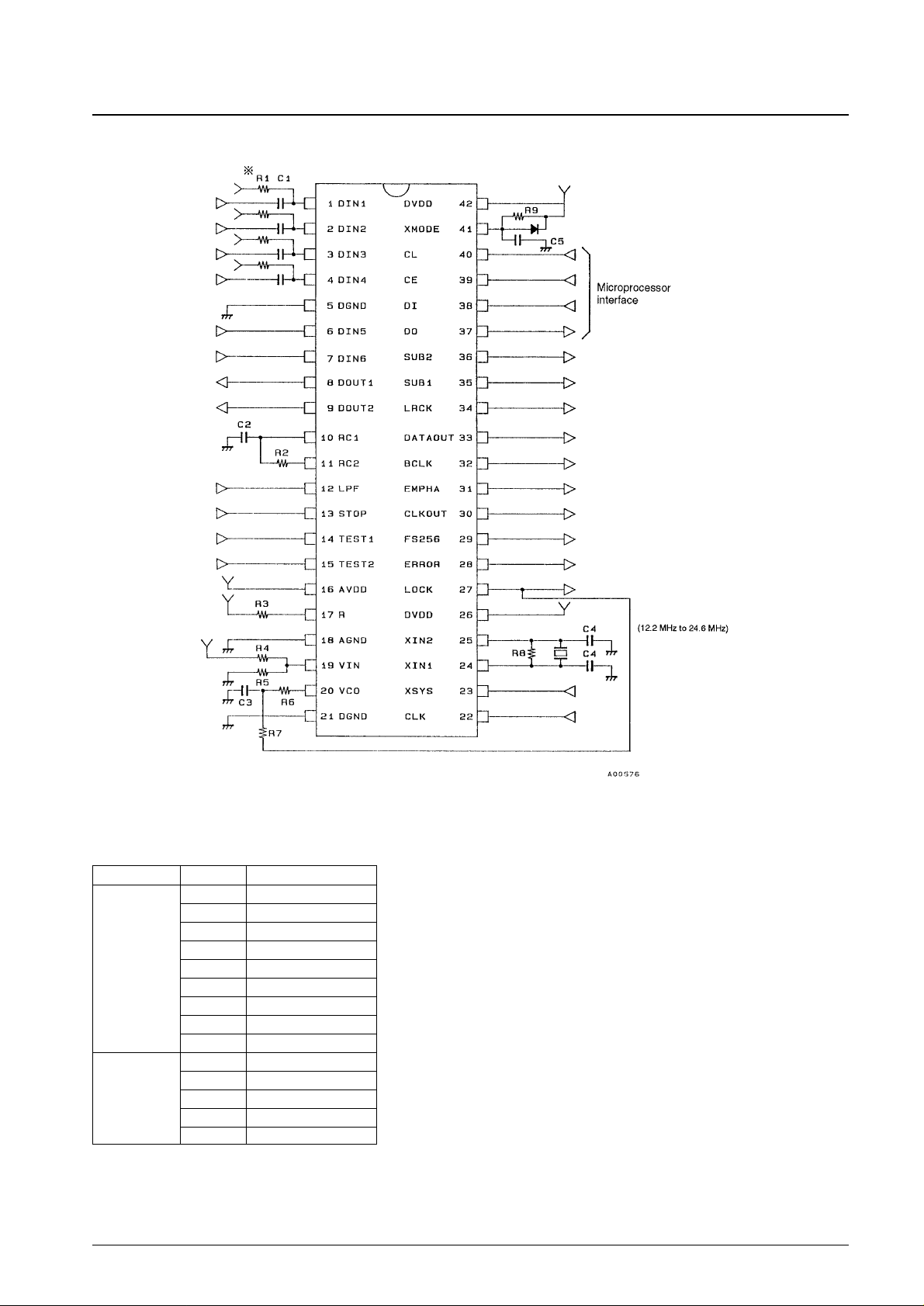
Sample Application Circuit
Note: All input pin resistors and capacitors are the same.
Recommended Constants for the Application Circuit
Note: * The constants listed above are for applications that connect to the input pins using coaxial cable. If connection is through an optical receiver
module, remove the C1 capacitors and use 56 kΩ resistors for R1.
Note that DIN5 and DIN6 are only for use with optical receiver modules.
No. 4079-14/15
LC8901, 8901Q
Item Symbol Constant value
R1 330 kΩ*
R2 33 kΩ
R3 24 kΩ
R4 5.1 kΩ
Resistors R5 5.1 kΩ
R6 150 Ω
R7 180 kΩ
R8 200 kΩ
R9 10 kΩ
C1 0.1 µF*
C2 1000 pF
Capacitors C3 0.01 µF
C4 10 pF to 47 pF
C5 10 µF to 100 µF
Page 15
No. 4079-15/15
LC8901, 8901Q
Sample Optical Receiver Module Circuit
This catalog provides information as of February, 1997. Specifications and information herein are subject to
change without notice.
■ No products described or contained herein are intended for use in surgical implants, life-support systems, aerospace
equipment, nuclear power control systems, vehicles, disaster/crime-prevention equipment and the like, the failure of
which may directly or indirectly cause injury, death or property loss.
■ Anyone purchasing any products described or contained herein for an above-mentioned use shall:
➀ Accept full responsibility and indemnify and defend SANYO ELECTRIC CO., LTD., its affiliates, subsidiaries and
distributors and all their officers and employees, jointly and severally, against any and all claims and litigation and all
damages, cost and expenses associated with such use:
➁ Not impose any responsibility for any fault or negligence which may be cited in any such claim or litigation on
SANYO ELECTRIC CO., LTD., its affiliates, subsidiaries and distributors or any of their officers and employees
jointly or severally.
■ Information (including circuit diagrams and circuit parameters) herein is for example only; it is not guaranteed for
volume production. SANYO believes information herein is accurate and reliable, but no guarantees are made or implied
regarding its use or any infringements of intellectual property rights or other rights of third parties.
 Loading...