

Page 1
CMOS LSI
Ordering number : EN4128B
83096HA (OT)/7062JN No. 4128-1/12
SANYO Electric Co.,Ltd. Semiconductor Bussiness Headquarters
TOKYO OFFICE Tokyo Bldg., 1-10, 1 Chome, Ueno, Taito-ku, TOKYO, 110 JAPAN
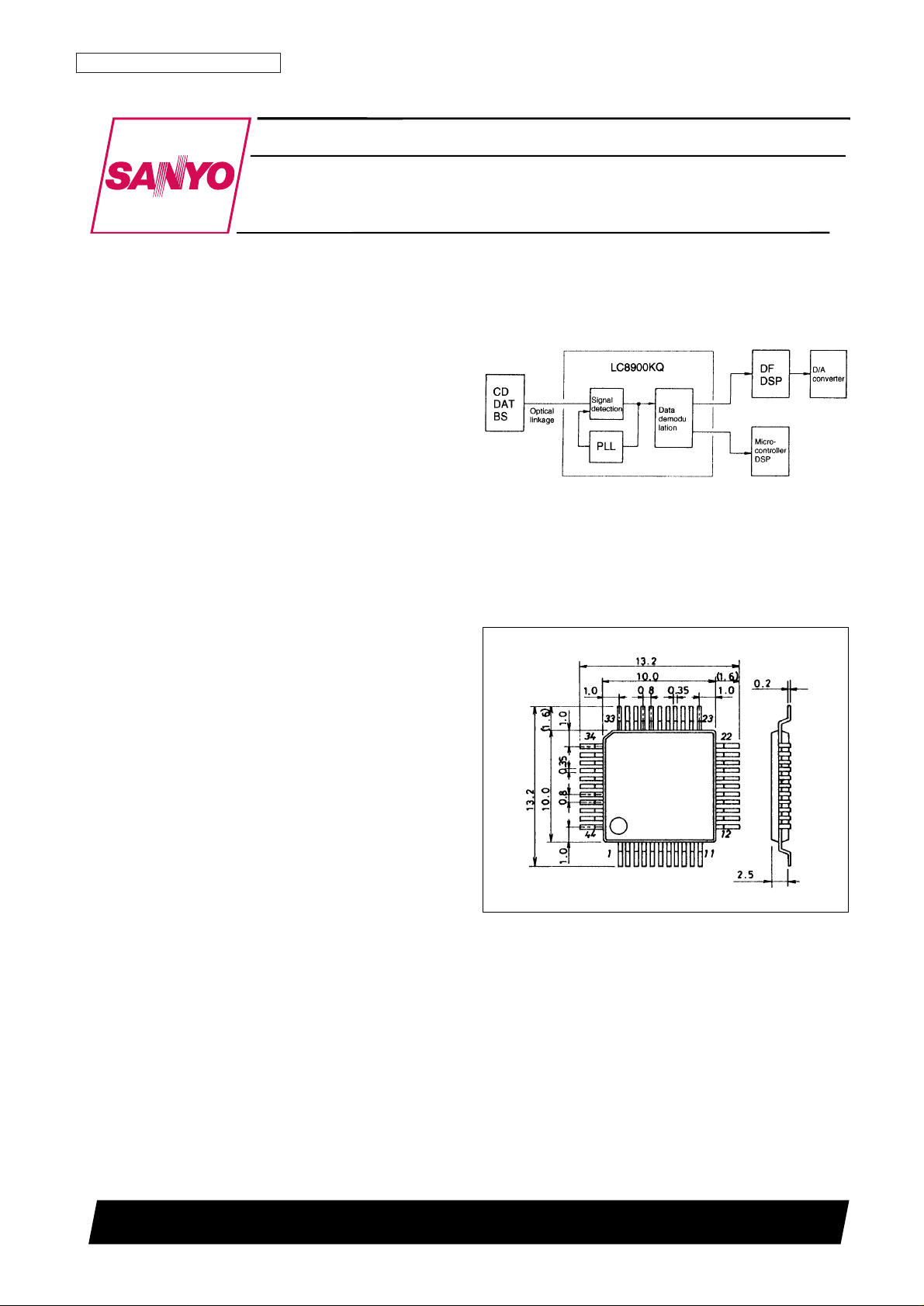
Digital Audio Interface Receiver
LC8900KQ
Overview
The LC8900KQ is a CMOS LSI circuit chip that can be
used to enable the EIAJ CP-1201 formatted data
transmission between digital audio equipment. It is used
by the receiving end and operates synchronously with
input signals. This chip demodulates input signals into
normally-formatted signals.
Features
• On-chip PLL circuit: enables the LSI operation to be
synchronous to the transmitted EIAJ format input
signals.
• Four input pins and one output pin: The output pin
enables the input data to be sent as they are.
• Two data output function modes: 20-bit data LSB first
mode and 16-bit data MSB first mode.
• Four output clocks: Bit clock, LRCK, 384Fs and 256Fs.
All these clocks are synchronized to the data.
• Various signal outputs: copy inhibit, emphasis on:off
control, user’s bit, validity flag and sampling frequency.
• LPF time constant select mode: This function can be
used in the PLL lock-up state.
• Error detect signal output: If an input data error is
detected, this LSI circuit chip outputs the error signal.
In this case, the previous data will be output by the chip.
• Lock-up signal output: This signal is output when the
internal PLL (Phase Locked Loop) block of the LSI
circuit chip is locked.
• The chip has the pin to receive a signal for stopping the
PLL operation.
• Control and processing mode via microcontroller
interface: input pin select, copy information and
sampling frequency output.
• Each input pin has an internal amplifier circuit.
• Si gate, CMOS process technology and single 5V power
supply applicational and functional concept.
Applicational and Functional Concept
Package Dimensions
unit:mm
3148-QFP44MA
Preliminary
SANYO: QIP44MA
[LC8900KQ]
Page 2
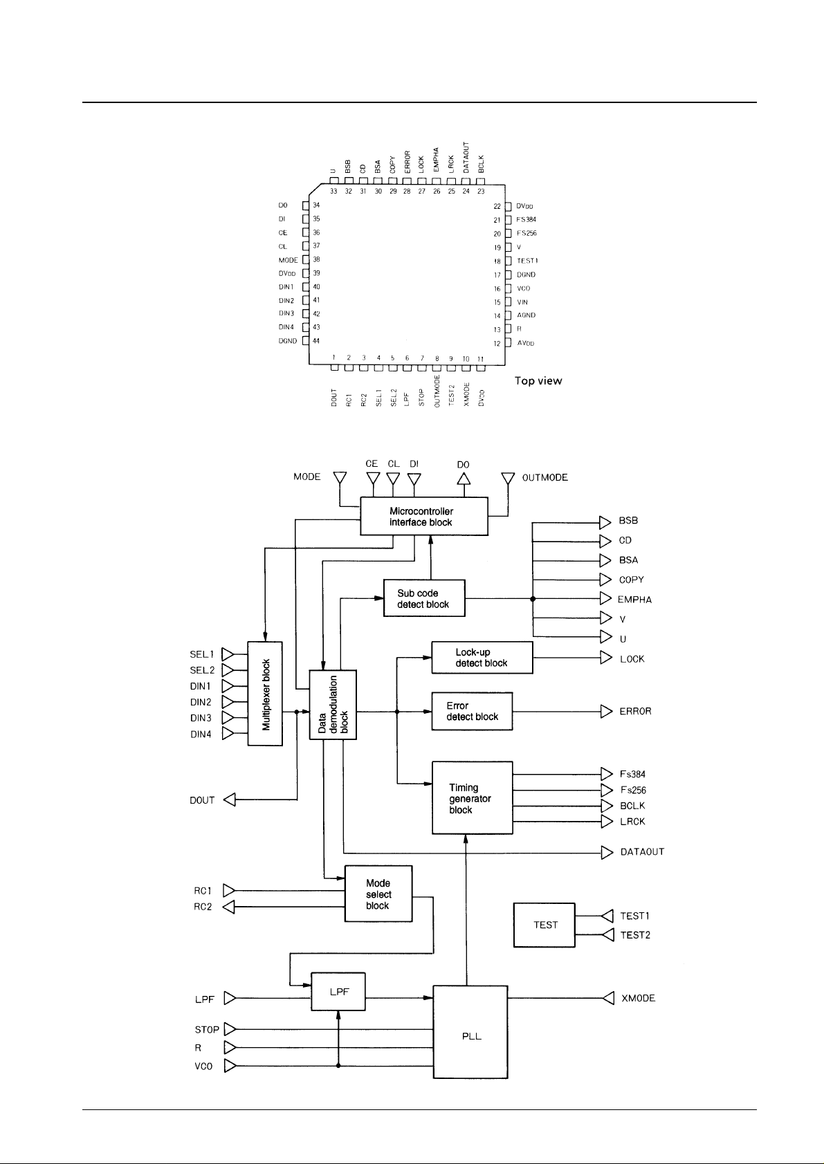
Pin Assignment
Block Diagram
No. 4128-2/12
LC8900KQ
Page 3
Pin Functions
No. 4128-3/12
LC8900KQ
Pin No. Pin Name I/O Type Functional Description
1 DOUT O Input data output pin. However, its output is fixed at the low level if the DIN4 input pin is selected.
2 RC1 I RC oscillation pin
3 RC2 O RC oscillation pin
4 SEL1 I Input pin select pin
5 SEL2 I Input pin select pin
6 LPF I High level = LPF time constant select mode. low level = LPF time constant fixed mode. Fixed to high in most cases.
7 STOP I High = level:Forces the VCO operation to stop. Fixed to low in most cases.
I Output data format select pin.
8 OUTMODE High = 20-bit LSB first data format.
Low = 16-bit MSB first data format
9 TEST2 I Test pin:Connected to the DGND in most cases.
10 XMODE I Input pin to start the PLL operation immediately after the LSI chip is powered on.
11 DV
DD
Digital power supply
12 AV
DD
Analog power supply
13 R I VCO oscillation bandwidth adjust pin
14 AGND Analog ground
15 Vin I VCO self oscillation frequency setting pin
16 VCO O PLL LPF pin
17 DGND Digital Ground
18 TEST1 I Test pin:Connected to the DGND in most cases.
19 V O Validity flag output pin
20 FS256 O 256 Fs clock output pin
21 FS384 O 384 Fs clock output pin
22 DV
DD
Digital Power Supply
23 BCLK O Bit clock output pin
24 DATAOUT O Audio data output pin
25 LRCK O L/R clock output pin, Lch = high, Rch = low
26 EMPHA O Emphasis control (on/off) output pin:High = emphasis mode. Low = none-emphasis mode.
27 LOCK O PLL lock state output pin:High = PLL locked state. Low = PLL unlocked state.
28 ERROR O Input data error detect signal output:High = error detected.
29 COPY O Copy information output pin
30 BSA O Input data sampling frequency indication:High = 2 kHz.
31 CD O Input data sampling frequency indication:High = 44.1 kHz.
32 BSB O Input data sampling frequency indication:High = 48kHz.
33 U O User’s bit output pin
34 DO O Microcontroller interface output pin
35 DI I Microcontroller interface input pin
36 CE O Microcontroller interface chip enable input pin
37 CL O Microcontroller interface clock input pin
38 MODE I
Microcontroller interface control input:High = microcontroller interface active mode.
Low = microcontroller interface inactive mode.
39 DV
DD
Digital power supply
40 DIN1 I Data input pin
41 DIN2 I Data input pin
42 DIN3 I Data input pin
43 DIN4 I Data input pin
44 DGND Digital ground
Page 4
Specifications
Absolute Maximum Ratings at Ta = 25°C
Allowable Operating Range at Ta = –30°C to +75°C
DC Characteristics at Ta = –30 to +75°C, VDD= 4.5 V to 5.5 V
AC Characteristics at Ta = –30 to 75°C, VDD= 4.5 to 5.5 V
Note 1: All input pins except DIN1, DIN2, DIN3, DIN4 and XMODE.
Note 2: XMODE pin
Note 3: VDD=5.0V, Ta = 25 °C, input Fs=48 kHz.
Note 4: Before DIN1 to DIN4 input capacity is exceeded.
No. 4128-4/12
LC8900KQ
Parameter Symbol Conditions Ratings Unit
Maximum supply voltage V
DD
max Ta = 25°C –0.3 to +7.0 V
Input/output voltage V
I
· VOTa = 25°C –0.3 to V
DD
+0.3 V
Ambient operating temperature Topr –30 to +75 °C
Ambient storage temperature Tstg –55 to +125 °C
Parameter Symbol Conditions min typ max Unit
Supply voltage V
DD
4.5 5.0 5.5 V
Parameter Symbol Conditions min typ max Unit
Input high level voltage V
IH
*1 2.2 V
DD
+ 0.3 V
Input low level voltage V
IL
*1 –0.3 0.8 V
Input high level voltage V
IH
*2 0.8 V
DD
V
DD
+ 0.3 V
Input low level voltage V
IL
*2 –0.3 0.2 V
DD
Output high level voltage V
OH
IOH= –1 µA V
DD
– 0.05 V
Output low level voltage V
OL
IOL= 1 µA V
SS
+ 0.05 V
Current drain I
DD
*3 11 12 mA
Input amplitude V
IN
*4 0.4 V
DD
+ 0.3 V
P-P
Parameter Symbol Conditions min typ max Unit
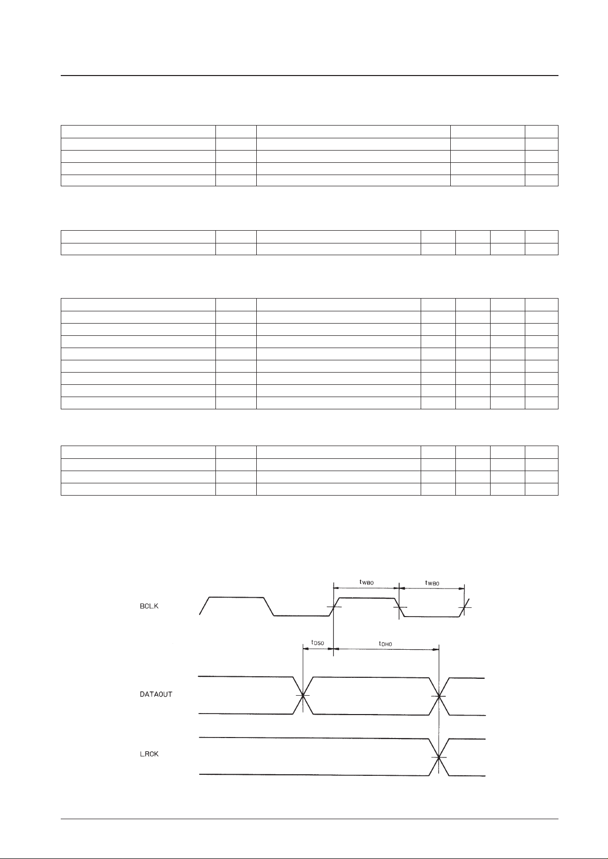
Output pulse width t
WBO
Fs = 48kHz 160 ns
Output set-up time t
DSO
80 ns
Output data hold time t
DHO
80 ns
Page 5

AC Characteristics at the Microcontroller Interface Block at Ta = –30 to +75°C, VDD= 4.5V to 5.5V
AC Characteristics at the Microcontroller Interface Block
No. 4128-5/12
LC8900KQ
Parameter Symbol Conditions min typ max Unit
CL low pulse width TWL 100 ns
CL high pulse width TWH 100 ns
Data set up time TDS 50 ns
Data hold time TDH 50 ns
CL rise time Tr CL, CE, DI 30 ns
CL fall time Tf CL, CE, DI 30 ns
CE delay time TD1 1.0 µs
CL delay time TD2 50 ns
Data delay time TD3 Load capacitance = 30 pF 25 ns
CL/data delay time TD4 Load capacitance = 30 pF 50 ns
CL delay time TD5 100 ns
CL/CE delay time TD6 1.0 µs
Page 6

PLL VCO Functional Circuit Block
VCO
• The VCO (Voltage Controlled Oscillator) functional block consists of multiple ring oscillator ad shown above.
• The ring oscillator produces the frequencies from 3 MHz to 40 MHz according to the VCO pin voltages 0 V to 3 V.
• The VCO self oscillation frequency is determined by the VIN pin voltage.
Phase Detector
• The phase detector circuit operates on the rising edge of the incoming signals. It compares the clock generated from
the input signal with the VCO clock.
LPF (Low-pass filter)
• The charge pump and the LPF are shown above. The LPF time constant varies depending on the lock judge signal.
No. 4128-6/12
LC8900KQ
Page 7

DATA
(1) The relationship between the data input pins and the data select pins are shown in the table below.
• Each input pin has an internal amplification circuit. Therefore the signal with the amplitude of 400 m V
P-P
up to
VDD+0.3 V can be input to this LSI chip. However, in the case of coaxial cable or optical module input the application
will change as the sample application circuit shown later.
• Connect to the unused input pin to the GND or VDD.
(2) The relationship between the OUTMODE pin and the two output data formats is shown in the table below.
• IF an error is detected in an input data, that input data is not output. Instead, the previous data will be output.
• The data output is synchronized with falling edge of the bit clock.
• IF the PLL is in the Lock state, the 384 Fs or 256 Fs clock that is synchronized with the output data will be output.
Note that the duty is of the 256 Fs clock is 'H:L = 2:1'. It is not 'H:L = 1:1'.
Sub Codes
The sub code output consists of the copy inhibit signal, emphasis mode signal, sampling frequency signal, validity flag
signal and user’s bit. The table below details these sub code outputs.
Clock Modes
The control clock is specified by the VCO. The VCO has two modes: self oscillation mode and PLL mode as shown
below.
• When the STOP pin is changed to the high level, the PLL functional circuit block stops its operation and the entire
circuit operation is then forced to stop. The entire circuit will start the normal operation again when the STOP pin is
changed to the low level.
• If the LOCK operation is not activated in a certain fixed time period after the PLL enters the lock-up state:
Reinitialize the PLL functional circuit block to active the lock-up mode. This should be done to prevent the PLL lock
error.
No. 4128-7/12
LC8900KQ
COPY inhibit signal COPY pin level = high:Copy not inhibited.
COPY pin level = low:Copy inhibited.
Emphasis mode signal EMPHA pin level = high:Emphasis mode.
EMPHA pin level = low:Non emphasis mode.
BSA pin level = high:32 kHz sampling frequency
Sampling frequency CD pin level = high:44.1 kHz sampling frequency
BSB pin level = high:48 kHz sampling frequency
Validity flag signal This signal is output from the V pin in sub frame unit.
User’s bit This signal is output from the U pin in sub frame unit.
Self oscillation mode
• XMODE pin level=low • The VCO continues its oscillation according to the VIN pin potential. BCLK,
LRCK, and FS256 clocks are not effective.
• No data input • The VCO continues its oscillation according to the VIN pin potential. FS384,
BCLK, LRCK, and FS256 clocks output.
PLL mode • Data input with the XMODE pin level=high • The PLL block and the entire circuit are in the normal operation state.
SEL1 SEL2 DOUT
DIN1 L L DIN1 data output
DIN2 L H DIN2 data output
DIN3 H L DIN3 data output
DIN4 H H low level signal output
(fixed level output)
OUTMODE pin
H 20-bit LSB first data output format
L 16-bit MSB first data output format
Page 8

Microcontroller Interface
The microcontroller interface function can be used by setting the MODE pin level to high. In this function mode, the
pins CE, CL, DI and DO can be used to allow the interface between the LSI chip and a microcontroller. This
microcontroller interface allows the microcontroller to control and process the input pin selection output data format,
copy information and sampling frequency output.
Set the mode CE, CL, and DI pins to the low when the microcontroller interface is not used.
Input data format
Output data format
Bits B0 to A3 of the DI signal in the format figures on the preceding page are used to specify an 8-bit address. These 8bits are used to specify the addresses both in the input and output operations.
(1) Data input mode
Bits DI0 to DI4 of the DI signal are used to select the operation modes shown in the tables below.
• When the MODE pin level is set to high, the input pins and output data format are selected by the microcontroller.
This means that the selection data input to the SEL1, SEL2 and OUTMODE pins has no significance.
Just after the XMODE pin is changed to high from low, DI0 to DI4 are set to low.
No. 4128-8/12
LC8900KQ
B0 B1 B2 B3 A0 A1 A2 A3
Data input mode 1 0 1 0 0 1 1 0
Data output mode 0 1 1 0 0 1 1 0
DI2 DI3 input pin selection DOUT
L L DIN1 DIN1 data output
L H DIN2 DIN2 data output
H L DIN3 DIN3 data output
H H DIN4 low level signal output (fixed level output)
DI1 = L 16-bit data MSB first output mode
DI1 = H 20-bit data LSB first output mode
Page 9

(2) Data output mode
Bits DO0 to DO4 of the DO signal have the following meanings show in the tables below.
• 6 ms or longer is required to read data after the ERROR pin is changed to L. Take at least 6 ms between data read out.
Any codes when DO1 is high and DO2 is low is invalid in other conditions than this.
Timing Chart
No. 4128-9/12
LC8900KQ
DO1 DO2 Sampling frequency selection
L L 44.1 kHz
L H 48 kHz
H H 32 kHz
DO3 = L Copy inhibited
DO3 = H Copy not inhibited
Page 10

LOCK and ERROR Pins
Descriptions of LOCK and ERROR pins are as follows.
LOCK: Preamble detector. When two or more preambles are detected successively, this pin outputs high level signal.
When XMODE pin is low or STOP pin is high or no signal input, outputs low level signal.
ERROR: When two or more preambles are not detected successively, or 8 subframes’ continuous results of parity check
are not accomplished, this pin outputs high level signal to indicate system error. When XMODE pin is low or
STOP pin is high or no signal input, outputs high level signal.
1. Output pin conditions when error occurs.
Note 1: When input pin goes to no input signal, errors can be caused due to the timing of turning into no input signal. Take the same operation as parity
error in this case.
2: When error occurring, the outputs pin’s change synchronizes the timing of ERROR pin’s turning into the high level. When XMODE pin is set to low
or STOP pin is to high, ERROR pin goes to high at the same time and the other output pins will change as in the table above.
2. Error signals and read out timing
After the ERROR pin goes to low, each data will be able to be accessed after the next clock pulse.
XMODE Pin
XMODE pin resets the system. This pin must be turned into high after 4.5 V or more power is applied to start the system
normally. By setting XMODE pin to low, VCO self oscillation frequency from FS384 pin will reset the internal circuit.
Power rise diagram
Each input pin will be accessible after XMODE turns to be on to start the system.
Microcontroller interface pins will be accessible after XMODE turns to be on to start the system.
Each data output pin will be accessible after XMODE turns to be on and ERROR pin goes to low. COPY, EMPHA, CD,
BSA, and BSB cords will be accessible at least 6 ms later after ERROR pin goes to low.
No. 4128-10/12
LC8900KQ
STOP is low
Keeps the value just
before the STOP goes to
high.
Outputs low level signal.
No effect by error.
Parity error
Outputs preceding data.
Outputs low level signal
after reset.
No effect by error.
No input signal
Outputs the indeterminate
data. *1
Outputs the indeterminate
data. *1
No effect by error.
Output pin
DATAOUT
V
U
CD, BSA
BSB, COPY
EMPHA
DOUT
DATAOUT, V, U Accessible as soon as ERROR pin goes to low
CD, BSA, BSB, COPY, EMPHA Accessible 6 ms or later after ERROR pin goes to low
XMODE is low
Keeps the indeterminate
condition of high or low.
Outputs low level signal.
No effect by error.
Page 11

Sample Application Circuit
∗ Apply the power to AVDDand two DVDDs simultaneously, or a latch up will occur.
∗ The allowable current to BSA, CD, and BSB pins is 8 mA.
No. 4128-11/12
LC8900KQ
Page 12

No. 4128-12/12
LC8900KQ
Recommended External Components
*: This is a value when coaxial cables are connected to the
input pins. Take C1 and replace R1 with a 56 kΩ resistor
if optical cables are connected instead of coaxial cables.
Connection to an Optical Module
This catalog provides information as of November, 1997. Specifications and information herein are subject to
change without notice.
■ No products described or contained herein are intended for use in surgical implants, life-support systems, aerospace
equipment, nuclear power control systems, vehicles, disaster/crime-prevention equipment and the like, the failure of
which may directly or indirectly cause injury, death or property loss.
■ Anyone purchasing any products described or contained herein for an above-mentioned use shall:
➀
Accept full responsibility and indemnify and defend SANYO ELECTRIC CO., LTD., its affiliates, subsidiaries and
distributors and all their officers and employees, jointly and severally, against any and all claims and litigation and all
damages, cost and expenses associated with such use:
➁
Not impose any responsibility for any fault or negligence which may be cited in any such claim or litigation on
SANYO ELECTRIC CO., LTD., its affiliates, subsidiaries and distributors or any of their officers and employees
jointly or severally.
■ Information (including circuit diagrams and circuit parameters) herein is for example only; it is not guaranteed for
volume production. SANYO believes information herein is accurate and reliable, but no guarantees are made or implied
regarding its use or any infringements of intellectual property rights or other rights of third parties.
Component type Component code Value
R1 330 kΩ*
R2 33 kΩ
R3 10 kΩ
R4 24 kΩ
Resistor R5 5.1 kΩ
R6 5.1 kΩ
R7 150 Ω
R8 180 kΩ
R9 330 Ω
C1 0.1 µF
Capacitor
C2 1000 pF
C3 10 µF to 100 µF
C4 0.01 µF
 Loading...