

Page 1
11901 RM (IM) SK No.6842-1/24
Ver.1.00
N2599
Preliminary
Overview
The LC8772C8B, LC8772B2B LC877296B and LC877280B are 8 bit single chip microcontrollers with the following
on-chip functional blocks :
- CPU: operable at a minimum bus cycle time of 100 ns
- On-chip ROM Maximum Capacity : LC8772C8B 128K bytes
LC8772B2B 112K bytes
LC877296B 96K bytes
LC877280B 80K bytes
- On-chip RAM capacity: 2048 bytes
- LCD controller / driver
- 16 bit timer / counter (can be divided into two 8 bit timers)
- 16 bit timer / PWM (can be divided into two 8 bit timers)
- Timer fo r use as date / time clock
- Synchronous serial I/O port (with automatic block transmit / receive function)
- Asynchronous / synchronous serial I/O port
- 12-channel × 8-bit AD converter
- Small signal detector
- 14-source 10-vectored interrupt system
All of the above functions are fabricated on a single chip.
Features
(1) Read-Only Memory (ROM)
- 131072 × 8bits (LC8772C8B)
- 114688 × 8bits (LC8772B2B)
- 98304 × 8bits (LC877296B)
- 81920 × 8bits (LC877280B)
(2) Random Access Memory (RAM): 2048 × 9 bits (LC8772C8B, LC8772B2B, LC877296B, LC877280B )
(3) Minimum Bus Cycle Time: 100 ns (10 MHz)
Note: The bus cycle time indicates ROM read time.
(4) Minimum Instruction Cycle Time: 300 ns (10MHz)
8-Bit Single-Chip Microcontroller
LC8772C8B/B2B/96B/80B
Ordering number : ENN*6842
CMOS IC
Page 2

LC8772C8B/B2B/96B/80B
No.6842-2/24
(5) Ports
- Input/output ports
Data direction programmable for each bit individually : 26 (P1n, P30-P35, P70-P7 3, P 8n)
Data direction programmable in nibble units : 8 (P0n)
(When N-channel open drain output is selected, data can be input in bit units.)
- Input ports : 2 (XT1,XT2)
- LCD ports
Segment output : 48 (S00-S47)
Common output : 4 (COM0-COM3)
Bias terminals fo r LC D d river 3 (V1-V3)
Other functions
Input/output ports : 48(PAn,PBn,PCn,PDn,PEn,PFn)
Input ports : 7 (PLn)
- Oscillator pins : 2 (CF1,CF2)
- Reset pin : 1 (
RES
)
- Power supply : 6 (VSS1-3,VDD1-3)
(6) LCD controller
- Seven display modes are available (static, 1/2, 1/3, 1/4 duty × 1/2, 1/3 bias)
- Segment output and common output can be switched to general purpose input/output ports.
(7) Small signal detection (MIC signals etc)
- Counts pulses with the level which is greater than a preset value
- 2 bit counter
(8) Timers
- Timer 0: 16 bit timer / counter with capture register
Mode 0: 2 channel 8-bit timer with programmable 8 bit prescaler and 8 bit capture register
Mode 1: 8 bit timer with 8 bit programmable prescaler and 8 bit capture register + 8 bit
Counter with 8-bit capture register
Mode 2: 16 bit timer with 8 bit programmable prescaler and 16 bit capture register
Mode 3: 16 bit counter with 16 bit capture register
- Timer 1: PWM / 16 bit timer with toggle output function
Mode 0: 2 channel 8 bit timer (with toggle output)
Mode 1: 2 channel 8 bit PWM
Mode 2: 16 bit timer (with toggle output) Toggle output from lower 8 bits is also possible.
Mode 3: 16 bit timer (with toggle output) Lower order 8 bits can be used as PWM.
- Base Timer
1) The clock signal can be selected from any of the following :
Sub-clock (32.768kHz crystal oscillator), system clock, and prescaler output from timer 0
2) Interrupts of five different time intervals are possible.
(9) Serial-interface
- SIO 0: 8 bit synchronous serial interface
1) LSB first / MSB first is selectable
2) Internal 8 bit baud-rate generator (fastest clock period 4 / 3 Tcyc)
3) Consecutive automatic data communication (1-256 bits)
- SIO 1: 8 bit asynchronous / synchronous serial interface
Mode 0: Synchronous 8 bit serial IO (2-wire or 3-wire, transmit clock 2–512 Tcyc)
Mode 1: Asynchronous serial IO (half duplex, 8 data bits, 1 stop bit, baud rate 8–2048Tcyc)
Mode 2: Bus mode 1 (start bit, 8 data bits, transmit clock 2–512 Tcyc)
Mode 3: Bus mode 2 (start detection, 8 data bits, stop detection)
(10) AD converter
-8 bits × 12 channels
Page 3
LC8772C8B/B2B/96B/80B
No.6842-3/24
(11) Re mo te control receiver circuit (connecte d to P73 / INT3 / T0 IN terminal)
-Noise rejection function (noise rejection filter’s time constant can be selected from 1 / 32 / 128 Tcyc)
(12) Watchdog timer
- The watching time period is determined by an external RC.
- Watchdog timer can produce interrupt or system reset
(13) Interrupts: 14 sources, 10 vectors
1) Three prior ity (low, high and highest) multiple interrupts are supporte d . During interrupt handl ing, an equal or
lower priority interrupt request is postponed.
2) If interrupt requests to two or more vector addresses occur at once, the higher priority interrupt takes precedence.
In the case of equal priority levels, the vector with the lowest address takes precedence.
No. Vector Selectable Level Interrupt signal
1 00003H X or L INT0
2 0000BH X or L INT1
3 00013H H or L INT2/T0L
4 0001BH H or L INT3/Base timer
5 00023H H or L T0H
6 0002BH H or L T1 L/T1H
7 00033H H or L SIO0
8 0003BH H or L SIO1
9 00043H H or L ADC/MIC
10 0004BH H or L Port 0
• Priority Level : X > H > L
• For equal prio rity levels, vector with lowest address takes precedence.
(14) Subroutine stack levels: 1024 levels max. Stack is located in RAM.
(15) Multiplication and division
- 16 bit × 8 bit (executed in 5 cycles)
- 24 bit × 16 bit (12 cycles)
- 16 bit ÷ 8 bit (8 cycles)
- 24 bit ÷ 16 bit (12 cycles)
(16) Oscillation circuits
- On-chip RC oscillation for system clock use.
- CF oscillation for system clock us e. (R f bu ilt in, Rd external)
- Crystal oscillation low speed system clock use. (Rf built in, Rd external)
(17) Standby function
- HALT mode
HALT mode is used to reduce power consumption. During the HALT mode, program execution is stopped but
peripheral circuits keep operating (some parts of serial transfer operation stop.)
1) Oscillation circuits are not stopped automatically.
2) Released by the system reset or interrupts.
-HOLD mode
HOLD mode is used to reduce power consumption. Program execution and peripheral circuits are stopped.
1) CF, RC and crystal oscillation circuits stop automatically.
2) Released by any of the following conditions.
(1) Low level input to the reset pin
(2) Specified level input to one of INT0, INT1, INT2
(3) Port 0 interrupt
Page 4

LC8772C8B/B2B/96B/80B
No.6842-4/24
-X’tal HOLD made
X’tal HOLD mode is used to reduce power consumption. Program execution is stopped.
All peripheral circuits except the base timer are st opped.
1) CF and RC oscillation circuits stop automatically.
2) Crystal oscillator operation is kept in its state at HOLD mode inception.
3) Released by any of the following conditions
(1) Low level input to the reset pin
(2) Specified level input to one of INT0, INT1, INT2
(3) Port 0 interrupt
(4) Base -timer inter r upt
(18) Package
- QIP100E
- SQFP100
(19) Development tools
- Evaluation chip : LC876096
- Emulator: EVA62S + ECB876500 (Evaluation chip board) + SUB877200 + POD100QFP
or POD100SQFP (Type B)
- Flash ROM version: LC87F72C8A
Page 5
LC8772C8B/B2B/96B/80B
No.6842-5/24
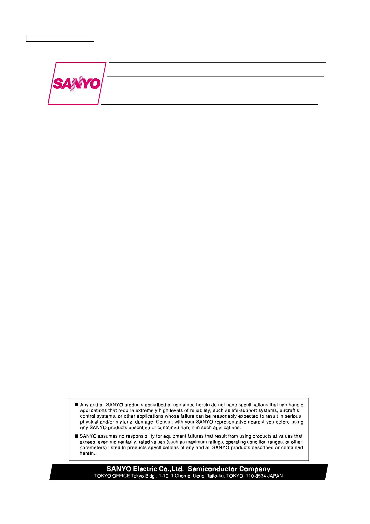
Pin Assignment
SANYO: QIP100E
S20/PC4
S19/PC3
S18/PC2
S17/PC1
S16/PC0
S15/PB7
S14/PB6
S13/PB5
S12/PB4
S11/PB3
S10/PB2
S9/PB1
S8/PB0
S7/PA7
S6/PA6
S5/PA5
S4/PA4
S3/PA3
S2/PA2
S1PA1
V2/PL5
V1/PL4
COM0/PL0
COM1/PL1
COM2/PL2
COM3/PL3
P30
P31
VSS3
VDD3
P32
P33
P34
P35
P00
P01
P02
P03
P04
P05
P06
P07
P10/SO0
P11/SI0/SB0
P12/SCK0
P13/SO1
P14/SI1/SB1
P15/SCK1
P16/T1PWML
P17/T1PWMH/BU
Z
RES
XT1/AN10
XT2/AN11
VSS1
CF1
CF2
VDD1
P80/AN0
P81/AN1
P82/AN2
P83/AN3
P84/AN4
P85/AN5
P86/AN6
P87/AN7/MICIN
P70/INT0/T0LCP/AN8
P71/INT1/T0HCP/AN9
P72/INT2/T0IN
P73/INT3/T0IN
S0/PA0
V3/PL6
S47/PF7
S46/PF6
S45/PF5
S44/PF4
S43/PF3
S42/PF2
S41/PF1
S40/PF0
S39/PE7
S38/PE6
S37/PE5
S36/PE4
S35/PE3
S34/PE2
S33/PE1
S32/PE0
S31/PD7
S30/PD6
S29/PD5
S28/PD4
S27/PD3
S26/PD2
S25/PD1
S24/PD0
VSS2
VDD2
S23/PC7
S22/PC6
S21/PC5
1 2 3 4 5 6 7 8 9
10
11
12
13
14
15
16
17
18
19
20
21
22
23
24
25
26
27
28
29
30
8079787776757473727170696867666564636261605958575655545352
51
50
49
48
47
46
45
44
43
42
41
40
39
38
37
36
35
34
33
32
31
81
82
83
84
85
86
87
88
89
90
91
92
93
94
95
96
97
98
99
100
Page 6
LC8772C8B/B2B/96B/80B
No.6842-6/24
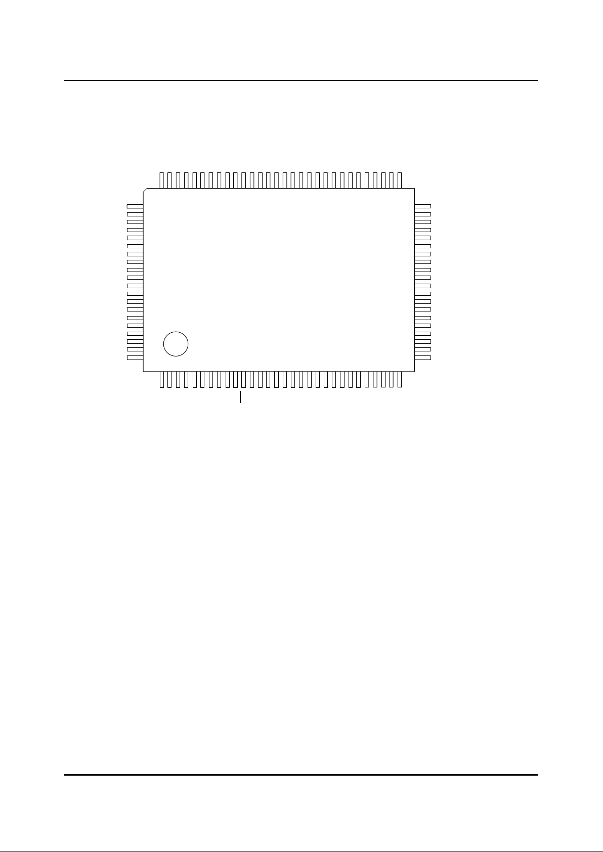
SANYO: SQFP100
S23/PC7
S22/PC6
S21/PC5
S20/PC4
S19/PC3
S18/PC2
S17/PC1
S16/PC0
S15/PB7
S14/PB6
S13/PB5
S12/PB4
S11/PB3
S10/PB2
S9/PB1
S8/PB0
S7/PA7
S6/PA6
S5/PA5
S4/PA4
S3/PA3
S2/PA2
S1PA1
S0/PA0
P73/INT3/T0IN
S47/PF7
V3/PL6
V2/PL5
V1/PL4
COM0/PL0
COM1/PL1
COM2/PL2
COM3/PL3
P30
P31
VSS3
VDD3
P32
P33
P34
P35
P00
P01
P02
P03
P04
P05
P06
P07
P10/SO0
P11/SI0/SB0
P12/SCK0
P13/SO1
P14/SI1/SB1
P15/SCK1
P16/T1PWM
L
P17/T1PWMH/BU
Z
RES
XT1/AN10
XT2/AN11
VSS1
CF1
CF2
VDD1
P80/AN0
P81/AN1
P82/AN2
P83/AN3
P84/AN4
P85/AN5
P86/AN6
P87/AN7/MICIN
P70/INT0/T0LCP/AN8
P71/INT1/T0HCP/AN9
P72/INT2/T0IN
S46/PF6
S45/PF5
S44/PF4
S43/PF3
S42/PF2
S41/PF1
S40/PF0
S39/PE7
S38/PE6
S37/PE5
S36/PE4
S35/PE3
S34/PE2
S33/PE1
S32/PE0
S31/PD7
S30/PD6
S29/PD5
S28/PD4
S27/PD3
S26/PD2
S25/PD1
S24/PD0
VSS2
VDD2
50
49
48
47
46
45
44
43
42
41
40
39
38
37
36
35
34
33
32
31
30
29
28
27
26
1 2 3 4 5 6 7 8 9
10
11
12
13
14
15
16
17
18
19
20
21
22
23
24
25
76
77
78
79
80
81
82
83
84
85
86
87
88
89
90
91
92
93
94
95
96
97
98
99
100
75747372717069686766656463626160595857565554535251
Page 7
LC8772C8B/B2B/96B/80B
No.6842-7/24
System Block Diagram
Interrupt Control
Stand-by C ontr ol
Clock
Generator
CF
RC
X’tal
IR PLA
ROM
PC
ACC
B Register
C Register
ALU
PSW
RAR
RAM
Stack Pointer
Watch Dog Timer
Bus Interface
Port 0
Port 1
Port 3
SIO0
SIO1
Timer 0
Timer 1
Base Timer
LCD Controller
INT0-3
Noise Re
j
ection Filter
Port 7
Port 8
ADC
Weak Signa Detector
Page 8
LC8772C8B/B2B/96B/80B
No.6842-8/24
Pin Assignment
Pin name I/O Function Option
VSS1
VSS2
VSS3
- • Power supply (-) No
VDD1
VDD2
VDD3
- • Power supply (+) No
PORT0
P00 to P07
I/O • 8bit input/output port
• Data direction programmable in nibble units
• Use of pull-up resistor can be specified in n ibble units
• Input for HOLD release
• Input for port 0 interrupt
Yes
PORT1
P10 to P17
I/O • 8bit input/output port
• Data direction programmable for each bit
• Use of pull-up resist or can be specified for each bit individually
• Other pin functions
P10 SIO0 data output
P11 SIO0 data input or bus input/output
P12 SIO0 clock input/output
P13 SIO1 data output
P14 SIO1 data input or bus input/output
P15 SIO1 clock input/output
P16: Timer 1 PWML output
P17: Timer 1 PWMH output/Buzzer output
Yes
PORT3
P30 to P35
I/O • 6bit Input/output port
• Data direction can b e specified for each bit
• Use of pull-up resist or can be specified for each bit individually
Yes
• 4bit Input/output port
• Data direction can b e specified for each bit
• Use of pull-up resist or can be specified for each bit individually
• Other func tions
P70: INT0 input/HOLD release input/Timer0L capture input/output for watchdog
timer
P71: INT1 input/HOLD release input/Timer0H capture input
P72: INT2 input/HOLD release input/timer 0 event input/Timer0L capture input
P73: INT3 input(noise rejection filter attached)/timer 0 event input/Timer0H capture
input
AD input port: AN8(P70), AN9(P71)
• Interrupt detection selection
Rising Falling Rising and
falling
H level L level
INT0
INT1
INT2
INT3
Yes
Yes
Yes
Yes
Yes
Yes
Yes
Yes
No
No
Yes
Yes
Yes
Yes
No
No
Yes
Yes
No
No
PORT7
P70 to P73
I/O
No
Page 9

LC8772C8B/B2B/96B/80B
No.6842-9/24
Pin name I/O Function description Option
PORT8
P80 to P87
I/O • 8bit Input/output port
• Input/output can be specified for each bit individ u ally
• Other func ti ons:
AD input port: AN0 to AN7
Small signal detector input port: MICIN(P87)
No
S0/PA0 to
S7/PA7
I/O • Segment output for L C D
• Can be used as general purpose input/output port (PA)
No
S8/PB0 to
S15/PB7
I/O • Segment output for L C D
• Can be used as general purpose input/output port (PB)
No
S16/PC0 to
S23/PC7
I/O • Segment output for L C D
• Can be used as general purpose input/output port (PC)
No
S24 /PD0to
S31/PD7
I/O • Segment output for LCD
• Can be used as general purpose input/output port (PD)
No
S32/PE0 to
S39/PE7
I/O • Segment output for L C D
• Can be used as general purpose input/output port (PE)
No
S40/PF0 to
S47/PF7
I/O • Segment output for L C D
• Can be used as general purpose input/output port (PF)
No
COM0/PL0 to
COM3/PL3
I/O • Com mon output for LCD
• Can be used as general purpose input port (PL)
No
V1/PL4 to
V3/PL6
I/O • LCD output bias power supply
• Can be used as general purpose input port (PL)
No
RES
I Reset terminal No
XT1 I • Input for 32.768kHz crystal oscillation
• Other func ti ons:
General purpose input port
AD input port: AN10
• When not in use, connect to VDD1
No
XT2 I/O • Output for 32.768kHz crystal oscillation
• Other func ti ons:
General purpose input port
AD input port: AN11
• When not in use, set to oscillation mode and leave open
No
CF1 I Input terminal for ceramic oscillator No
CF2 O Output terminal for ceramic oscillator No
Page 10

LC8772C8B/B2B/96B/80B
No.6842-10/24
Port Configuration
Port form and pull-up resistor options are shown in the following table.
Port status can be read even when port is set to output mode.
Terminal Option applies to: Options Output Form Pull-up resistor
1 CMOS Programmable
(Note 1)
P00 to P07 each bit
2 Nch-open drain None
1 CMOS Programmable P10 to P17 each bit
2 Nch-open drain Programmable
1 CMOS Programmable P30 to P35 each bit
2 Nch-open drain None
P70 – None Nch-open drain Programmable
P71 to P73 – None CMOS Programmable
P80 to P87 – None Nch-open drain None
S0/PA0 to
S47/PF7
– None CMOS Programmable
COM0/PL0 to
COM3/PL3
– None Input only None
V1/PL4 to
V3/PL6
– None Input only None
XT1 – None Input only None
XT2 – None Output for 32.768kHz crystal
oscillation
None
Note 1 Attachment of Port0 programmable pull-up resistors is controllable in nibble units (P00-03, P04-07).
* Note 1: Connect as follows to reduce noise on VDD.
VSS1, VSS2 and VSS3 must be connected together and grounded.
*Note 2 : The power supply for the internal memory is VDD1 but it uses the VDD3 as the power supply for ports. When the
VDD3 is not backed up, the port level does not become “H” even if the port latch is in the “H” level. Therefore,
when the VDD3 is not b acked up and the po rt latc h is “H” level , the por t level is unstabl e in the HOLD mode, and
the back up time becomes shorter because the through current runs from VDD to GND in the input buffer.
If VDD3 is not backed up, output “L” by the program or pull the port to “L” by the external circuit in the HOLD
mode so that the port level becomes “L” level and unnecessary current consumption is prevented.
LSI
VDD1
Back-up capacitors *2
VDD2
VDD3
VSS2 VSS1
Power
supply
VSS3
Page 11

LC8772C8B/B2B/96B/80B
No.6842-11/24
1. Absolute Maximum Ratings at Ta=25°C and VSS1=VSS2=VSS3=0V
Ratings
Parameter Symbol Pins Conditions
V
DD
[V]
min. typ. max.
unit
Supply voltage VDDMAX VDD1,VDD2,VDD3 VDD1=VDD2
=VDD3
-0.3 +7.0
Supply voltage
for LCD
VLCD V1/PL4, V2/PL5,
V3/PL6
VDD1=VDD2
=VDD3
-0.3 VDD
Input voltage VI Port L
XT1,XT2,CF1,
RES
-0.3 VDD+0.3
Input/Output
voltage
VI0(1) •Port0, 1, 3, 7, 8
•Port A, B, C, D, E, F
-0.3 VDD+0.3
V
IOPH(1) Port 0, 1, 3 •CMOS output
selected
•Current at each pin
-10
IOPH(2) Port 7 1,72,73 Current at each pin -3
Peak
output
current
IOPH(3) Port A, B, C, D, E, F Current at each pin -5
Σ
IOAH(1)
Port 0, 1, 32, 33, 34, 35 Total of all pins -40
Σ
IOAH(2)
Port 30, 31 Total of all pins -10
Σ
IOAH(3)
Port 7 Total of all pins -5
Σ
IOAH(4)
Port A, B, C Total of all pins -25
High
level
output
current
Total
output
current
Σ
IOAH(5)
Port D, E, F Total of all pins -25
IOPL(1) Port 0, 1, 32-35 Current at each pin 20
IOPL(2) Port 30, 31 Current at each pin 30
IOPL(3) Port 7,8 Current at each pin 5
Peak
output
current
IOPL(4) Port A, B,C, D, E, F Current at each pin 15
Σ
IOAL(1)
Port 0, 1, 32, 33, 34, 35 Total of all pins 60
Σ
IOAL(2)
Port 30, 31 Total of all pins 60
Low
level
output
current
Total
output
current
Σ
IOAL(3)
Port 7,8 Total of all pins 20
Σ
IOAL(4)
Port A,B,C Total of all pins 40
Σ
IOAL(5)
Port D, E, F Total of all pins 40
mA
QIP100E Maximum power
consumption
Pdmax
SQFP100
Ta = -30 to +70°C
mW
Operating
temperature
range
Topg -30 70
Storage
temperature
range
Tstg -55 125
°
C
Page 12

LC8772C8B/B2B/96B/80B
No.6842-12/24
2. Recommended Operating Range at Ta=-30°C to +70°C, VSS1=VSS2=VSS3=0V
Ratings
Parameter Symbol Pins Conditions
VDD
[V]
min. typ. max.
unit
VDD(1)
0.294µs ≤ t
CYC
≤
200µs
4.5 6.0
Operating
supply voltage
range
VDD(2)
VDD1=VDD2=VDD3
0.735µs ≤ t
CYC
≤
200µs
2.5 6.0
Supply voltage
range in Hold
mode
VHD VDD1 Keep RAM and
register data in
HOLD mode.
2.0 6.0
VIH(1) •Port 0, 3, 8
•Port A,B,C,D,E,F,L
Output disable 2.5 to 6.0 0.3VDD
+0.7
VDD
VIH(2) •Port 1
•Port 71,72, 73
•P70 port input/interrupt
Output disable 2.5 to 6.0 0.3VDD
+0.7
VDD
VIH(3) P87 small signal input Output disable 2.5 to 6.0 0.75VDD VDD
VIH(4) Port 70
Watchdog timer
Output disable 2.5 to 6.0 0.9VDD VDD
Input high
voltage
VIH(5)
XT1, XT2, CF1,
RES
2.5 to 6.0 0.75VDD VDD
VIL(1) •Port 0, 3, 8
•Port A,B,C,D,E,F,L
Output disable 2.5 to 6.0 VSS 0.15VDD
+0.4
VIL(2) •Port 1
•Port 71,72, 73
•P70 port input/interrupt
Output disable 2.5 to 6.0 VSS 0.1VDD
+0.4
VIL(3) Port 87 small signal input Output disable 2.5 to 6.0 VSS 0.25VDD
VIL(4) Port 70
Watchdog timer
Output disable 2.5 to 6.0 VSS 0.8VDD
-1.0
Input low
voltage
VIL(5)
XT1,XT2,CF1,
RES
2.5 to 6.0 VSS 0.25VDD
V
4.5 to 6.0 0.294 200 Operation
cycle time
t
CYC
2.5 to 6.0 0.735 200
µ
s
4.5 to 6.0 0.1 10 •CF2 open
•system clock
divider :1/1
•external clock
DUTY = 50±5%
2.5 to 6.0 0.1 4
4.5 to 6.0 0.2 20
External system
clock
frequency
FEXCF(1) CF1
•CF2 open
•system clock
divider :1/2
2.5 to 6.0 0.2 8
MHz
Continued/
Page 13

LC8772C8B/B2B/96B/80B
No.6842-13/24
Ratings
Parameter Symbol Pins Conditions
VDD[V] min. typ. max.
unit
FmCF(1) CF1, CF2 10MHz ceramic resonator
oscillation
Refer to f igure 1
4.5 to 6.0 10
FmCF(2) CF1, CF2 4MHz ceramic resonat or
oscillation
Refer to f igure 1
2.5 to 6.0 4
FmRC RC oscillation 2.5 to 6.0 0.3 1.0 2.0
MHz
Oscillation
frequency
range
(Note 1)
FsX’tal XT1, XT2 32.768kHz crystal resonator
oscillation
Refer to f igure 2
2.5 to 6.0 32.768 kHz
(Note 1) The port value of oscillation circuit is shown in table 1 and table 2.
Page 14

LC8772C8B/B2B/96B/80B
No.6842-14/24
3. Electrical Characteristics at Ta=-30°C to +70°C, VSS1=VSS2=VSS3=0V
Ratings
Parameter Symbol Pins Conditions
VDD[V] min. typ. max.
unit
IIH(1) •Port 0,1,3,7,8
•Port A,B,C,D,E,F,L
•Output disabled
•Pull-up resister OFF.
•VIN=VDD
(including OFF st ate leak
current of the output Tr.)
2.5 to 6.0 1
IIH(2)
RES
VIN=VDD 2.5 to 6.0 1
IIH(3) XT1,XT2 When configured as an input
port
VIN=VDD
2.5 to 6.0 1
IIH(4) CF1 VIN=VDD 2.5 to 6.0 15
High level
input
current
IIH(5) P87/AN7/MICIN
small signal input
VIN=V
BIS
+0.5V
(V
BIS
: Bias voltage)
2.5 to 6.0 4.2 8.5 15
IIL(1) •Port 0,1,3,7,8
•Port A,B,C,D,E,F,L
•Output disabled
•Pull-up resister OFF.
•VIN=VSS
(including OFF state leak
current of the output Tr.)
2.5 to 6.0 -1
IIL(2)
RES
VIN=VSS 2.5 to 6.0 -1
IIL(3) XT1,XT2 When configured as an input
port
VIN=VSS
2.5 to 6.0 -1
IIL(4) CF1 VIN=VSS 2.5 to 6.0 -15
Low level
input
current
IIL(5) P87/AN7/MICIN
small signal input
VIN=V
BIS
-0.5V
(V
BIS
: Bias voltage)
2.5 to 6.0 -15 -8.5 -4.2
µ
A
VOH(1) IOH=-1.0mA 4.5 to 6.0 VDD-1
VOH(2)
Port 0,1,3: CMOS
output option
IOH=-0.1mA 2.5 to 6.0 VDD-0.5
VOH(3) Port 7 IOH=-0.4mA 2.5 to 6.0 VDD-1
VOH(4) IOH=-1.0mA 4.5 to 6.0 VDD-1
High level
output
voltage
VOH(5)
Port A,B,C,D,E,F
IOH=-0.1mA 2.5 to 6.0 VDD-0.5
VOL(1) IOL=10mA 4.5 to 6.0 1.5
VOL(2)
Port 0,1,3
IOL=1.6mA 2.5 to 6.0 0.4
VOL(3) Port 30,31 IOL=30mA 4.5 to 6.0 1.5
VOL(4) IOL=1mA 4.5 to 6.0 0.4
VOL(5)
Port 7,8
IOL=0.5mA 2.5 to 6.0 0.4
VOL(6) IOL=8mA 4.5 to 6.0 1.5
Low level
output
voltage
VOL(7)
Port A,B,C,D,E,F
IOL=1.4mA 2.5 to 6.0 0.4
VODLS S0–S47 I0=0mA
VLCD, 2/3VLC D,
1/3VLCD level output
Refer to figure 8
2.5 to 6.0 0 ±0.2
LCD output
voltage
regulation
VODLC COM0–COM3 I0=0mA
VLCD, 2/3VLC D, 1/2VLCD
1/3VLCD level output
Refer to figure 8
2.5 to 6.0 0 ±0.2
V
RLCD(1) Resistance per one
bias resistor
Refer to figure 8 2.5 to 6.0 60 LCD bias
resistor
RLCD(2) •Resistance per one
bias resistor
•1/2 R mode
Refer to figure 8 2.5 to 6.0 30
kΩ
Continued/
Page 15

LC8772C8B/B2B/96B/80B
No.6842-15/24
Ratings
Parameter Symbol Pins Conditions
VDD[V] min. typ. max.
unit
4.5 to 6.0 15 40 70 Resistance of
pull-up
MOS Tr.
Rpu •Port 0,1,3,7
•Port A,B,C,D,E,F
VOH=0.9VDD
2.5 to 4.5 25 70 150
kΩ
VHIS(1) •Port 1,7
•
RES
2.5 to 6.0
0.1VDD
Hysterisis
voltage
VHIS(2) Port 87 small signal
input
2.5 to 6.0
0.1VDD
V
Pin
capacitance
CP All pins •All other terminals connected
to VSS.
•f=1MHz
•
T
a
=25°C
2.5 to 6.0 10 pF
Input
sensitivity
Vsen Port 87 small signal
input
2.5 to 6.0 0.12VDD Vpp
Page 16

LC8772C8B/B2B/96B/80B
No.6842-16/24
4. Serial Input/Output Characteristics at Ta=-30°C to +70°C, VSS1=VSS2=VSS3=0V
Ratings
Parameter Symbol Pins Conditions
VDD[V] min. typ. max.
unit
Cycle time tSCK(1) 4/3
tSCKL(1)
2/3 Low level
pulse width
tSCKLA(1)
2/3
tSCKH(1)
2/3 High level
pulse width
tSCKHA(1)
SCK0(P12) Refer to figure 6 2.0 to 6.0
3
Cycle time tSCK(2)
2
Low level
pulse width
tSCKL(2)
1
Input clock
High level
pulse width
tSCKH(2)
SCK1(P15) Refer to figure 6 2.5 to 6.0
1
Cycle time tSCK(3)
4/3
t
CYC
tSCKL(3)
1/2 Low level
pulse width
tSCKLA(2)
3/4
tSCKH(3)
1/2 High level
pulse width
tSCKHA(2)
SCK0(P12) •CMOS output
•Refer to figure 6
2.5 to 6.0
2
tSCK
Cycle time tSCK(4)
2 tCYC
Low level
pulse width
tSCKL(4)
1/2
Serial clock
Output clock
High level
pulse width
tSCKH(4)
SCK1(P15) •CMOS output
•Refer to figure 6
2.5 to 6.0
1/2
tSCK
4.5 to 6.0 0.03
Data set-up time
t
sDI
2.5 to 6.0 0.1
4.5 to 6.0 0.03
Serial input
Data hold time t
hDI
SI0(P10),
SI1(P13),
SB0(P11),
SB1(P14)
•Measured with respect
to SI0CLK leading
edge.
•Refer to figure 6
2.5 to 6.0 0.1
4.5 to 6.0 1/3
tCYC
+0.05
Serial output
Output delay
time
tdDO SO0(P12),
SO1(P15),
SB0(011),
SB1(P14)
•When Port is open
drain:
Time delay form
SIOCLK trailing edge
to the SO data change
•Refer to figure 6
2.5 to 6.0 1/3
tCYC
+0.25
µ
s
Page 17

LC8772C8B/B2B/96B/80B
No.6842-17/24
5. Pulse Input Conditions at Ta=-30°C to +70°C, VSS1=VSS2=VSS3=0V
Ratings
Parameter Symbol Pins Conditions
VDD[V] min. typ. max.
unit
tPIH(1)
tPIL(1)
INT0(P70),
INT1(P71),
INT2(P72)
•Condition that interrupt is
accepted
•Condition that event input
to timer 0 is accepted
2.5 to 6.0 1
tPIH(2)
tPIL(2)
INT3(P73)
(Noise rejection ratio
is 1/1.)
•Condition that interrupt is
accepted
•Condition that event input
to timer 0 is accepted
2.5 to 6.0 2
tPIH(3)
tPIL(3)
INT3(P73)
(Noise rejection ratio
is 1/32.)
•Condition that interrupt is
accepted
•Condition that event input
to timer 0 is accepted
2.5 to 6.0 64
tPIH(4)
tPIL(4)
INT3(P73)
(Noise rejection ratio
is 1/128.)
•Condition that interrupt is
accepted
•Condition that event input
to timer 0 is accepted
2.5 to 6.0 256
tPIL(5)
tPIL(5)
MICIN(P87) •Condition that signal is
accepted to small signal
detection counter.
2.5 to 6.0 1
t
CYC
High/low level
pulse width
tPIL(6)
RES
•Condition that reset is
accepted
2.5 to 6.0 200
µ
s
6. AD Converter Characteristics at Ta=-30°C to + 70°C, VSS1=VSS2=VSS3=0V
Ratings
Parameter Symbol Pins Conditions
VDD[V] min. typ. max.
unit
Resolution N 3.0 to 6.0 8 bit
Absolute precision ET (Note2) 3.0 to 6.0
±
1.5
LSB
4.0 to 6.0 15.62
(tCYC=
0.488µs)
97.92
(tCYC=
3.06µs)
AD conversion time
= 32 × tCYC
(ADCR2=0)
(Note 3)
3.0 to 6.0 23.52
(tCYC=
0.735µs)
97.92
(tCYC=
3.06µs)
4.5 to 6.0 18.82
(tCYC=
0.294µs)
97.92
(tCYC=
1.53µs)
Conversion time TCAD
AD conversion time
= 64 × tCYC
(ADCR2=1)
(Note 3)
3.0 to 6.0 47.04
(tCYC=
0.735µs)
97.92
(tCYC=
1.53µs)
µ
s
Analog input
voltage range
VAIN 3.0 to 6.0 VSS VDD V
IAINH VAIN=VDD 3.0 to 6.0 1 Analog port input
current
IAINL
AN0(P80)
–AN7(P87)
AN8(P70)
AN9(P71)
AN10(XT1)
AN11(XT2)
VAIN=VSS 3.0 to 6.0 -1
µ
A
(Note 2) Abso lute precision does not include quantizing error (±1/2 LSB).
(Note 3) Conversion time means time from executing AD conversion instruction to loading complete digital value to register.
Page 18

LC8772C8B/B2B/96B/80B
No.6842-18/24
7. Current Consumption Characteristics at Ta=-30°C to +70°C, VSS1=VSS2=VSS3=0V
Ratings
Parameter Symbol Pins Conditions
VDD[V] min. typ. max
unit
IDDOP(1) •FmCF=10MHz
Ceramic resonator
oscillation
•FsX’tal=32.768kHz
crystal oscillation
•System clock: CF
10MHz oscillation
•Internal RC oscillation
stopped.
•Divider : 1/1
4.5 to 6.0
IDDOP(2) •CF1=20MHz external
clock
•FsX’tal=32.768kHz
crystal oscillation
•System clock: CF1
oscillation
•Internal RC oscillation
stopped.
•Divider :1/ 2
4.5 to 6.0
IDDOP(3) 4.5 to 6.0
IDDOP(4)
•FmCF=4M Hz Ceramic
resonator oscillation
•FsX’tal=32.768kHz
crystal oscillation
•System clock: CF
4MHz oscillation
•Internal RC oscillation
stopped.
•Divider :1/ 1
2.5 to 4.5
IDDOP(5) 4.5 to 6.0
IDDOP(6)
•FmCF=0Hz (No
oscillation)
•FsX’tal=32.768kHz
crystal oscillation
•System clock: RC
oscillation
•Divider :1/ 2
2.5 to 4.5
mA
IDDOP(7) 4.5 to 6.0
Current consumption
during normal
operation
(Note 4)
IDDOP(8)
VDD1=
VDD2=
VDD3
•FmCF=0Hz (No
oscillation)
•FsX’tal=32.768kHz
crystal oscillation
•System clock:
32.768kHz
•Internal RC oscillation
stopped.
•Divider :1/ 2
2.5 to 4.5
µ
A
Continued/
Page 19

LC8772C8B/B2B/96B/80B
No.6842-19/24
Ratings
Parameter Symbol Pins Conditions
VDD[V] min. typ. max.
unit
IDDHALT(1) HALT mode
•FmCF=10MHz Ceramic
resonator oscillation
•FsX’tal=32.768kHz
crystal oscillation
•System clock :
CF 10MHz oscillation
•Internal RC oscillation
stopped.
•Divider: 1/1
4.5 to 6.0
IDDHALT(2) HALT mode
•CF1=20MHz for extern al
clock
•FsX’tal=32.768kHz
crystal oscillation
•System clock :
CF1 oscillation
•Internal RC oscillation
stopped.
•Divider :1/2
4.5 to 6.0
IDDHALT(3) 4.5 to 6.0
IDDHALT(4)
V
DD1=
V
DD2=
V
DD3
HALT mode
•FmCF=4M Hz Ceramic
resonator oscillation
•FsX’tal=32.768kHz
crystal oscillation
•System clock :
CF 4MHz oscillation
•Internal RC oscillation
stopped.
•Divider: 1/1
2.5 to 4.5
mA
IDDHALT(5) 4.5 to 6.0
IDDHALT(6)
HALT mode
•FmCF=0Hz
(Oscillation stop)
•FsX’tal=32.768kHz
crystal oscillation
•System clock :
RC oscillation
•Divider: 1/2
2.5 to 4.5
IDDHALT(7) 4.5 to 6.0
Current
consumption
during
HALT mode
(Note 4)
IDDHALT(8)
HALT mode
•FmCF=0Hz
(Oscillation stop)
•FsX’tal=32.768kHz
crystal oscillation
•System clock : 32.768kHz
•Internal RC oscillation
stopped.
•Divider: 1/2
2.5 to 4.5
µ
A
Continued/
Page 20

LC8772C8B/B2B/96B/80B
No.6842-20/24
Ratings
Parameter Symbol Pins Conditions
VDD[V] min. typ. max.
unit
IDDHOLD(1) 4.5 to 6.0 Current consumption
during HOLD mode
IDDHOLD(2)
VDD1 HOLD mode
•CF1=VDD or open
(when using external
clock)
2.5 to 4.5
IDDHOLD(3) 4.5 to 6.0 Current consumption
during Date/time
clock HOLD mode
IDDHOLD(4)
VDD1 Date/time clock HOLD
mode
•CF1=VDD or open
(when using external
clock)
•FmX’tal=32.768kHz
crystal oscillation
2.5 to 4.5
µ
A
(Note 4) The currents through the output transistors and the pull-up MOS transistors are ignored.
Page 21

LC8772C8B/B2B/96B/80B
No.6842-21/24
Main system clock osci llation circuit characteristics
The characteristics in the table bellow is based on the following conditions:
1. Use the standard evaluation board SANYO has provided.
2. Use the peripheral parts with indicated value externally.
3. The peripheral parts value is a recommended value of oscillator manufacturer
Table 1. Main system clock oscillation circuit charac teris tics using ceramic resonator
Circuit parameters
Oscillation
stabilizing time
Frequency Manufacturer Oscillator
C1 C2 Rd1
Operating
supply voltage
range
typ max
Notes
10MHz
4MHz
The oscillation stabilizing time is a period until the oscillation becomes stable after VDD becomes higher than
minimum operating voltage. (Refer to Figure4)
Subsystem clock oscillation circuit characteristics
The characteristics in the table bellow is based on the following conditions:
1. Use the sta nda rd evaluation board SANYO has pro vided.
2. Use the peripheral parts with indicated value externally.
3. The peripheral parts value is a recommended value of oscillator manufacturer
Table 2. Subsystem clock oscillation circuit characteris tics using crystal oscil lator
Circuit parameters
Oscillation
stabilizing time
Frequency Manufacturer Oscillator
C3 C4 Rf Rd2
Operating
supply voltage
range
typ max
Notes
32.768kHz
The oscillation stabilizing time is a period until the oscillation becomes stable after executing the instruction which starts the
sub-clock oscillation or after releasing the HOLD mode. (Refer to Figure4)
(Notes) • Since the circuit pattern affects the oscillation frequency, place the oscillation-related parts as close to
the oscillation pins as possible with the shortest possible pattern length.
Figure 1 Ceramic oscillation circuit Figure 2 Crystal oscillation circuit
C3
Rd2
C4
X’tal
XT2 XT1
Rf
C1
C2
CF
CF2 CF1
Rd1
Page 22

LC8772C8B/B2B/96B/80B
No.6842-22/24
Figure 3 AC timing measurement po int
Reset time and oscillation stable time
HOLD release signal and oscillation stable time
Figure 4 Oscillation stabilizing time
0.5VDD
Power Supply
RES
Internal RC
Resonator oscillation
CF1
,
CF2
XT1
,
XT2
Operation mode
Reset time
tmsCF
tmsXtal
Unfixed
Rese t Instruction exe cution mode
VDD
VDD limit
0V
Internal RC
Resonator oscillation
CF1,CF2
XT1,XT2
Operation mode
HOLD release signal
Without HOLD
Release signal
HOLD release signal VALID
tmsCF
tmsXtal
HOLD HALT
Page 23

LC8772C8B/B2B/96B/80B
No.6842-23/24
Figure 5 Reset circuit
Figure 6 Serial input / output wave form
(Note)
Select CRES and RRES value to assure that at least 200µs
reset time is gene rated aft er the VDD b ecomes highe r than
the minimum operating voltage.
C
RES
VDD
R
RES
RES
SIOCLK
DATAIN
DATAOUT
DI0 DI1 DI2 DI3 DI4 DI5 DI6 DI7 DI8
DO0 DO1 DO2 DO3 DO4 DO5 DO6 DO7 DO8
Data RAM
transmission period
(only SIO0)
SIOCLK
DATAIN
DATAOUT
tSCK
tSCKL tSCKH
tsDI thDI
tdDO
SIOCLK
DATAIN
DATAOUT
tdDO
tsDI thDI
tSCKLA tSCKHA
Data RAM
transmission period
(only SIO0)
Page 24

LC8772C8B/B2B/96B/80B
No.6842-24/24
Figure 7 Pulse input timing
Figure 8 LCD bias resistor
PS
tPIL tPIH
VLCD
SW : ON
(
VLCD=VDD)
2/3VLCD
1/2VLCD
1/3VLCD
SW : ON/OFF(programmable)
4R
2R
R
R
2R
VDD
GND
 Loading...