

Page 1
Ordering number : ENN*6805
LC86E5420
LC86E5420
8-Bit Single Chip Microcontroller
Preliminary
Overview
The LC86E5420 is a CMOS 8-bit single chip microcontroller with UVEPROM of the LC865500 / LC865400
series.
This microcontroller has the function and the pin discription of the LC865500 / LC865400 series mask ROM
version, and the 20K-byte EPROM. The program data is rewritable. It is suitable to develop the program.
Features
(1) Option switching by EPROM data
The option function of the LC865400 series can be specified by the EPROM data.
The LC86E5420 can be checked the functions of the trial pieces using the mass production board.
(2) Internal EPROM capacity : 20736 bytes
(3) Internal RAM capacity : 512 bytes
CMOS IC
Mask ROM version PROM capacity RAM capacity
LC865520 20480 bytes 512 bytes
LC865516 16384 bytes 512 bytes
LC865512 12288 bytes 512 bytes
LC865508 8192 bytes 512 bytes
LC865504 4096 bytes 512 bytes
LC865412 12288 bytes 224 bytes
LC865408 8192 bytes 224 bytes
LC865404 4096 bytes 224 bytes
(4) Operating supply voltage : 4.5V to 6.0V
(5) Instruction cycle time : 1.0µs to 366µs
(6) Operating temperature : +10°C to +40°C
(7) The pin compatible with the LC865400 series mask ROM devices
(8) Applicable mask ROM version : LC865520 / LC865516 / LC865512 / LC865508 / LC865504
LC865412 / LC865408 / LC865404
(9) Factory shipment : DIC42S (with window)
QIC48E (with window)
Ver. 2.00
31395
Any and all SANYO products described or contained herein do not have specifications that can handle
applications that require extremely high levels of reliability, such as life-support systems, aircraft's
control systems, or other applications whose failure can be reasonably expected to result in serious
physical and/or material damage. Consult with your SANYO representative nearest you before using
any SANYO products described or contained herein in such applications.
SANYO assumes no responsibility for equipment failures that result from using products at values that
exceed, even momentarily, rated values (such as maximum ratings, operating condition ranges, or other
parameters) listed in products specifications of any and all SANYO products described or contained
herein.
SANYO Electric Co.,Ltd. Semiconductor Company
TOKYO OFFICE Tokyo Bldg., 1-10, 1 Chome, Ueno, Taito-ku, TOKYO, 110-8534 JAPAN
D2000 RM (IM) FS
No.6805-1/21
Page 2
LC86E5420
Notice for use
The LC86E5420 is provided for the first release and small shipping of the LC865500 / LC865400 series.
At using, take notice of the followings.
(1) A point of difference the LC86E5420 and the LC865500 / LC865400 series
Item LC86E5420
Operation after reset The option is specified by degreess until 3ms The program is executed from 00H of
releasing after going to a 'H' level to the reset terminal. the program counter immediately after
The program is executed from 00H of the going to a 'H' level to the reset terminal.
program counter.
Operating supply 4.5V to 6.0V 2.5V to 6.0V
voltage range (VDD)
Operating temperature +10 to +40°C -- 30 to +70°C
range (Topg)
Power dissipation Refer to 'electrical characteristics' on the semiconductor news.
The LC86P5420 functions same as the followings while resetting ; LC865520 / 16 / 12 / 08 / 04, LC865412 / 08 /
04.
The LC86E5420 uses 256 bytes that is addressed on 7F00H to 7FFFH in the program memory as the option
configulation data area.
• A kind of the option corresopnding of the LC86E5420
A kind of option Pins, Circuits Contents of the option
Input / output form of Port 0 1. N-channel open drain output
input / output ports 2. CMOS output *1
1. Pull-up MOS Tr. provided
2. Pull-up MOS Tr. not provided *2
Port 1 1. Input : Programmable pull-up MOS Tr.
Output : N-channel open drain
2. Input : Programmable pull-up MOS Tr.
*1 Output : CMOS
Port 3 1. Input : No Programmable pull-up
Output : N-channel open drain
2. Input : Programmable pull-up MOS Tr.
*1 Output : CMOS
*1) Specified in bit
*2) Specified in nibble unit. Pull-up MOS Tr. is not provided in N-channel open drain output port.
LC865520 / 16 / 12 / 08 / 04 / LC865412 / 08 / 04
MOS Tr.
(2) Option
The option data is created by the option specified program "SU86K.EXE". The created option data is
linked to the program area by the linkage loader "L86K.EXE".
No.6805-2/21
Page 3
LC86E5420
(3) ROM space
The LC86E5420 and LC865500 / LC865400 series use 256 bytes that is addressed on 7F00H to 7FFFH in the
program memory as the option specified data area. These program memory capacity are 20480 bytes that is
addressed on 0000H to 4FFFH.
7FFFH
7F00H
6FFFH
5FFFH
4EFFH
3FFFH
2FFFH
1FFFH
0FFFH
0000H
Option Data area
256 bytes
Program Area
20K bytes
LC865520
Option
Data area
Program Area
16K bytes
LC865516
Option
Data area
Program Area
12K bytes
LC865512
LC865412
Option
Data area
Program Area
8K bytes
LC865508
LC865408
Option
Data area
Program Area
4K bytes
LC865504
LC865404
How to use
(1) Create a programming data for LC86E5420
Programming data for EPROM of the LC86E5420 is required.
Debugged evaluation file (EVA file) must be converted to an INTEL-HEX formatted file (HEX file) with file
converter program, EVA2HEX.EXE. The HEX file is used as the programming data for the LC86E5420.
(2) How to program for the EPROM
The LC86E5420 can be programmed by the EPROM programmer with attachment ; W86EP5420D,
W86EP5420Q.
• Recommended EPROM programmer
Productor EPROM programmer
Advantest R4945, R4944, R4943
Andou AF-9704
AVAL PKW-1100, PKW-3000
Minato electronics MODEL1890A
• "27512 (Vpp=12.5V) Intel high speed programming" mode available. The address must be set to
"0000H to 7FFH" and a jumper (DASEC) must be set to 'OFF' at programming.
No.6805-3/21
Page 4
LC86E5420
(3) How to use the data security function
"Data security" is the disabled function to read the data of the EPROM.
The following is the process in order to execute data security.
1. Set 'ON' the jumper of attachment.
2. Program again. Then the EPROM programmer displays the error. The error means normally activity of the
data security. It is not a trouble of the EPROM programmer or the LSI.
Notes
• Data security is not executed when the data of all address have 'FFH' at the sequence 2 above.
• The programming by sequential operation "BLANK→PROGRAM→VERIFY" cannot be executed data
security at the sequence 2 above.
• Set 'OFF' to the jumper after executing the data security.
(4) How to eliminate
The programming data can be erased by using the EPROM eraser.
(5) Shielding
The UVEPROM (ultraviolet erasable and programmable ROM) is in it. Put the seal on the window in use.
Data security Data security
Not data security Not data security
W86EP5420D W86EP5420Q
No.6805-4/21
Page 5
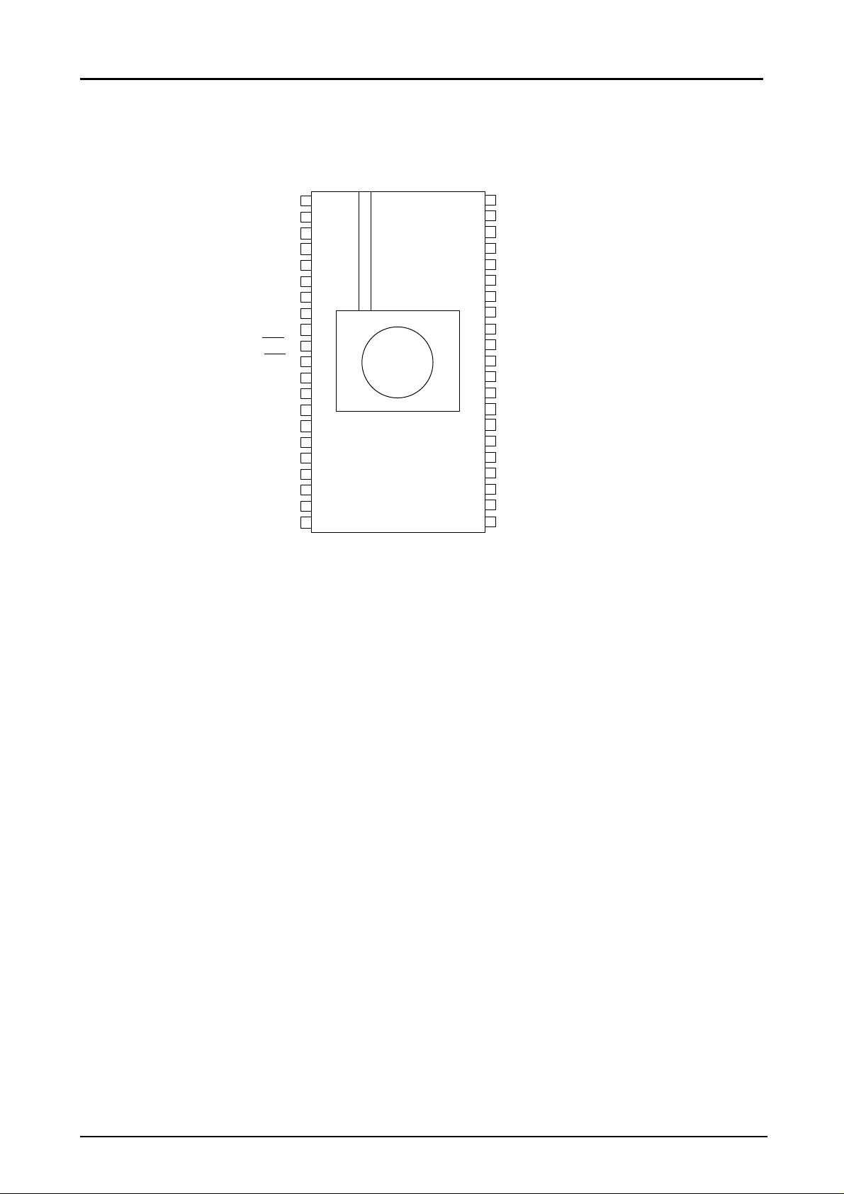
Pin Assignment
• DIC42S
LC86E5420
P00
P01
P02
P03
P04
P05
P06
P07
P70 / INT0
RES
XT1 / P74
XT2 / P75
V
SS
CF1
CF2
V
DD
P80 / AN0
P81 / AN1
P82 / AN2
P83 / AN3
P84 / AN4
1
2
3
4
5
6
7
8
9
10
11
12
13
14
15
16
17
18
19
20
21 22
42
41
40
39
38
37
36
35
34
33
32
31
30
29
28
27
26
25
24
23
P17 / PWM0
P16 / BUZ
P15 / SCK1
P14 / S11 / SB1
P13 / SO1
P12 / SCK0
P11 / SI0 / SB0
P10 / SO0
P36
P35
P34
P33
P32
P31
P30
P73 / INT3 / T0IN
P72 / INT2 / T0IN
P71 / INT1
P87 / AN7
P86 / AN6
P85 / AN5
ILC00015
No.6805-5/21
Page 6
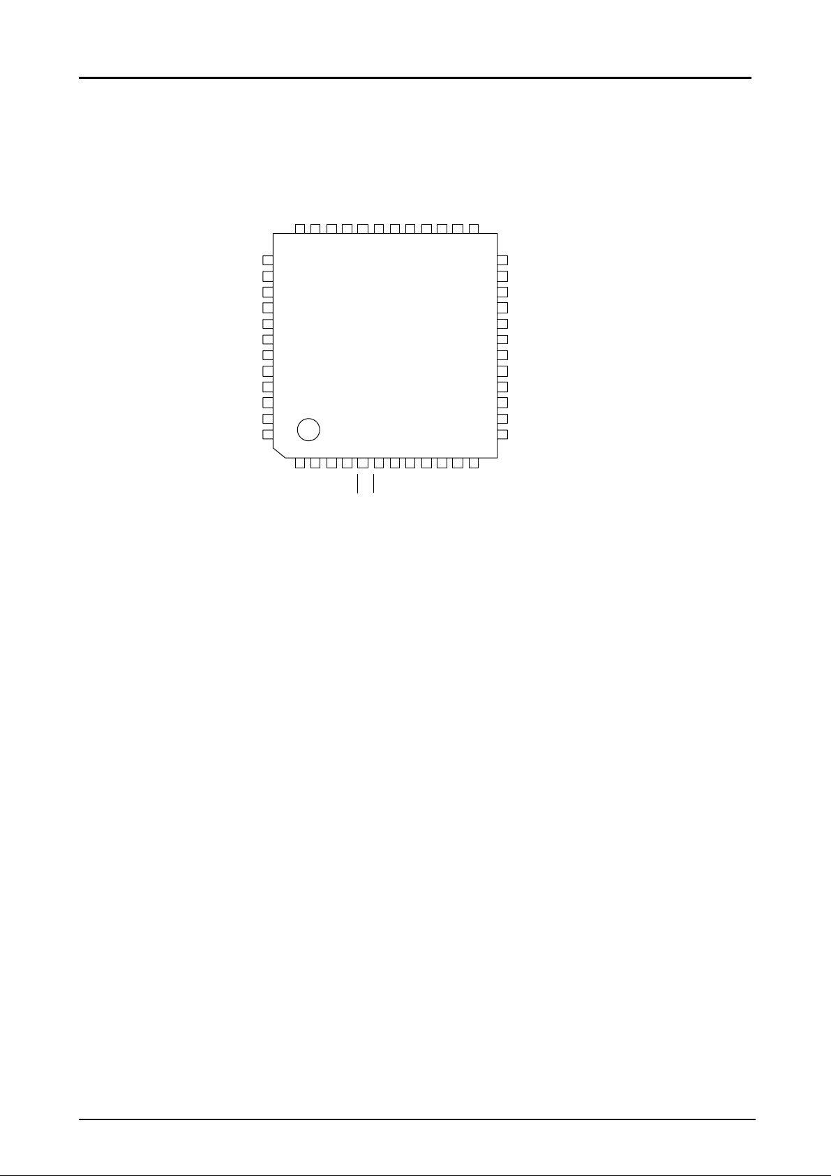
• QIC48E
P12 / SCK0
P11 / SI0 / SB0
P10 / SO0
LC86E5420
P35
P33NCP32
P34
P36
P31
P30
P73 / INT3 / T0IN
P13 / SO1
P14 / SI1 / SB1
P15 / SCK1
P16 / BUZ
P17 / PWM0
NC
P00
P01
P02
P03
P04
NC
363534
37
38
39
40
41
42
43
44
45
46
47
48
123456789
P05
P06
33
P07
P70 / INT0
32
RES
31302928272625
101112
SS
NC
XT1 / P74
CF1
V
XT2 / P75
CF2
24
23
22
21
20
19
18
17
16
15
14
13
V
DD
NC
P72 / INT2 / T0IN
P7I / INT1
P87 / AN7
P86 / AN6
P85 / AN5
NC
P84 / AN4
P83 / AN3
P82 / AN2
P81 / AN1
P80 / AN0
ILC00010
No.6805-6/21
Page 7
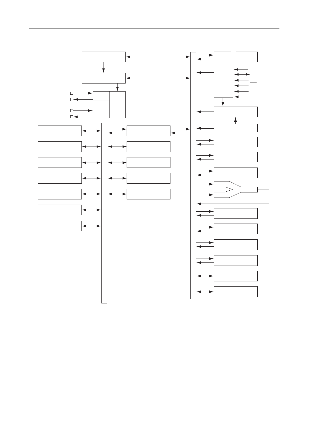
System Block Diagram
LC86E5420
Base Timer
SIO0
SIO1
Timer0
Timer1
Interrupt Control
Stand-by Control
CF
RC
X’tal
Clock
Generator
Bus Interface
Port 1
Port 3
Port 7
Port 8
IR PLA
EPROM
Control
EPROM(32KB)
PC
ACC
B Register
C Register
A14--A0
D7--D0
TA
CE
OE
DASEC
ALU
ADC
INT0 to 3
Noise Filter
PSW
RAR
RAM
Stack Pointer
Port 0
W atchdog Timer
ILC00035
No.6805-7/21
Page 8

LC86E5420
Pin Description
Pin name I / O Function description Option PROM mode
V
SS
V
DD
PORT0 I / O •8-bit input / output port •Pull-up resistor :
P00 to P07 Input / output in nibble units Provided / Not provided
PORT1 I / O •8-bit input / output port •Output form : Data line
P10 to P17 Input / output can be specified in bit unit.
PORT3 I / O •7-bit input / output port •Pull-up resistor :
P30 to P36 Input / output in bit unit. Provided / Not provided
PORT7 •4-bit input / output port
P70 to P73 I / O P70 : INT0 input / HOLD release input / EPROM control signals
P74, P75 I P71 : INT1 input / HOLD release input •OE (*2)
Power pin (-- )
Power pin (+)
•Input for port 0 interrupt (specify every 4-bit)
•Input for HOLD release •Output form :
•15V withstand at N-channel open drain
output (specify in bit)
•Other pin functions (specify in bit)
P10 SIO0 data output
P11 SIO0 data input / bus input / output
P12 SIO0 clock input / output
P13 SIO1 data output
P14 SIO1 data input / bus input / output
P15 SIO1 clock input / output
P16 Buzzer output
P17 Timer1 (PWM0) output
•15V withstand at N-channel open drain •Output form :
output
Input / output in bit unit.
•2-bit input port
•Other pin functions.
N-channel
P72 : INT2 input / timer 0 event input •CE (*3)
P73 : INT3 input with noise filter / timer 0
event input
P74 : Input pin XT1 for 32.768kHz crystal
oscillation
P75 : Output pin XT2 for 32.768kHz crystal
oscillation
•Interrupt received form, vector address
Rising Falling & Vector
INT0 enable enable disable enable enable 03H
INT1 enable enable disable enable enable 0BH
INT2 enable enable enable disable disable 13H
INT3 enable enable enable disable disable 1BH
Tr. output for watchdog timer
Rising
Falling
High Low
level level
CMOS / N-channel open drain
CMOS / N-channel open drain.
CMOS / N-channel open drain
D0 to D7
•DASEC (*1)
No.6805-8/21
Page 9

LC86E5420
Pin name I / O Function description Option PROM mode
PORT8
P80 to P83 I •4-bit input port TA (*4)
P84 to P87 I / O •4-bit input / output port
Input / output can be specified in bit unit
•Other function
AD input port (AN7 to AN0)
RES I Reset pin.
XT1 / P74 I •
XT1 / P75 O •
CF1 I
CF2 O
All of port options except the pull-down resistor option of Port 0 can be specified in a bit unit.
Input pin for the 32.768kHz cyrstal oscillation
•Other function
XT1 : Input port P74
•In case of non use, connect to V
Output pin for the 32.768kHz cyrstal oscillation
•Other function
XT2 : Input port P75
•
In case of non use, connect to VDD at using
as port or unconnect at using as oscillation.
Input pin for the ceramic resonator oscillation.
Output pin for the ceramic resonator oscillation.
DD
*1 Memory select input for data security
*2 Output enable input
*3 Chip enable input
*4 TA → EPROM control signal input
No.6805-9/21
Page 10

LC86E5420
1. Absolute Maximum Ratings at V
Parameter Symbol Pins Conditions
Supply voltage VDD MAX V
Input voltage VI(1) •Ports 74, 75 -- 0.3
Input/output VIO(1) •Port 1 -- 0.3
voltage •
VIO(2) Ports 0, 3 at N-ch -- 0.3 15
High Peak IOPH •Ports 0, 1, 3 CMOS output -- 10 mA
Level output •Ports 71, 72, 73 At each pins
output current •
current Total ∑IOAH(1) Ports 0,1 The total all -- 30
output pins
current ∑IOAH(2) Port 3 The total all -- 15
∑IOAH(3) •Ports 71, 72, 73 The total all -- 10
Low Peak IOPL(1) Ports 0, 1, 3 At each pins 20
Level output IOPL(2) •
output current •
current Total ∑IOAL(1) Ports 0, 1, 70 The total all 60
output pins
current ∑IOAL(2) Port 3 The total all 40
∑IOAL(3) •Ports 71, 72, 73 The total all 20
Power Pdmax (1) DIC42S
dissipation Pdmax (2) QIC48E
(max.)
Operating Topr +10 +40 °C
temperature
range
Storage Tstg -- 65 150
temperature
range
DD
•
Ports 80, 81, 82, 83
•RES
Ports 70, 71, 72, 73
•Ports
84, 85, 86, 87
•
Ports 0, 3 at CMOS
output option
open drain output
option
Ports 84, 85, 86, 87
•
Ports 84, 85, 86, 87
Ports 70, 71, 72, 73
Ports 84, 85, 86, 87
•
Ports 84, 85, 86, 87
=0V and Ta=25°C
SS
Ratings
VDD[v] min. typ. max.
V
DD
pins
pins
At each pins 15
pins
pins
Ta=+10 to +40°C
Ta=+10 to +40°C
-- 0.3 +7.0 V
V
+ 0.3
DD
V
+ 0.3
DD
630 mW
410
unit
No.6805-10/21
Page 11

LC86E5420
2. Recommended Operating Range at V
Parameter Symbol Pins Conditions
Operating V
supply tCYC ≤ 400µs
voltage range
HOLD voltage V
Input high VIH(1) Port 0 at CMOS Output disable 4.5 to 6.0 0.33V
voltage output +1.0
Input low VIL(1) Port 0 at CMOS Output disable 4.5 to 6.0 V
voltage output option
Operation tCYC 4.5 to 6.0 0.98 400 µs
cycle time
DD
HD
VIH(2) Port 0 at N-ch Output disable 4.0 to 6.0 0.75V
VIH(3) •Port 1 Output disable 4.5 to 6.0 0.75V
VIH(4) Port 3 at N-ch Output disable 4.5 to 6.0 0.75V
VIH(5) •Port 70 Output disable 4.5 to 6.0 0.75V
VIH(6) Port 70 Output disable 4.5 to 6.0 0.9V
VIH(7) •Port 8 Output disable 4.5 to 6.0 0.75V
VIL(2) Port 0 at N-ch Output disable 4.5 to 6.0 V
VIL(3) •Ports 1, 3 Output disable 4.5 to 6.0 V
VIL(4) •Port 70 Output disable 4.5 to 6.0 V
VIL(5) Port 70 Output disable 4.5 to 6.0 V
VIL(6) •Port 8 Output disable 4.5 to 6.0 V
V
DD
V
DD
open drain output
option.
•Ports 72, 73
•Port 3 at CMOS
output
open drain output
option.
Port input /
interrupt
•Port 71
•RES
Watchdog timer
•Ports 74, 75 Using as port
open drain output
option.
•Ports 72, 73
Port input /
interrupt
•Port 71
•RES
Watchdog timer -- 1.0
•Ports 74, 75 Using as port
=0V and Ta=+10°C to +40°C
SS
Ratings
VDD [V] min. typ. max.
0.98µs ≤ tCYC 4.5 6.0 V
RAMs and 2.0 6.0
Registers hold
voltage at HOLD
mode.
DD
DD
DD
DD
DD
DD
DD
SS
SS
SS
SS
SS
SS
V
DD
13.5
V
DD
13.5
V
DD
V
DD
V
DD
0.2V
0.25V
0.25V
0.25V
0.8V
0.25V
DD
DD
DD
DD
DD
DD
unit
No.6805-11/21
Page 12

LC86E5420
Parameter Symbol Pins Conditions
Oscillation fre- FmCF(1) CF1, CF2 •6MHz (ceramic 4.5 to 6.0 5.88 6 6.12 MHz
quency range resonator oscil(Note 1) lation)
•
Refer to figure 1
FmCF(2) CF1, CF2 •3MHz (ceramic 4.5 to 6.0 2.94 3 3.06
resonator oscil lation)
•
Refer to figure 1
FmRC RC oscillation 4.5 to 6.0 0.3 0.8 3.0
FsXtal XT1, XT2 •
Oscillation tmsCF(1) CF1, CF2 •6MHz (ceramic 4.5 to 6.0 0.05 0.50 ms
stable time resonator oscilperiod lation)
(Note 1) •
tmsCF(2) CF1, CF2 •3MHz (ceramic 4.5 to 6.0 0.10 1.00
tssXtal XT1, XT2 •
(Note 1) The oscillation constant is shown on table 1 and table 2.
32.768kHz (crystal
oscillation)
•
Refer to figure 2
Refer to figure 3
resonator oscil lation)
•
Refer to figure 3
32.768kHz (crystal
oscillation)
•
Refer to figure 3
VDD [V] min. typ. max.
4.5 to 6.0 32.768 kHz
4.5 to 6.0 1.00 1.50 s
Ratings
unit
No.6805-12/21
Page 13

LC86E5420
3. Electrical Characteristics at V
Parameter Symbol Pins Conditions
Input high IIH(1) Ports 0, 3 of Open •Output disable 4.5 to 6.0 5 µA
current drain output •
IIH(2) •Ports 0 without •Output disable 4.5 to 6.0 1
pull-up MOS Tr. •
•Ports 1, 3
•
Ports 70, 71, 72, 73
•Port 8 (including off-
IIH(3) RES VIN=V
IIH(4) Ports 74, 75 VIN=VDD at 4.5 to 6.0 1
Input low IIL(1) •Ports 1, 3 •Output disable 4.5 to 6.0 -- 1
current •Port 0 without •
pull-up MOS Tr.
•
Ports 70, 71, 72, 73
•Port 8 (including off-
IIL(2) •RES VIN=V
IIL(3) Ports 74, 75 VIN=V
Output high VOH(1) Ports 0, 1, 3 of IOH= -- 1.0mA 4.5 to 6.0 VDD-- 1 V
voltage CMOS output
VOH(2) •
Output low VOL(1) Ports 0, 1, 3 IOL=10mA 4.5 to 6.0 1.5
voltage VOL(2) IOL=1.6mA 4.5 to 6.0 0.4
VOL(3) •
VOL(4)
Pull-up MOS Rpu •Ports 0, 1, 3 VOH=0.9V
Tr. resistor •
Hysteresis VHIS •Port 1 Output disable 4.5 to 6.0 0.1V
voltage •Port 70, 71, 72, 73
Pin CP All pins •f=1MHz 4.5 to 6.0 10 pF
capacitance
Ports 71, 72, 73
•
Ports 84, 85, 86, 87
Ports 71, 72, 73
•
Ports 84, 85, 86, 87
Port 70
Ports 70, 71, 72, 73
•
Ports 84, 85, 86, 87
•RES
=0V and Ta=+10°C to +40°C
SS
VIN=13.5V
(including off leak current of
the output Tr.)
Pull-up MOS Tr.
OFF.
•VIN=V
leak current of
the output Tr.)
using as port
Pull-up MOS Tr.
OFF.
•VIN=V
leak current of
the output Tr.)
using as port
IOH= -- 0.1mA 4.5 to 6.0
IOL=1.6mA 4.5 to 6.0 0.4
IOL=1.0mA 4.5 to 6.0 0.4
Unmeasurement
terminals for
input are set to
VSS level.
•Ta=25°C
DD
DD
DD
SS
SS at
DD
Ratings
VDD [V] min. typ. max.
4.5 to 6.0 1
4.5 to 6.0 -- 1
4.5 to 6.0 -- 1
VDD-- 0.5
4.5 to 6.0 15 40 70 kΩ
DD
unit
V
No.6805-13/21
Page 14

LC86E5420
4. Serial Input / Output Characteristics at V
Parameter Symbol Pins Conditions
Cycle tCKCY(1) SCK0, SCK1 Refer to figure 5 4.5 to 6.0 2 tCYC
Low tCKL(1) 4.5 to 6.0 1
level
pulse
width
High tCKH(1) 4.5 to 6.0 1
Input clockOutput clock
level
pulse
width
Cycle tCKCY(2) SCK0, SCK1 •Use pull-up 4.5 to 6.0 2
resistor (1kΩ)
Serial clock
Low tCKL(2) output. 4.5 to 6.0
level •
pulse
width
High tCKH(2) 4.5 to 6.0
level
pulse
width
Data set- tICK •SI0, SI1 •Data set-up to 4.5 to 6.0 0.1 µs
up time •SB0, SB1 SCK0, 1
Data hold tCKI •Data hold from 4.5 to 6.0 0.1
time SCK0, 1
Serial inputSerial output
Output delay tCKO(1) •SO0, SO1 •Use pull-up 4.5 to 6.0
time •SB0,SB1 resistor (1kΩ) +0.2
(Serial clock when open drain
is extrnal output.
clock)
Output delay tCKO(2) •Data hold from 4.5 to 6.0
time SCK0, 1 +0.2
(Serial clock •
is internal
clock)
•
=0V and Ta=+10°C to +40°C
SS
VDD [V] min. typ. max.
when open drain
Refer to figure 5
Refer to figure 5
Refer to figure 5
Ratings
1 / 2tCKCY
1 / 2tCKCY
7 / 12tCYC
1 / 3tCYC
unit
No.6805-14/21
Page 15

LC86E5420
5. Pulse Input Conditions at V
Parameter Symbol Pins Conditions
High / low tPIH(1) •INT0, INT1 •
level pulse tPIL(1) •INT2 / T0IN
width •
tPIH(2) INT3 / T0IN •
tPIL(2) (The noise
rejection clock •
select to 1 / 1.)
tPIH(3) INT3 / T0IN •
tPIL(3) (The noise
rejection clock •
select to 1 / 16.)
tPIL(4) INT3 / T0IN •
tPIL(4) (The noise
rejection clock •
select to 1 / 64.)
tPIL(5) RES Reset acceptable 4.5 to 6.0 200 µs
6. A / D Converter Characteristics at V
Parameter Symbol Pins Conditions
Resolution N 4.5 to 6.0 8 bit
Absolute E
precision (Note 2)
Conversion tCAD AD conversion 4.5 to 6.0 15.68 65.28 µs
time
Analog input VAIN AN0 to AN7 4.5 to 6.0 V
voltage range
Analog port IAINH VAIN=V
input current IAINL VAIN=V
(Note 2) Absolute precision excepts quantizing error (±1 / 2 LSB).
(Note 3) The conversion time means the time from executing the AD conversion instruction to setting the complete
digital conversion value to the register.
T
=0V and Ta=+10°C to +40°C
SS
Interrupt accept-
able
Timer0-countable
Interrupt accept-
able
Timer0-countable
Interrupt accept-
able
Timer0-countable
Interrupt accept-
able
Timer0-countable
=0V and Ta=+10°C to +40°C
SS
time=16 ✕ tCYC
(ADCR2=0) 0.98µs) 4.08µs)
(Note 3)
AD conversion 31.36 130.56
time=32 ✕ tCYC
(ADCR2=1) 0.98µs) 4.08µs)
(Note 3)
DD
SS
Ratings
VDD [V] min. typ. max.
4.5 to 6.0 1 tCYC
4.5 to 6.0 2
4.5 to 6.0 32
4.5 to 6.0 128
Ratings
VDD [V] min. typ. max.
4.5 to 6.0 ±1.5 LSB
(tCYC= (tCYC=
(tCYC= (tCYC=
SS
4.5 to 6.0 1 µA
4.5 to 6.0 -- 1
V
DD
unit
unit
V
No.6805-15/21
Page 16

LC86E5420
7. Current Dissipation Characteristics at V
Parameter Symbol Pins Conditions
Current IDDOP(1) V
dissipation Ceramic resonator
during basic oscillation
operation •
(Note 4) crystal oscillation.
IDDOP(2) •FmCF=3MHz 4.5 to 6.0 6.5 14
IDDOP(3) •FmCF=0Hz 4.5 to 6.0 4 12
IDDOP(4) •FmCF=0Hz 4.5 to 6.0 3.5 9
DD
•FmCF=6MHz 4.5 to 6.0 14 26 mA
FsXtal=32.768kHz
•System clock :
CF oscillation
•Internal RC
oscillation stops.
•1 / 1 divider
Ceramic resonator
oscillation.
•
FsXtal=32.768kHz
crystal oscillation.
•System clock :
CF oscillation
•Internal RC
oscillation stops.
•1 / 2 divider
(when oscillation
stops).
•
FsXtal=32.768kHz
crystal oscillation.
•System clock :
RC oscillation
•1 / 2 divider
(when oscillation
stops).
•
FsXtal=32.768kHz
crystal oscillation
•System clock :
crystal oscillation
•Internal RC
oscillation stops.
•1 / 2 divider
=0V and Ta=+10°C to +40°C
SS
Ratings
VDD [V] min. typ. max.
unit
No.6805-16/21
Page 17

LC86E5420
Parameter Symbol Pins Conditions
Current
dissipation •FmCF=6MHz
HALT mode Ceramic resona (Note 4) tor oscillation
Current IDDHOLD V
dissipation
HOLD mode
(Note 4)
(Note 4) The currents of output transistors and pull-up MOS transistors are ignored.
IDDHALT(1)
IDDHALT(2)
IDDHALT(3)
IDDHALT(4)
V
DD
DD
•HALT mode 4.5 to 6.0 4 9 mA
•
FsXtal=32.768kHz
crystal oscillation
•System clock :
CF oscillation
•Internal RC
oscillation stops.
•1 / 1 divider
•HALT mode 4.5 to 6.0 2.2 5
FmCF=3MHz
Ceramic resona tor oscillation
•
FsXtal=32.768kHz
crystal oscillation
•System clock :
CF oscillation
•Internal RC
oscillation stops.
•1 / 2 divider
•HALT mode 4.5 to 6.0 400 1600 µA
FmCF=0Hz
(when oscillation
stops).
•
FsXtal=32.768kHz
crystal oscillation
•System clock :
RC oscillation
•1 / 2 divider
•HALT mode 4.5 to 6.0 25 100
FmCF=0Hz
(when oscillation
stops).
•
FsXtal=32.768kHz
crystal oscillation
•System clock :
32.768kHz
•Internal RC
oscillation stops.
•1 / 2 divider
HOLD mode 4.5 to 6.0 0.05 30
VDD [V] min. typ. max.
Ratings
unit
No.6805-17/21
Page 18

LC86E5420
Table 1. Ceramic resonator oscillation guaranteed constant (main-clock)
A kind of oscillation Producer Oscillator C1 C2
6MHz ceramic resonator Murata CSA 6.00MG 33pF 33pF
oscillation CST 6.00MGW on chip
Kyocera KBR-6.0MSA 33pF 33pF
PBRC 6.00A(chip type)
KBR-6.0MKS on chip
PBRC 6.00B(chip type)
3MHz ceramic resonator Murata CSA 3.00MG 33pF 33pF
oscillation CST 3.00MGW on chip
Kyocera KBR-3.0MS 47pF 47pF
* Both C1 and C2 must use K rank (±10%) and SL characteristics.
Table 2. Crystal oscillation guaranteed constant (sub clock)
A kind of oscillation Producer Oscillator C3 C4
32.768kHz crystal oscillation Kyocera
Dai Sinku DT-38 (1TA252E00) 18pF 18pF
* Both C3 and C4 must use J rank (±5%) and CH characteristics.
(It is about the application which is not in need of high precision. Use K rank (±10%) and SL
characteristics.)
33pF 33pF
Notes • Since the circuit pattern affects the oscillation frequency, place the oscillation-related parts as close to
the oscillation pins as possible with the shortest possible pattern length.
• If you use other oscillators herein, we provide no guarantee for the characteristics.
CF1 CF2
CF
Figure1. Main-clock
Ceramic resonator oscillation
C2C1
ILC00059 ILC00065
XT1 XT2
X'tal
Figure2. Sub-clock
Crystal oscillation
C4C3
No.6805-18/21
Page 19

Power supply
RES
Internal RC
resonator
oscillation
CF1, CF2
XT1, XT2
LC86E5420
Reset time
tms CF
tss Xtal
V
DD
VDD Limit
0V
Operation mode
HOLD release signal
Internal RC
resonator
oscillation
CF1, CF2
XT1, XT2
Operation mode
Unfixed
Reset
OCR6=1
Reset time and oscillation stable time
Valid
Tms CF
Tss Xtal
Instruction execution modeHOLD
Instruction execution mode
HOLD release signal and oscillation stable time
Figure3. Oscillation stable time
ILC00044
No.6805-19/21
Page 20

RES
LC86E5420
V
DD
R
RES
C
RES
(Note) Fix the value of C
is sure to reset untill 200µs, after
Power supply has been over
inferior limit of supply voltage.
RES
, R
RES
that
SCK0
SCK1
SI0
SI1
SO0, SO1
SB0, SB1
tCKO
Figure4. Reset circuit
0.5V
DD
<AC timing point>
tCKCY
tCKL tCKH
tICK tCKI
<Timing> <Test load>
ILC00052
1kΩ
50pF
V
DD
Figure5. Serial input / output test condition
tPIL tPIH
Figure6. Pulse input timing condition
ILC00073
ILC00074
No.6805-20/21
Page 21

LC86E5420
Specifications of any and all SANYO products described or contained herein stipulate the performance,
characteristics, and functions of the described products in the independent state, and are not guarantees
of the performance, characteristics, and functions of the described products as mounted in the customer's
products or equipment. To verify symptoms and states that cannot be evaluated in an independent device,
the customer should always evaluate and test devices mounted in the customer's products or equipment.
SANYO Electric Co., Ltd. strives to supply high-quality high-reliability products. However, any and all
semiconductor products fail with some probability. It is possible that these probabilistic failures could
give rise to accidents or events that could endanger human lives, that could give rise to smoke or fire,
or that could cause damage to other property. When designing equipment, adopt safety measures so
that these kinds of accidents or events cannot occur. Such measures include but are not limited to protective
circuits and error prevention circuits for safe design, redundant design, and structural design.
In the event that any or all SANYO products(including technical data,services) described or
contained herein are controlled under any of applicable local export control laws and regulations,
such products must not be exported without obtaining the export license from the authorities
concerned in accordance with the above law.
No part of this publication may be reproduced or transmitted in any form or by any means, electronic or
mechanical, including photocopying and recording, or any information storage or retrieval system,
or otherwise, without the prior written permission of SANYO Electric Co. , Ltd.
Any and all information described or contained herein are subject to change without notice due to
product/technology improvement, etc. When designing equipment, refer to the "Delivery Specification"
for the SANYO product that you intend to use.
Information (including circuit diagrams and circuit parameters) herein is for example only ; it is not
guaranteed for volume production. SANYO believes information herein is accurate and reliable, but
no guarantees are made or implied regarding its use or any infringements of intellectual property rights
or other rights of third parties.
This catalog provides information as of December, 2000. Specifications and information herein are subject to
change without notice.
PS
No.6805-21/21
 Loading...