

Page 1
Ordering number : ENN*6700
Preliminary
Overview
- CPU : Operable at a minimum bus cycle time of 0.5µs (microsecond)
- On-chip ROM maximum capacity : 48K bytes
- On-chip RAM capacity : 1152 bytes (LC866548A/40A/32A)
: 896 bytes (LC866528A/24A)
- VFD automatic display controller/driver
- 16-bit timer/counter (or tw o 8-bit tim ers )
- 16-bit timer/ PWM (or two 8-bit timers)
- 8-channels × 8 bit AD Converter
- Two 8-bit synchronous serial -interface circuits (1-channel × 16 bit, 1-channel × 8 bit)
- 14-sour ce 10-vec tored in terrupt s ystem
All of the above functions are fabricated on a single chip.
Features
(1) Read Only Memory (ROM) : LC866548A 49152 × 8 bits
: LC866540A 40960
: LC866532A 32768
: LC866528A 28672
: LC866524A 24576
CMOS IC
LC866548/40/32/28/24A
8-Bit Single Chip Microcontroller
8 bits
×
8 bits
×
8 bits
×
8 bits
×
Ver.1.05
71896
91400 RM (IM) SK No.6700-1/21
Page 2

LC866548/40/32/28/24A
(2) Random Access Memory (RAM) : LC866548A/40A/32A 1152 × 8 bits
LC866528A/24A 896
8 bits
×
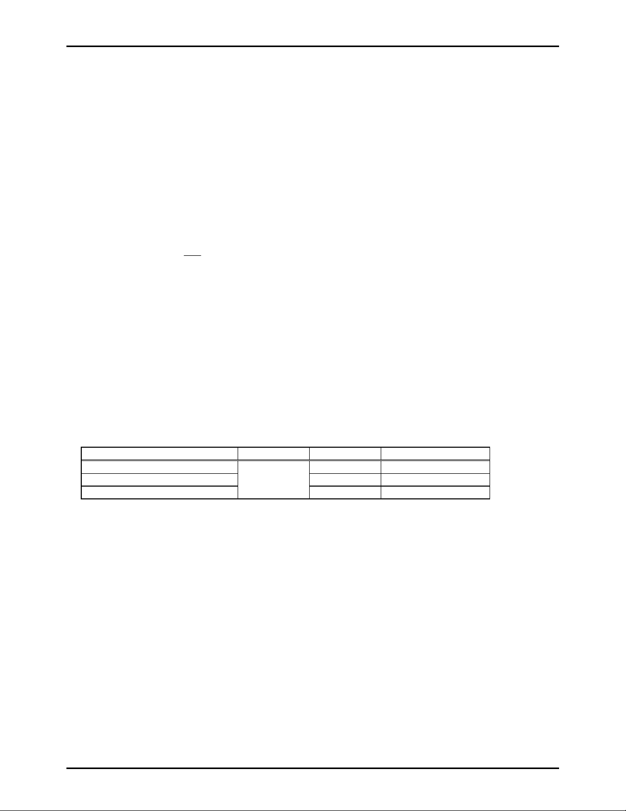
(3) Bus Cycle Time / Instruction Cycle Time
The bus cycle time indicates the speed to read ROM.
Bus cycle time Cycle time Cl ock divider System clock oscillation Oscillation Frequency Voltage
0.5µs 1µs 1/1 Ceramic resonator oscillation 6MHz 4.5 - 6.0V
2µs 4µs 1/2 Ceramic resonator oscillation 3MHz 4.5 - 6.0V
7.5µs 15µs 1/2 RC resonator oscillation 800MHz 4.5 - 6.0V
183µs 366µs 1/2 Crystal oscillation 32.768kHZ 4.5 - 6.0V
Note : External resisters (Rf, Rd) are required when X’ tal oscillation is used.
(4) Ports
- Input/output ports : 3 ports (16 terminals : port 1, 7, 8)
Input/output port programmable in a bit
- 15V withstand Input/output ports : 2 ports (16 terminals)
Input/output port programmable nibble unit : 1 port (8 terminals : port 0)
(When the N-channel open drain output is selected, the data in a bit can be inputted.)
Input/output port programmable in a bit : 1 port (8 terminals : port 3)
- Input port : 2 ports (6 terminals : port 7, 8)
- VFD output port : 52 terminals
Large current output for digit : 16 terminals
Pull-down resistor option available
- Other function
Input/output port : 2 ports (12 terminals : port F, G)
Input port : 3 ports (24 terminals : port C, D, E)
(5) VFD automatic display controller
- Segment/digit output pattern programmable
Any segment/digit combination available
VFD parallel-drive available
- 16-step dimmer function available
(6) AD converter
- 8-channels × 8-bit AD converter
(7) Serial interface
- 1-channel × 16-bit serial interface circuits
- 1-channel × 8-bit serial interface circuits
- LSB first/MSB first function available
- Internal 8-bit baud-rate generator in common with two serial interface circuits
- SIO automatic transmission available (2-32 byte data can be transmitted with program automatically and
continuously.)
No.6700-2/21
Page 3

LC866548/40/32/28/24A
(8) Timers
- Timer 0 : 16-bit timer/counter with 2-bit prescaler + 8-bit programmable prescaler
Mode 0 : Two 8-bit timers with programmable prescaler
Mode 1 : 8-bit timer with a programmable prescaler + 8-bit counter
Mode 2 : 16-bit timer with a programmable prescaler
Mode 3 : 16-bit counter
CYC
The resolution of Timer is t
CYC : cycle time)
. (t
- Timer 1 : 16-bit timer/PWM with
Mode 0 : Two 8-bit timers
Mode 1 : 8-bit timer + 8-bit PWM
Mode 2 : 16-bit timer
Mode 3 : Variable-bit PWM (9-16 bits)
In Mode 0 and Mode 1, the resolution of Timer and PWM is t
In Mode 2 and Mode 3, the resolution of Timer and PWM selectable : t
CYC
.
or 1/2tCYC by prog ram
CYC
- Base timer
Every 500ms overflow system for a clock application (using 32.768kHz crystal oscillation for Base timer
clock)
Every 976
s, 3.9ms, 15.6ms, 62.5ms overflow system (using 32.768kHz crystal oscillation for Base timer
µ
clock)
The Base timer clock selectable ; 32.768kHz crystal oscillation, System clock, and programmable prescaler
output of Timer 0
(9) Buzzer output
- The Buzzer sound frequency selectable ; 4kHz, 2kHz (using 32.768kHz crystal oscillation for Base timer clock)
(10) Remote control receiver circuit (connected to the P73/INT3/T0IN terminal)
- Noise rejection function (the time constant of noise rejection filter : 1tCYC/16tCYC/64tCYC)
(tCYC : instruction cycle time)
- Polarity switching
(11) Watchdog timer
- The watchdog timer is taken on RC outside
- Watchdog timer operation selectable : interrupt system, system reset
(12) Interrupt system
- 14-sourc e 10-vectored inte rrupts :
1. External Interrupt INT0 (include watchdog timer)
2. External Interrupt INT1
3. External Interrupt INT2, Timer/counter T0L (Lower 8 bits)
4. External Interrupt INT3, base timer
5. Timer/counter T 0H (Upper 8 bits)
6. Timer T 1H / T1L
7. Serial interface SIO0
8. Serial interface SIO1
9. AD converter
10. VFD automatic display controller, Port 0
- Built-in Interrupt priority control register
Microcontroller allows 3 levels of interrupt ; low level, high level, and highest level of multiplex interrupt. It can
specify a low level or a high level interrupt priority from INT2/T0L through port 0 (i. e. the above interrupt
number fro m three thro ugh ten). I t can also spe cify a low leve l or the high est level in terrup t priori ty to INT 0 and
INT1.
(13) Subroutine stack levels
- 128 levels (Max.) : Stack area included in RAM area
No.6700-3/21
Page 4
LC866548/40/32/28/24A
(14) Multiplication and division
- 16 bit × 8 bit (7 instruction cycle times)
- 16 bit ÷ 8 bit (7 instruction cycle times)
(15) Three oscillation circuits
- On-chip RC oscillation circuit used for the system clock
- On-chip CF oscillation circuit used for the system clock
- On-chip Crystal oscillation circuit used for the system clock and for time-base clock
Note : External resisters (Rf, Rd) are required
(16) Standby function
- HALT mode function
The HALT mode is used to reduce the power dissipation. In this operation mode, the program execution is stopped.
This operation mode can be released by the interrupt request signals or the initial system reset request signal.
- HOLD mode function
The HOLD mode is used to stop all the oscillations ;
RC (internal), CF and Crystal oscillations. This mode can be released by the following operations.
• Reset terminal (
RES
) set to low level.
• Input a assigned level to P70/INT0/T0I N or P 71/INT1/T0IN terminal.
• Input a Port0 interrupt condition.
(17) Factory shipment
QFP100E delivery form
(18) Development Tools
- Evaluation chip : LC866094
- EPROM version : LC86E6548
- One time version : LC86P6548
- Emulator : EVA86000 + ECB866500 (Evaluation chip board) + POD866500 (P od)
• Notes for use
Follow the unde r table.
Frequency range of the system clock Voltage range Clock Divider Note
15kHz to 3MHz 1/1 Can no t use 1/2 divider
30kHz to 6MHz 1/1, 1/2
Internal RC oscillation
4.5V to 6.0V
1/1, 1/2
No.6700-4/21
Page 5

Pin Assignment QIP100E
Z
N
N
S47/PF7
S46/PF6
S45/PF5
S48/PG0
S49/PG1
S50/PG2
S51/PG3
P00
P01
P02
P03
VSS2
VDD2
P04
P05
P06
P07
P10/SO0
P11/SI0/SB0
P12/SCK0
P13/SO1
P14/SI1/SB1
P15/SCK1
8079787776757473727170696867666564636261605958575655545352
81
82
83
84
85
86
87
88
89
90
91
92
93
94
95
96
97
98
99
100
1 2 3 4 5 6 7 8 9
P30
P16/BUZ
P17/PWM0
Package Dimension
(unit : mm)
3151
LC866548/40/32/28/24A
S44/PF4
S43/PF3
S42/PF2
S41/PF1
S40/PF0
VDD4
S39/PE7
S38/PE6
S37/PE5
S36/PE4
S35/PE3
S34/PE2
S33/PE1
S32/PE0
S31/PD7
S30/PD6
S29/PD5
S28/PD4
S27/PD3
S26/PD2
S25/PD1
S24/PD0
S23/PC7
S22/PC6
S21/PC5
S20/PC4
VP
51
50
S19/PC3
49
S18/PC2
48
S17/PC1
47
S16/PC0
46
VDD3
45
S15/T15
44
S14/T14
43
S13/T13
42
S12/T12
41
S11/T11
40
S10/T10
39
S9/T9
38
S8/T8
37
S7/T7
36
S6/T6
35
S5/T5
34
S4/T4
33
S3/T3
32
S2/T2
31
S1/T1
10
11
12
13
14
15
16
17
18
19
20
21
22
23
24
25
26
27
28
29
30
P31
P32
P33
P34
P35
P36
P37
RES
P70/INT0
CF1
CF2
VSS1
XT1/P74
XT2/P75
VDD1
P80/AN0
P81/AN1
P82/AN2
P83/AN3
P84/AN4
P85/AN5
P86/AN6
P87/AN7
S0/T0
P71/INT1
P72/INT2/T0I
P72/INT3/T0I
SANYO : QIP-100E
No.6700-5/21
Page 6

System Block Diagra m
LC866548/40/32/28/24A
Interrupt Control
IR
PLA
Base Timer
SIO0
SIO1
Timer 0
Standby Contr ol
CF
RC
X’tal
Clock
Generator
Bus Interface ACC
Port 1
Port 3
Port 7
ROM
PC
B Register
C Register
ALU
Timer 1
ADC
INT0 to 3
Noise Filtter
SI0 Automatic
transmission
RAM
128 bytes
VFD Controller
High Voltage Output
Port 8
PSW
RAR
RAM
Stack Pointer
Port 0
Watch dog Timer
No.6700-6/21
Page 7

LC866548/40/32/28/24A
LC866548A/40A/32A/28A/24A Pin Description
Pin Name I/O Function Description Option
VSS1, 2 Power pin (-) *1
VDD1,2,3,4 Power pin (+) *1
VP Power pin (+) for the VFD output pull-down resist
Port 0
P00 - P07
Port 1 •8-bit Input/output port
P10 - P17
Port 3
P30 - P37
Port 7 •4-bit input/output port
P70 - P73
P74
- P75
Port 8
P80 - P83
P84 - P87
S0/T0 to
S6/T6
I/O •8-bit input/output port
Input/output in nibble units
•Input for port 0 interrupt
•Input for HOLD release
•15V withstand at N-channel open drain output
I/O
Input/output can be specified in bit unit.
•Other pin functions
P10
I/O •8-bit input/output port
Input/output in bit unit
•15V withstand at N-channel open drain output
I/O
Input/output in bit unit
I
•2-bit input port
•Other pin function
P70
•Interrupt recei ved form, vector address
rising falling rising/
INT0
INT1
INT2
INT3
•4-bit input/output port
I
Input/output in bit unit
I/O
•4-bit input port
•Other function
AD input port (8 port pins)
O Output for VF D display controller
segment/timing in common
SIO0 data output
P11
SIO0 data input/bus input/output
P12
SIO0 clock input/output
P13
SIO1 data output
P14
SIO1 data input/bus input/output
P15
SIO1 clock input/output
P16
Buzzer output
P17
Timer1 output (PWM0 output)
INT0 input/HOLD release /Nch-Tr.
output for watchdog timer
P71
INT1 input/HOLD release input
P72
INT2 input/timer 0 event input
P73
INT3 input with noise filter/timer 0
event input
P74
Input pin XT1 for 32.768kHz crystal
resonator oscillation
P75
Output pin XT2 for 32.768kHz
crystal resonator oscillation
enable
enable
enable
enable
enable
enable
enable
enable
falling
disable
disable
enable
enable
H level L level Vector
enable
enable
disable
disable
•Pull-up resistor :
Provided/Not provided (each nibble)
•Output form :
CMOS/N-channel open drain
(each bit)
•Output form :
CMOS/N-channel open drain
(each bit)
•Output form :
CMOS/N-channel open drain
(each bit)
enable
enable
disable
disable
Pull-down resistor :
Provided/Not provided (each bit)
03H
0BH
13H
1BH
(continue)
No.6700-7/21
Page 8

LC866548/40/32/28/24A
Pin Name I/O Function Description Option
S7/T7 to
S15/T15
S16 to S31 I/O
S32 to S47 I/O
S48 to S51 I/O
I Reset pin
RES
P74
XT1/
O •Output for VFD display controller
segment/timing with internal pull-down
resistor in common
•Internal pull-down resistor output
•Output for VFD display controller segment
•Other function
S16 : High voltage input port PC0
S17 : High voltage input port PC1
S18 : High voltage input port PC2
S19 : High voltage input port PC3
S20 : High voltage input port PC4
S21 : High voltage input port PC5
S22 : High voltage input port PC6
S23 : High voltage input port PC7
S24 : High voltage input port PD0
S25 : High voltage input port PD1
S26 : High voltage input port PD2
S27 : High voltage input port PD3
S28 : High voltage input port PD4
S29 : High voltage input port PD5
S30 : High voltage input port PD6
S31 : High voltage input port PD7
•Output for VFD display controller segment
•Other function
S32 : High voltage input port PE0
S33 : High voltage input port PE1
S34 : High voltage input port PE2
S35 : High voltage input port PE3
S36 : High voltage input port PE4
S37 : High voltage input port PE5
S38 : High voltage input port PE6
S39 : High voltage input port PE7
S40 : High voltage I/O port PF0
S41 : High voltage I/O port PF1
S42 : High voltage I/O port PF2
S43 : High voltage I/O port PF3
S44 : High voltage I/O port PF4
S45 : High voltage I/O port PF5
S46 : High voltage I/O port PF6
S47 : High voltage I/O port PF7
•Output for VFD display controller segment
•Other function
S48 : High voltage I/O port PG0
S49 : High voltage I/O port PG1
S50 : High voltage I/O port PG2
S51 : High voltage I/O port PG3
I •Input pin for 32.768kHz crystal oscillation
•Other function
P74
for input port
In case of non use, connect to VDD1.
Pull-down resistor :
Provided/Not provided (each bit)
Pull-down resistor :
Provided/Not provided (each bit)
(continue)
No.6700-8/21
Page 9

LC866548/40/32/28/24A
Pin Name I/O Function Description Option
XT2/P75 O •Output pin for 32.768kHz crystal oscillation
•Other function
P75 for input port
•In case of non use,
At using as oscillator, should be left opened.
At using as a port, connect to VDD1.
CF1 I Input pin for ceramic resonator oscillation
CF2 O Output pin for ceramic resonator oscillation
* All of port options (except pull-up resistor of port 0) can be specified in bit unit.
* A state of pins at reset
Pin name Input/output mode A state of pull-up resistor specified at pull-up option
Port 0 Input Fixed pull-up resistor OFF
Ports 1, 3 Input Programmable pull-up resistor OFF
S0/T0 to S15/T15 P channel Transistor OFF
S16 to S51 P channel Transistor OFF
*1 Connect like the following figure to reduce noise into a VDD1 terminal.
• Shorted the VSS1 terminal to the VSS2 terminal and to make the back-up time long.
Power
Supply
Back-up capacitor
LSI
VDD1
VDD2
VDD3
VFD
powers
VDD4
VSS2 VSS1
No.6700-9/21
Page 10

LC866548/40/32/28/24A
1. Absolute Maximum Ratings at VSS1=VSS2=0V and Ta=25°C
Parameter Symbol Pins Conditions
Supply voltage VDD MAX VDD1, VDD2
VDD3, VDD4
Input voltage
VI(1)
•Ports
74
,75
VDD1=VDD2
=VDD3=VDD4
-0.3
•Ports 80,81,82,
83
•Port 8
RES
•
VI(2) VP
Output voltage VO S0/T0-S15/T15
Input/output
voltage
VIO(1) •Port 1
•Ports 70,71,72,
-0.3
73
•Ports 84,85,86,
87
•Ports 0, 3 at
CMOS output
option
VIO(2) Ports 0, 3 at
-0.3 15
N-ch open drain
output option
VIO(3) S16 - S51
High
level
output
current
Low
level
output
current
Peak
output
current
Total
output
current
output
current
IOPH(1) Ports 0, 1, 3 •CMOS output
•For each pin.
IOPH(2) S0/T0-S15/ T1 5 For each pin. -30
IOPH(3) S16 - S51 For each pin. -15
IOAH(1) Port 0 -30
Σ
IOAH(2) Ports 1, 3 -30
Σ
IOAH(3) S0/T0-S15/T15 -55
Σ
IOAH(4) S16 - S27 -60
Σ
IOAH(5) S28 - S39 -60
Σ
IOAH(6) S40 - S51
Σ
IOPL(1) Ports 0, 1, 3 20 Peak
The total of all
pins.
For each pin.
IOPL(2) •Ports 70,71,72,
73
•Ports 84,85,86,
87
Total
output
current
IOAL(1) Port 0 60
Σ
IOAL(2) Ports 1, 3, 70 50
Σ
IOAL(3) •Ports 71,72, 73
Σ
The total of all
pins.
•Ports 84,85,86,
87
Power dissipation
Pdmax QFP100E Ta=-30 to+70°C 500 mW
(max.)
Operating
Topr -30 70
temperature
range
Storage
Tstg -55 125
temperature
range
Ratings
VDD[V] min. typ. max.
-0.3 +7.0
VDD+0.3
VDD-45
VDD-45
VDD-45
VDD+0.3
VDD+0.3
VDD+0.3
VDD+0.3
-10
-60
15
20
unit
V
mA
C
°
No.6700-10/21
Page 11

LC866548/40/32/28/24A
2. Recommended Operating Range at Ta=-30°C to +70°C, VSS1=VSS2=0V
Parameter Symbol Pins Conditions
Operating
supply voltage
VDD(1) VDD1=VDD2
=VDD3=VDD4
0.98µs ≤ tCYC
tCYC ≤ 400µs
range
Hold voltage VHD VDD1=VDD2 RAMs and the
Registers hold voltage
at HOLD mode.
Pull-down
VP VP 4.5 - 6.0 -35 VDD
voltage
Input high
voltage
VIH(1) Port 0 at CMOS
output option
VIH(2) Port 0 at N-ch
Output disable 4.5 - 6.0
Output disable 4.5 - 6.0
open drain output
VIH(3) •Port 1
Output disable 4.5 - 6.0
•Ports 72, 73
•Port 3 at CMOS
output option
VIH(4) Port 3 at N-ch
open drain output
VIH(5) •Port 70
Output disable Tr.
OFF
Output disable 4.5 - 6.0
port input
/interrupt
•Port 71
•
RES
VIH(6) Port 70
Output disable 4.5 - 6.0 0.9VDD VDD
Watchdog timer
VIH(7) •Port 8
74
•Ports
, 75
Output disable 4.5 - 6.0
VIH(8) S16 - S51 Output P-channel Tr.
OFF
Input low
voltage
VIL(1) Port 0 at CMOS
output option
VIL(2) Port 0 at N-ch
Output disable 4.5 - 6.0 VSS 0.2VDD
Output disable 4.5 - 6.0 VSS
open drain output
VIL(3) •Ports 1, 3
Output disable 4.5 - 6.0 VSS
•Ports 72, 73
VIL(4) •Port 70
Output disable 4.5 - 6.0 VSS
port input
/interrupt
•Port 71
RES
•
VIL(5) Port 70
Output disable 4.5 - 6.0 VSS 0.8VDD
Watchdog timer
VIL(6) •Port 8
74
, 75
•Ports
Output disable 4.5 - 6.0 VSS
VIL(7) S16 - S51 Output P-channel Tr.
OFF
Operation
tCYC 4.5 - 6.0 0.98 400
cycle time
Ratings
VDD[V] min. typ. max.
4.5 6.0
2.0 6.0
0.33VDD
+1.0
0.75VDD
0.75VDD
4.5 - 6.0
0.75VDD
0.75VDD
0.75VDD
4.5 - 6.0
0.33VDD
+1.0
4.5 - 6.0 VP 0.2VDD
(continue)
unit
VDD
13.5
VDD
13.5
VDD
VDD
VDD
0.25VDD
0.25VDD
0.25VDD
-1.0
0.25VDD
µ
V
s
No.6700-11/21
Page 12

LC866548/40/32/28/24A
Parameter Symbol Pins Conditions
Oscillation
frequency
range
(Note 1)
Oscillation
stable time
period
(Note 1)
FmCF(1) CF1, CF2 •6MHz (ceramic
resonator oscillation)
•Refer to figure 1
FmCF(2) CF1, CF2 •3MHz (ceramic
resonator oscillation)
•Refer to figure 1
FmRC RC oscillation 4.5 - 6.0 0.3 0.8 3.0
FsX’tal XT 1, XT2 •32.768kHz (crystal
oscillation)
•Refer to figure 2
tmsCF(1) CF1, CF2 •6MHz (ceramic
resonator oscillation)
•Refer to figure 3
tmsCF(2) CF1, CF2 •3MHz (ceramic
resonator oscillation)
•Refer to figure 3
tssX’tal XT1, XT2 •32.768kHz (cry stal
oscillation)
•Refer to figure 3
(Note 1) The oscillation constant is shown on table 1.
Ratings
VDD[V] min. typ. max.
4.5 - 6.0 6
4.5 - 6.0 3
4.5 - 6.0 32.768 kHz
4.5 - 6.0 0.1 3.0
4.5 - 6.0 0.1 3.0
4.5 - 6.0 0.7 1.0 s
unit
MHz
ms
No.6700-12/21
Page 13

LC866548/40/32/28/24A
3. Electrical Characteristics at Ta=- 30°C to +70°C, VSS1=VSS2=0V
Parameter Symbol Pins Conditions
Input high
current
Input low
current
Output high
voltage
IIH(1) Ports 0, 3 of open
drain output
IIH(2) •Port 0 without
pull-up MOS Tr.
•Ports 1, 3
IIH(3) •Ports70,71,72,73
•Port 8
IIH(4)
IIH(5) Ports74, 75 VIN=VDD 4.5 - 6.0 1
IIH(6) S16 to S51
IIL(1) •Ports 1, 3
IIL(2) •Ports70,71,72,73
IIL(3)
IIL(4) Ports
VOH(1) IOH=-1.0mA 4.5 - 6.0 VDD-1
VOH(2)
VOH(3) IOH=-20mA 4.5 - 6.0
VOH(4)
VOH(5) IOH=-5mA 4.5 - 6.0
VOH(6)
RES
VIN=VDD 4.5 - 6.0 1
without pull-down
resistor (Ports C,
D, E, F,G)
•Port 0 without
pull-up MOS Tr.
•Port 8
RES
VIN=VSS 4.5 - 6.0 -1
, 75 VIN=VSS 4.5 - 6.0 -1
74
Ports 0, 1, 3 of
CMOS output
S0/T0 to S15/T15
S16 to S51
•Output disable
•VIN=13.5V
(including off-leak
current of the
output Tr.)
•Output disable
•Pull-up MOS Tr.
OFF
•VIN=VDD
(including off-leak
current of the
output Tr.)
•Output disable
•VIN=VDD
(including off-leak
current of the
output Tr.)
•Output P-channel
Tr. OFF
•VIN=VDD
•Output disable
•Pull-up MOS Tr.
OFF
•VIN=VSS
(including off-leak
current of the
output Tr.)
•Output disable
•VIN=VSS
(including off-leak
current of the
output Tr.)
IOH=-0.1mA 4.5 - 6.0
•IOH=-1mA
•The current of any
unmeasurement pin
is not over 1mA.
The current of any
unmeasurement pin
is not over 1mA.
VDD[V] min. typ. max.
4.5 - 6.0 5
4.5 - 6.0 1
4.5 - 6.0 1
4.5 - 6.0 1
4.5 - 6.0 -1
4.5 - 6.0 -1
4.5 - 6.0 VDD-1
4.5 - 6.0 VDD-1
Ratings
VDD-0.5
VDD-1.8
VDD-1.8
unit
µ
µ
V
A
A
(continue)
No.6700-13/21
Page 14

LC866548/40/32/28/24A
Parameter Symbol Pins Conditions
Output low
voltage
Pull-up MOS
Tr. resistor
leak current
Resistance of
the low level
hold Tr.
High voltage
pull-down
resistor
VP pull-down
resistor
Hysteresis
voltage
Pin
capacitance
VOL(1) IOL=10mA 4.5 - 6.0 1.5
VOL(2)
VOL(3) Port 70 IOL=1mA 4.5 - 6.0 0.4
VOL(4) •Ports 71, 72, 73
Rpu Ports 0, 1, 3 VOH=0.9VDD 4.5 - 6.0 15 40 70 KΩ
IOFF(1) •Output P-ch Tr.
IOFF(2)
Rinpd S16 to S51 •Output P-ch Tr.
Rpd S0/T0 to S15/T15,
Rvppd Vp •VSS=GND
VHIS •Port 1
CP All pins •f=1MHz
Ports 0, 1, 3
•Ports84,85,86,87
S0/T0 to S6/T6,
S16 to S51 without pull-down
resistor
S16 to S51 with
pull-down resistor
•Ports 70, 71, 72,
73, 75
•
RES
IOL=1.6mA 4.5 - 6.0 0.4
IOL=1.6mA 4.5 - 6.0 0.4
OFF
•VOUT=VSS
•Output P-ch Tr.
OFF
•VOUT=VDD-40V
OFF
•Using as input
ports
•Output P-ch Tr.
OFF
•VOUT=3V
•Vp=-30V
•Vp=-30V
Output disable 4.5 - 6.0 0.1
•Unmeasurement
terminals for the
input are set to
VSS level.
•Ta=25°C
Ratings
VDD[V] min. typ. max.
4.5 - 6.0 -1 Output off-
4.5 - 6.0 -30
4.5 - 6.0 200
5.0 60 100 200
5.0 60 100 200
VDD
4.5 - 6.0 10 pF
unit
V
A
µ
kΩ
V
No.6700-14/21
Page 15

LC866548/40/32/28/24A
4. Serial Input/Output Characteristics at Ta=-30°C to +70°C, VSS1=VSS2=0V
Parameter Symbol Pins Conditions
Cycle
Low Level
pulse width
Input clock
High Level
pulse width
Cycle
Serial clock
Low Level
pulse width
High Level
Output clock
pulse width
Data set up ti me
Data hold time
Serial input
Output delay
time
(Serial clock is
external clock)
Output delay
time
Serial output
(Serial clock is
internal clock)
tCKCY(1) 2
tCKL(1) 1
tCKH(1)
tCKCY(2) 2
tCKL(2)
tCKH(2)
tICK 0.1
tCKI
tCKO(1)
tCKO(2)
•SCK0
•SCK1
•SCK0
•SCK1
SI0 SI1
SB0 SB1
SO0 SO1
SB0 SB1
Refer to figure 5. 4.5 - 6.0
•Use pull- up
resistor (1kΩ)
when open drain
output.
•Refer to figure 5.
•Data set-up to
SCK0, 1.
•Data hold from
SCK0, 1.
•Refer to figure 5.
•Use pull- up
resistor (1kΩ)
when open drain
output.
•Data hold from
SCK0, 1
•Refer to figure 5.
Ratings
VDD[V] min. typ. max.
1
4.5 - 6.0
4.5 - 6.0
0.1
4.5 - 6.0
5. Pulse Input Conditions at Ta=-30°C to +70°C, VSS1=VSS2=0V
Parameter Symbol Pins Conditions
High/low level
pulse width
tPIH(1)
tPIL(1)
tPIH(2)
tPIL(2)
tPIH(3)
tPIL(3)
tPIH(4)
tPIL(4)
tPIL(5)
•INT0, INT1
•INT2/T0IN
INT3/T0IN
(The noise
rejection clock is
select to 1/1.)
INT3/T0IN
(The noise
rejection clock is
select to 1/16.)
INT3/T0IN
(The noise
rejection clock is
select to 1/64.)
Reset acceptable 4.5 - 6.0 200
RES
•Interrupt acceptable
•Timer0-countable
•Interrupt accept able
•Timer0-countable
•Interrupt accept able
•Timer0-countable
•Interrupt accept able
•Timer0-countable
Ratings
VDD[V] min. typ. max.
4.5 - 6.0 1
4.5 - 6.0 2
4.5 - 6.0 32
4.5 - 6.0 128
1/2tCKCY
1/2tCKCY
7/12tCYC
+0.2
1/3tCYC
+0.2
unit
tCYC
s
µ
unit
tCYC
s
µ
No.6700-15/21
Page 16

LC866548/40/32/28/24A
6. AD Converter Characteristics at Ta=-30°C to + 70°C, VSS1=VSS2=0V
Parameter Symbol Pins Conditions
Resolution N 4.5 - 6.0 8 bit
Absolute
precision
(Note2)
Conversion
time
Analog input
voltage range
input current
ET 4.5 - 6.0 ±1.5 LSB
tCAD
VAIN 4.5 - 6.0 VSS VDD V
IAINH VAIN=VDD 4.5 - 6.0 1 Analog port
IAINL
AN0 - AN7
AD conversion time
tCYC
=16
×
(ADCR2=0) *Note3
AD conversion time
tCYC
=32
×
(ADCR2=1) *Note3
VAIN=VSS 4.5 - 6.0 -1
Ratings
VDD[V] min. typ. max.
4.5 - 6.0 15.68
(tCYC
=0.98µs)
4.5 - 6.0 31.36
(tCYC
=0.98µs)
65.28
(tCYC
=4.08µs)
130.56
(tCYC
=4.08µs)
unit
s
µ
A
µ
(Note 2) Absolute precision excepts quantizing error (±1/2 LSB).
(Note 3) The conversion time means the time from executing the AD conversion instruction to setting the complete digital
conversion value to the register.
7. Current Dissipation Characteristics at Ta=-30°C to +70°C, VSS1=VSS2=0V
Parameter Symbol Pins Conditions
Current
dissipation
during basic
operation
(Note 4)
IDDOP(1) •FmCF=6MHz
IDDOP(2) •FmCF=3MHz
IDDOP(3) •FmCF=0Hz
IDDOP(4)
Ceramic resonator oscillation
•Internal RC oscillation stops.
•FsXtal=32.768kHz
Crystal oscillation
•System clock : CF oscillation
•1/1 divided
Ceramic resonator oscillation
•Internal RC oscillation stops.
•FsXtal=32.768kHz
Crystal oscillation
•System clock : CF oscillation
•1/2 divided
(when oscillation stops)
•FsXtal=32.768kHz
Crystal oscillation
•System clock : RC oscillation
•1/2 divided
•FmCF=0Hz
(when oscillation stops)
•FsXtal=32.768kHz
Crystal oscillation
•System clock :
Crystal oscillation
•Internal RC oscillation stops.
•1/2 divided
Ratings
VDD[V] min. typ. max.
4.5 - 6.0 10 25
4.5 - 6.0 3 9
4.5 - 6.0 0.7 3.4
4.5 - 6.0 35 130 µA
unit
mA
No.6700-16/21
Page 17

LC866548/40/32/28/24A
Parameter Symbol Pins Conditions
Current
dissipation
HALT mode
(Note 4)
Current
dissipation
HOLD
mode
(Note 4)
IDDHALT(1) •HALT mode
•FmCF=6MHz
Ceramic resonator oscillation
•FsXtal=32.768kHz
Crystal oscillation
•Internal RC oscillation stops.
•System clock : CF oscillation
•1/1 divided
IDDHALT(2) •HALT mode
•FmCF=3MHz
Ceramic resonator oscillation
•FsXtal=32.768kHz
Crystal oscillation
•Internal RC oscillation stops.
•System clock : CF oscillation
•1/2 divided
IDDHALT(3) •HALT mode
•FmCF=0Hz
(when oscillation stops)
•FsXtal=32.768kHz
Crystal oscillation
•System clock : RC oscilaltion
•1/2 divided
IDDHALT(4) •HALT mode
•FmCF=0Hz
(when oscillation stops)
•FsXtal=32.768kHz
Crystal oscillation
•System clock :
Crystal oscilaltion
•Internal RC oscillation stops.
•1/2 divided
IDDHOLD(1) HOLD mode
Ratings
VDD[V] min. typ. max.
4.5 - 6.0 5 14
4.5 - 6.0 2.2 7
4.5 - 6.0 400 1600
4.5 - 6.0 25 100
4.5 - 6.0 0.05 30
(Note 4) The currents of the output transistors and the pull-up MOS transistors are ignored.
Table 1. Ceramic resonator oscillation guaranteed constant (main clock)
Oscillation type Maker Oscillator C1 C2
6MHz ceramic resonator
oscillation
Kyocera
3MHz ceramic resonator
oscillation
Kyocera KBR-3.0MS 33pF 33pF
CSA6.00MG 33pF 33pF Murata
CST6.00MGW on chip
KBR-6.0MSB 33pF 33pF
PBRC6.00A (chip type) 33pF 33pF
KBR-6.0MKC
PBRC6.00B (chip type)
CSA3.00MG 33pF 33pF Murata
CST3.00MGW on chip
on chip
* Both C1 and C2 must be a K rank (±10%) and SL characteristics.
unit
mA
A
µ
A
µ
No.6700-17/21
Page 18

LC866548/40/32/28/24A
Table 2. Crystal oscillation guaranteed constant (sub clock)
Oscillation type Maker Oscillator C1 C2 Rf Rd
32.768kHz crystal
oscillation
EPSON C-002RX 18pF 18pF 10MΩ 680kΩ
CITIZEN
CFS-308
CFS-206
18pF 18pF 10MΩ 330kΩ
* Both C3 and C4 must use J rank (±5%) and CH characteristics.
(It is about the application which is not in need of high precision. Use K rank (±10%) and SL characteristics.)
(Notes) •Since the circuit pattern affects the oscillation frequency, place the oscillation-related parts as close to the oscillation
pins as possible with the shortest possible pattern length.
•If you use other oscillators herein, we provide no guarantee for the characteristics.
CF2 CF1
XT2 XT1
Rf
X’tal
Rd
C4
C1
CF
C2
C3
Figure 1 Ceramic oscillation circuit Figure 2 Crystal oscillation circuit
No.6700-18/21
Page 19

LC866548/40/32/28/24A
r
f
y
Power suppl
RES
Reset time
Internal RC
resonator oscillation
tmsCF
CF1, CF2
tssXtal
XT1, XT2
Operation mode
Unfixed Reset Instruction execution mode
Instruction
execution mode
OCR6=1
< Reset time and oscillation stabilizing time. >
HOLD release signal
Valid
Internal RC
resonator oscillation
tmsCF
CF1, CF2
tssXtal
XT1, XT2
Operation mode
HOLD Instruction executio n mode
< HOLD release signal and oscillation stabilizing time. >
Figure 3 Oscillation stable time
VDD
RES
R
RES
(Note) Fix the value of C
sure to reset until 200µs, after Powe
supply has been over inferior limit o
RES
C
supply voltage.
Figure 4 Reset circuit
VDD
VDD limit
0V
RES
, R
RES
that is
No.6700-19/21
Page 20

LC866548/40/32/28/24A
,
<AC timing point>
0.5VDD
tCKCY
VDD
tCKL tCKH
SCK0
SCK1
SI0
SI1
tCKO
SO0, SO1
SB0
SB1
tICK tCKI
<Timing>
1kΩ
50pF
<Test load>
Figure 5 Serial input / output test condition
tPIL tPIH
Figure 6 Pulse input timing condition
No.6700-20/21
Page 21

LC866548/40/32/28/24A
No.6700-21/21
PS
 Loading...